REV. A
Information furnished by Analog Devices is believed to be accurate and
reliable. However, no responsibility is assumed by Analog Devices for its
use, nor for any infringements of patents or other rights of third parties
which may result from its use. No license is granted by implication or
otherwise under any patent or patent rights of Analog Devices.
a
AD8310
One Technology Way, P.O. Box 9106, Norwood, MA 02062-9106, U.S.A.
Tel: 781/329-4700
World Wide Web Site: http://www.analog.com
Fax: 781/326-8703
© Analog Devices, Inc., 1999
Fast, Voltage-Out DC-440 MHz
95 dB Logarithmic Amplifier
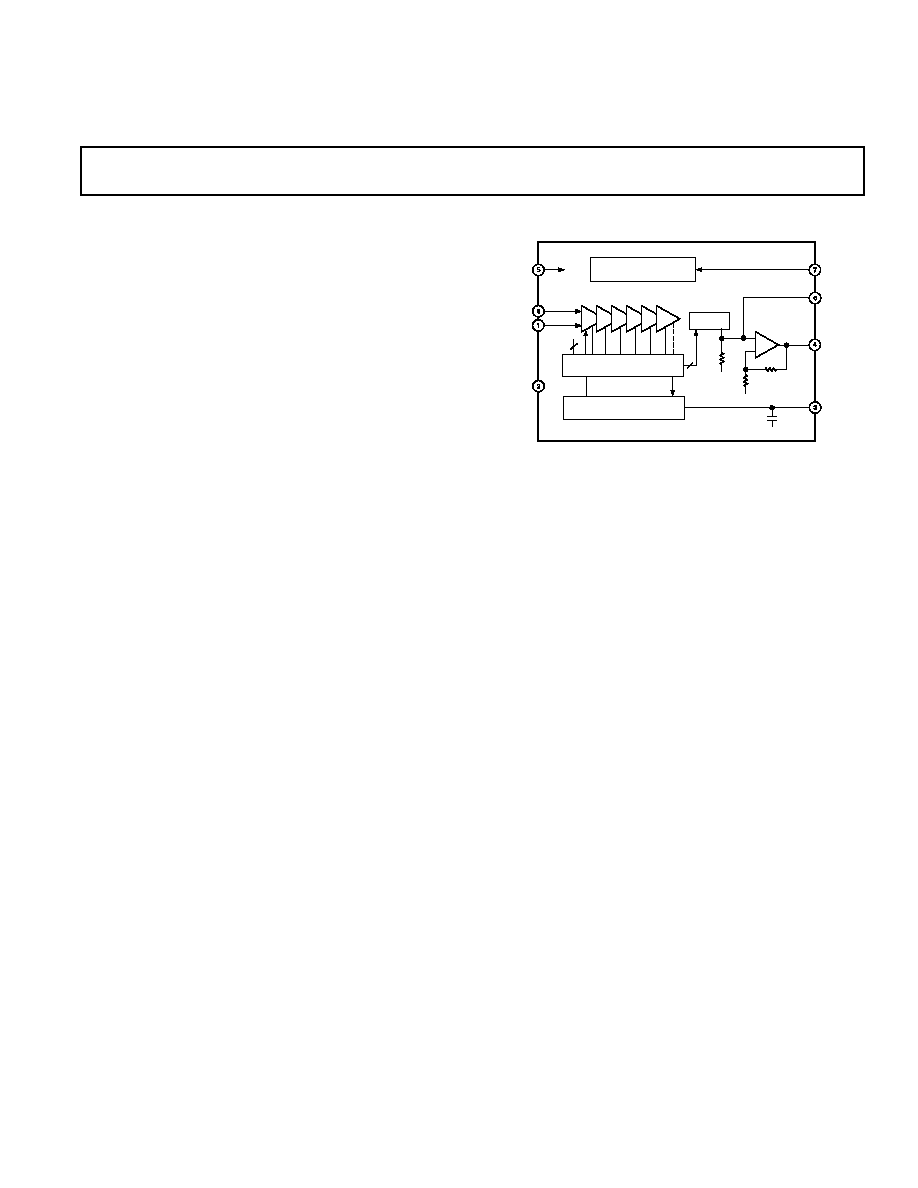
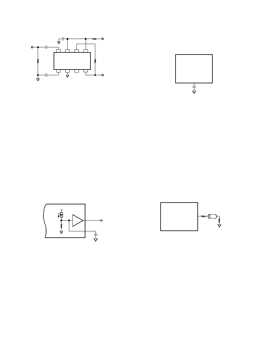
FUNCTIONAL BLOCK DIAGRAM
+
≠
VPOS
INHI
INLO
COMM
3
8mA
1.0k
BANDGAP REFERENCE
AND BIASING
SIX 14.3dB 900MHz
AMPLIFIER STAGES
NINE DETECTOR CELLS
SPACED 14.3dB
INPUT-OFFSET
COMPENSATION LOOP
2
2 A
/dB
MIRROR
3k
3k
1k
COMM
COMM
COMM
ENBL
BFIN
VOUT
OFLT
ENABLE
BUFFER
INPUT
OUTPUT
OFFSET
FILTER
AD8310
SUPPLY
+INPUT
≠INPUT
COMMON
33pF
FEATURES
Multistage Demodulating Logarithmic Amplifier
Voltage Output, Rise-Time <15 ns
High-Current Capacity: 25 mA into Grounded R
L
95 dB Dynamic Range: ≠91 dBV to +4 dBV
Single Supply of 2.7 V Min at 8 mA Typ
DC-440 MHz Operation, 0.4 dB Linearity
Slope of 24 mV/dB, Intercept of ≠108 dBV
Highly Stable Scaling over Temperature
Fully Differential DC-Coupled Signal Path
100 ns Power-Up Time, 1 A Sleep Current
APPLICATIONS
Conversion of Signal Level to Decibel Form
Transmitter Antenna Power Measurement
Receiver Signal Strength Indication (RSSI)
Low-Cost Radar and Sonar Signal-Processing
Network and Spectrum Analyzers
Signal-Level Determination Down to 20 Hz
True-Decibel AC Mode for Multimeters
PRODUCT DESCRIPTION
The AD8310 is a complete, dc-440 MHz demodulating
logarithmic amplifier (log amp) with a very fast voltage-mode
output capable of driving up to 25 mA into a grounded load in
under 15 ns. It uses the progressive compression (successive
detection) technique to provide a dynamic range of up to 95 dB
to
±
3 dB law-conformance, or 90 dB to a
±
1 dB error bound up
to 100 MHz. It is extremely stable and easy to use, requiring no
significant external components. A single supply voltage of 2.7 V
to 5.5 V at 8 mA is needed, corresponding to a power consump-
tion of only 24 mW at 3 V. A fast-acting CMOS-compatible
enable pin is provided.
Each of the six cascaded amplifier/limiter cells has a small-signal
gain of 14.3 dB, with a ≠3 dB bandwidth of 900 MHz. A total
of nine detector cells are used, to provide a dynamic range that
extends from ≠91 dBV (where 0 dBV is defined as the ampli-
tude of a 1 V rms sine wave) that is, an amplitude of about
±
40
µ
V, up to +4 dBV (or
±
2.2 V). The demodulated output
is accurately scaled, with a log slope of 24 mV/dB and an intercept
of ≠108 dBV; the scaling parameters are supply- and temperature-
independent. The fully-differential input offers a moderately
high impedance (1 k
in parallel with about 1 pF). A simple
network can match the input to 50
and provide a power
sensitivity of to ≠78 dBm to +17 dBm. The logarithmic linearity
is typically within
±
0.4 dB up to 100 MHz over the central
portion of the range, but is somewhat greater at 440 MHz. There
is no minimum frequency limit; the AD8310 may be used down
to low audio frequencies. Special filtering features are provided
to support this wide range.
The output voltage runs from a noise-limited lower boundary of
400 mV to an upper limit within 200 mV of the supply voltage
for light loads. The slope and intercept can be readily altered
using external resistors. The output is tolerant of a wide variety
of load conditions and is stable with capacitive loads of 100 pF.
The AD8310 provides a unique combination of low cost, small
size, small power consumption, high accuracy and stability, high
dynamic range, a frequency range encompassing audio to UHF,
fast response time and good load-driving capabilities, making this
product useful in numerous applications requiring the reduction
of a signal to its decibel equivalent.
The AD8310 is available in the industrial temperature range of
≠40
∞
C to +85
∞
C, in an 8-lead Mini_SO package.

≠2≠
REV. A
AD8310≠SPECIFICATIONS
Parameter
Conditions
Min
Typ
Max
Unit
INPUT STAGE
(Inputs INHI, INLO)
Maximum Input
1
Single-Ended, p-p
±
2.0
±
2.2
V
4
dBV
Equivalent Power in 50
Termination Resistor of 52.3
17
dBm
Differential Drive, p-p
20
dBm
Noise Floor
Terminated 50
Source
1.28
nV/
Hz
Equivalent Power in 50
440 MHz Bandwidth
≠78
dBm
Input Resistance
From INHI to INLO
800
1000
1200
Input Capacitance
From INHI to INLO
1.4
pF
DC Bias Voltage
Either Input
3.2
V
LOGARITHMIC AMPLIFIER
(Output VOUT)
±
3 dB Error Dynamic Range
From Noise Floor to Maximum Input
95
dB
Transfer Slope
10 MHz
f
200 MHz
22
24
26
mV/dB
Over Temperature ≠40
∞
C < T
A
< +85
∞
C
20
26
mV/dB
Intercept (Log Offset)
2
10 MHz
f
200 MHz
≠115
≠108
≠99
dBV
Equivalent dBm (re 50
)
≠102
≠95
≠86
dBm
Over Temperature ≠40
∞
C
T
A
+85
∞
C
≠120
≠96
dBV
Equivalent dBm (re 50
)
≠107
≠83
dBm
Temperature Sensitivity
≠0.04
dB/
∞
C
Linearity Error (Ripple)
Input from ≠88 dBV (≠75 dBm) to +2 dBV (+15 dBm)
±
0.4
dB
Output Voltage
Input = ≠91 dBV (≠78 dBm)
0.4
V
Input = 9 dBV (22 dBm)
2.6
V
Minimum Load Resistance, R
L
100
Maximum Sink Current
0.5
mA
Output Resistance
0.05
Video Bandwidth
25
MHz
Rise Time (10%≠90%)
Input Level = ≠43 dBV (≠30 dBm),
R
L
402
, C
L
68 pF
15
ns
Input Level = ≠3 dBV (+10 dBm),
R
L
402
, C
L
68 pF
20
ns
Fall Time (90%≠10%)
Input Level = ≠43 dBV (≠30 dBm),
R
L
402
, C
L
68 pF
30
ns
Input Level = ≠3 dBV (+10 dBm),
R
L
402
, C
L
68 pF
40
ns
Output Settling Time to 1%
Input Level = ≠13 dBV (0 dBm),
R
L
402
, C
L
68 pF
40
ns
POWER INTERFACES
Supply Voltage, V
POS
2.7
5.5
V
Quiescent Current
Zero-Signal
6.5
8.0
9.5
mA
Over Temperature
≠40
∞
C < T
A
< +85
∞
C
5.5
8.5
10
mA
Disable Current
0.05
µ
A
Logic Level to Enable Power
HI Condition, ≠40
∞
C < T
A
< +85
∞
C
2.3
V
Input Current when HI
3 V at ENBL
35
µ
A
Logic Level to Disable Power
LO Condition, ≠40
∞
C < T
A
< +85
∞
C
0.8
V
NOTES
1
The input level is specified in "dBV" since logarithmic amplifiers respond strictly to voltage, not power. 0 dBV corresponds to a sinusoidal single-frequency input of
1 V rms. A power level of 0 dBm (1 mW) in a 50
termination corresponds to an input of 0.2236 V rms. Hence, the relationship between dBV and dBm is a fixed
offset of 13 dBm in the special case of a 50
termination.
2
Guaranteed but not tested; limits are specified at six sigma levels.
Specifications subject to change without notice.
(@ T
A
= 25 C, V
S
= 5 V, unless otherwise noted)
AD8310
≠3≠
REV. A
ABSOLUTE MAXIMUM RATINGS
*
Supply Voltage V
S
. . . . . . . . . . . . . . . . . . . . . . . . . . . . . . 7.5 V
Input Power (re 50
), Single-Ended . . . . . . . . . . . . . 18 dBm
Differential Drive . . . . . . . . . . . . . . . . . . . . . . . . . . . 22 dBm
Internal Power Dissipation . . . . . . . . . . . . . . . . . . . . . 200 mW
JA
. . . . . . . . . . . . . . . . . . . . . . . . . . . . . . . . . . . . . . . 200
∞
C/W
Maximum Junction Temperature . . . . . . . . . . . . . . . . . 125
∞
C
Operating Temperature Range . . . . . . . . . . . . ≠40
∞
C to +85
∞
C
Storage Temperature Range . . . . . . . . . . . . . ≠65
∞
C to +150
∞
C
Lead Temperature Range (Soldering 60 sec) . . . . . . . . . 300
∞
C
*Stresses above those listed under Absolute Maximum Ratings may cause perma-
nent damage to the device. This is a stress rating only; functional operation of the
device at these or any other conditions above those indicated in the operational
section of this specification is not implied. Exposure to absolute maximum rating
conditions for extended periods may effect device reliability.
ORDERING GUIDE
Package
Package
Model
Description
Option
AD8310ARM
*
RM-8 Tube
RM-8
AD8310ARM-REEL
RM-8 13" Tape and Reel
RM-8
AD8310ARM-REEL7
RM-8 7" Tape and Reel
RM-8
AD8310-EVAL
Evaluation Board
*Device branded as J6A.
CAUTION
ESD (electrostatic discharge) sensitive device. Electrostatic charges as high as 4000 V readily
accumulate on the human body and test equipment and can discharge without detection.
Although the AD8310 features proprietary ESD protection circuitry, permanent damage may
occur on devices subjected to high energy electrostatic discharges. Therefore, proper ESD
precautions are recommended to avoid performance degradation or loss of functionality.
WARNING!
ESD SENSITIVE DEVICE
PIN CONFIGURATION
INHI
ENBL
BFIN
VPOS
COMM
OFLT
VOUT
TOP VIEW
(Not to Scale)
8
7
6
5
1
2
3
4
INLO
AD8310
PIN FUNCTION DESCRIPTIONS
Pin
Name
Function
1
INLO
One of two balanced inputs, biased roughly to
VPOS/2.
2
COMM
Common Pin (usually grounded).
3
OFLT
Offset filter access, nominally at about 1.75 V.
4
VOUT
Low impedance output voltage, 25 mA max
load.
5
VPOS
Positive Supply, 2.7 V ≠ 5.5 V at 8 mA quies-
cent current.
6
BFIN
Buffer input; used to lower post-detection
bandwidth.
7
ENBL
CMOS-compatible chip enable (active when
`HI').
8
INHI
Second of two balanced inputs.
AD8310
≠4≠
REV. A
ENABLE VOLTAGE ≠ V
100
0.00001
0.5
2.5
0.7
SUPPLY CURRENT ≠ mA
0.9
1.1
1.3
1.5
1.7
1.9
2.1
2.3
10
1
0.1
0.01
0.001
0.0001
T
A
= +85 C
T
A
= +25 C
T
A
= ≠40 C
Figure 1. Supply Current vs. Enable Voltage @
T
A
= ≠40
∞
C, +25
∞
C and +85
∞
C
5V PER
VERTICAL
DIVISION
ENABLE
≠3dBV
≠43dBV
≠63dBV
≠83dBV
≠23dBV
V
OUT
500mV PER
VERTICAL
DIVISION
200ns PER HORIZONTAL DIVISION
Figure 2. Power On/Off Response Time with RF Input of
≠83 dBV to ≠3 dBV
100ns PER
HORIZONTAL
DIVISION
GND REFERENCE
INPUT
500mV PER
VERTICAL
DIVISION
500mV PER
VERTICAL
DIVISION
V
OUT
154
100
200
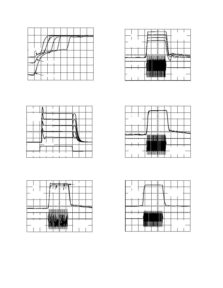
Figure 3. Large Signal RSSI Pulse Response with
C
L
= 100 pF and R
L
= 100
, 154
, and 200
≠Typical Performance Characteristics
100ns PER
HORIZONTAL
DIVISION
GND REFERENCE
INPUT
500mV PER
VERTICAL
DIVISION
V
OUT
500mV PER
VERTICAL
DIVISION
≠3dBV INPUT
LEVEL SHOWN
HERE
Figure 4. RSSI Pulse Response with R
L
= 402
and C
L
=
68 pF, for Inputs Stepped from Zero to ≠33 dBV, ≠23 dBV,
≠13 dBV, and ≠3 dBV
100ns PER
HORIZONTAL
DIVISION
GND REFERENCE
INPUT
500mV PER
VERTICAL
DIVISION
V
OUT
CURVES
OVERLAP
500mV PER
VERTICAL
DIVISION
Figure 5. Large Signal RSSI Pulse Response with
R
L
= 100
and C
L
= 33 pF, 68 pF and 100 pF
20mV PER
VERTICAL
DIVISION
100ns PER
HORIZONTAL
DIVISION
INPUT
V
OUT
200mV PER
VERTICAL
DIVISION
GND REFERENCE
Figure 6. Small Signal RSSI Pulse Response with R
L
= 50
and Back Termination of 50
(Total Load = 100
)
AD8310
≠5≠
REV. A
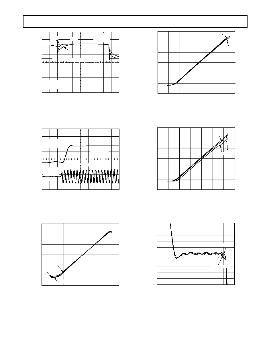
50 s PER
HORIZONTAL
DIVISION
500mV PER
VERTICAL
DIVISION
V
OUT
0.01 F
100pF
3300pF
GROUND REFERENCE
Figure 7. Small Signal AC Response of RSSI Output with
External BFIN Capacitance of 100 pF, 3300 pF and 0.01
µ
F
25ns PER
HORIZONTAL
DIVISION
GROUND REFERENCE
INPUT
500mV PER
VERTICAL
DIVISION
10mV PER
VERTICAL
DIVISION
V
OUT
Figure 8. Small Signal RSSI Pulse Response with
R
L
= 402
and C
L
= 68 pF
INPUT LEVEL ≠ dBV
3.0
0
≠120
20
≠100
(≠87dBm)
RSSI OUTPUT ≠ V
≠80
≠60
≠40
≠20
0
(+13dBm)
2.5
2.0
1.5
1.0
0.5
T
A
= +85 C
T
A
= +25 C
T
A
= ≠40 C
Figure 9. RSSI Output vs. Input Level, 100 MHz Sine Input
at T
A
= ≠40
∞
C, +25
∞
C and +85
∞
C, Single-Ended Input
INPUT LEVEL ≠ dBV
3.0
≠120
≠100
(≠87dBm)
RSSI OUTPUT ≠ V
≠80
≠60
≠40
≠20
0
(+13dBm)
20
2.5
2.0
1.5
1.0
0.5
0
10MHz
50MHz
100MHz
Figure 10. RSSI Output vs. Input Level at T
A
= 25
∞
C for
Frequencies of 10 MHz, 50 MHz, and 100 MHz
INPUT LEVEL ≠ dBV
3.0
0
≠120
20
≠100
(≠87dBm)
RSSI OUTPUT ≠ V
≠80
≠60
≠40
≠20
0
(+13dBm)
2.5
2.0
1.5
1.0
0.5
200MHz
300MHz
440MHz
Figure 11. RSSI Output vs. Input Level at T
A
= 25
∞
C for
Frequencies of 200 MHz, 300 MHz, and 440 MHz
INPUT LEVEL ≠ dBV
5
≠5
≠120
20
≠100
(≠87dBm)
ERROR ≠ dB
≠80
≠60
≠40
≠20
0
(+13dBm)
4
≠1
≠2
≠3
≠4
2
0
3
1
T
A
= +85 C
T
A
= +25 C
T
A
= ≠40 C
Figure 12. Log Linearity of RSSI Output vs. Input Level,
100 MHz Sine Input at T
A
= ≠40
∞
C, +25
∞
C and +85
∞
C
AD8310
≠6≠
REV. A
INPUT LEVEL ≠ dBV
5
≠5
≠120
20
≠100
(≠87dBm)
ERROR ≠ dB
≠80
≠60
≠40
≠20
0
(+13dBm)
4
≠1
≠2
≠3
≠4
2
0
3
1
10MHz
50MHz
100MHz
Figure 13. Log Linearity of RSSI Output vs. Input Level,
at T
A
= 25
∞
C, for Frequencies of 10 MHz, 50 MHz and
100 MHz
INPUT LEVEL ≠ dBV
5
≠5
≠120
20
≠100
(≠87dBm)
ERROR ≠ dB
≠80
≠60
≠40
≠20
0
(+13dBm)
4
≠1
≠2
≠3
≠4
2
0
3
1
200MHz
300MHz
440MHz
Figure 14. Log Linearity of RSSI Output vs. Input Level at
T
A
= 25
∞
C for Frequencies of 200 MHz, 300 MHz and 440 MHz
FREQUENCY ≠ MHz
30
29
20
1
1000
10
RSSI SLOPE ≠ mV/dB
100
24
23
22
21
26
25
28
27
Figure 15. RSSI Slope vs. Frequency
FREQUENCY ≠ MHz
≠99
≠101
≠119
1
1000
10
RSSI INTERCEPT ≠ dBV
100
≠111
≠113
≠115
≠117
≠107
≠109
≠103
≠105
Figure 16. RSSI Intercept vs. Frequency
SLOPE ≠ mV/dB
30
10
0
21.5
22.0
COUNT
5
25
20
15
22.5
23.0
23.5
24.0
24.5
35
40
NORMAL
(23.6584,
0.308728)
Figure 17. Transfer Slope Distribution, V
S
= 5 V,
Frequency = 100 MHz, 25
∞
C
INTERCEPT ≠ dBV
12
4
0
≠115
≠113
COUNT
2
10
8
6
14
16
NORMAL
(≠107.6338,
2.36064)
≠111
≠109
≠107
≠105
≠103
≠101
≠99
≠97
18
20
22
24
Figure 18. Intercept Distribution V
S
= 5 V, Frequency
= 100 MHz, 25
∞
C
AD8310
≠7≠
REV. A
GENERAL THEORY
Logarithmic amplifiers perform a more complex operation than
that of classical linear amplifiers, and their circuitry is significantly
different. A good grasp of what log amps do, and how they do
it, will avoid many pitfalls in their application. For a compete
discussion of the theory, refer to the AD8307 data sheet.
The essential purpose of a log amp is not to amplify, though
amplification is needed internally, but to compress a signal of wide
dynamic range to its decibel equivalent. It is thus a measurement
device. A better term might be "logarithmic converter," since
the function is the conversion of a signal from one domain of
representation to another, via a precise nonlinear transformation:
V
OUT
= V
Y
log (V
IN
/V
X
)
(1)
where V
OUT
is the output voltage, V
Y
is called the "slope voltage,"
the logarithm is usually taken to base-ten (in which case V
Y
is
also the "volts-per-decade"), V
IN
is the input voltage, and V
X
is
called the "intercept voltage." Log amps implicitly require two
references, here V
X
and V
Y
, which determine the scaling of the
circuit. The accuracy of a log amp cannot be any better than the
accuracy of its scaling references. In the AD8310, these are provided
by a band-gap reference.
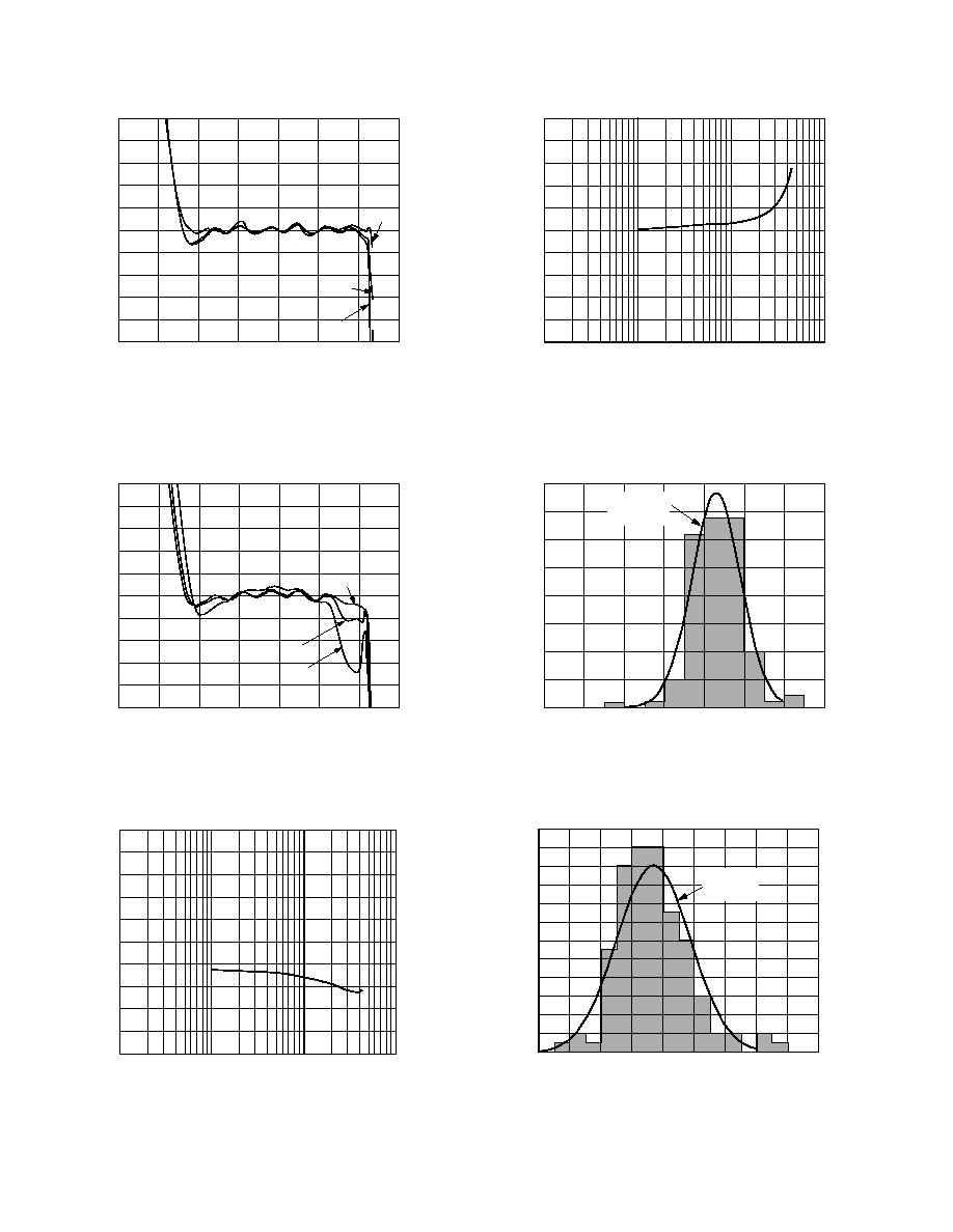
V
OUT
5V
Y
4V
Y
3V
Y
2V
Y
V
Y
≠2V
Y
V
OUT
= 0
LOG V
IN
V
SHIFT
LOWER INTERCEPT
V
IN
= 10
≠2
V
X
≠40dBc
V
IN
= 10
2
V
X
+40dBc
V
IN
= 10
4
V
X
+80dBc
V
IN
= V
X
0dBc
Figure 19. General Form of the Logarithmic Function
While Equation 1, plotted in Figure 19, is fundamentally correct, a
different formula is appropriate for specifying the calibration
attributes or demodulating log amps like the AD8310, operating
in RF applications with a sine wave input:
V
OUT
= V
SLOPE
(P
IN
≠ P
0
)
(2)
Here, V
OUT
is the demodulated and filtered baseband ("video"
or "RSSI") output, V
SLOPE
is the logarithmic slope, now expressed
in volts/dB (25 mV/dB for the AD8310), P
IN
is the input power,
expressed in decibels relative to some reference power level and
is P
0
the logarithmic intercept, expressed in decibels relative to
the same reference level. A widely used reference in RF systems
is decibels above 1 mW in 50
, a level of 0 dBm. Note that the
quantity (P
IN
≠P
0
) is just dB. The logarithmic function disappears
from the formula because the conversion has already been implic-
itly performed in stating the input in decibels. This is strictly a
concession to popular convention: log amps manifestly do not
respond to power (tacitly "power absorbed at the input"), but,
rather, to input voltage. The input is specified in dBV (decibels
with respect to 1 V rms) throughout this data sheet. This is more
precise, although still incomplete, since the signal waveform is
also involved. Since many users specify RF signals in terms of
power--usually in dBm/50
--we also use this convention in
specifying the performance of the AD8310.
Progressive Compression
High-speed high-dynamic range log amps use a cascade of non-
linear amplifier cells to generate the logarithmic function as a
series of contiguous segments, a type of piecewise-linear tech-
nique. The AD8310 employs six cells in its main signal path each
having a small-signal gain of 14.3 dB (
◊
5.2) and a ≠3 dB band-
width of about 900 MHz; the overall gain is about 20,000 (86 dB)
and the overall bandwidth of the chain is some 500 MHz, resulting
in a gain-bandwidth product (GBW) of 10,000 GHz, about a
million times that of a typical op amp. This very high GBW is
essential to accurate operation under small-signal conditions
and at high frequencies. The AD8310 exhibits a logarithmic
response down to inputs as small as 40
µ
V at 440 MHz.
Progressive compression log amps either provide a baseband
"video" response or they accept an RF input and demodulate
this signal to develop an output that is essentially the envelope
of the input represented on a logarithmic or decibel scale. The
AD8310 is the latter kind. Demodulation is performed in a
total of nine detector cells, six of which are associated with
the amplifier stages and three are passive detectors that receive a
progressively-attenuated fraction of the full input. The maximum
signal frequency can be 440 MHz but, since all the gain stages
are dc-coupled, operation at very low frequencies is possible.
Slope and Intercept Calibration
All monolithic log amps from Analog Devices use precision
design techniques to control the logarithmic slope and intercept.
The primary source of this calibration is a pair of accurate voltage
references, that provide supply- and temperature-independent
scaling. The slope is set to 24 mV/dB by the bias chosen for the
detector cells and the subsequent gain of the post-detector output
interface. With this slope, the full 95 dB dynamic range can
easily be accommodated within the output swing capacity when
operating from a 2.7 V supply. Intercept positioning at ≠108 dBV
(≠95 dBm re 50
) has likewise been chosen to provide an output
centered in the available voltage range.
Precise control of the slope and intercept results in a log amp
having stable scaling parameters, making it a true measurement
device as, for example, a calibrated Received Signal Strength
Indicator (RSSI). In this application, the input waveform is
invariably sinusoidal. The input level is correctly specified in
dBV. It may alternatively be stated as an equivalent power, in
dBm, but here we must step carefully, since it is essential to specify
the impedance in which this power is presumed to be measured.
In most RF practice, it is common to assume a reference imped-
ance of 50
, in which 0 dBm (1 mW) corresponds to a sinusoidal
amplitude of 316.2 mV (223.6 mV rms). However, the power
metric is only correct when the input impedance is lowered to
50
, either by a termination resistor added across INHI and
INLO, or by the use of a narrow-band matching network.
It cannot be stated too strongly that log amps do not inherently
respond to power, but to the voltage applied to their input. The
AD8310 presents a nominal input impedance much higher than
50
(typically 1 k
at low frequencies). A simple input matching
network can considerably improve the power sensitivity of this
type of log amp. This increases the voltage applied to the input and
AD8310
≠8≠
REV. A
thus alters the intercept. For a 50
reactive match, the voltage
gain is about 4.8 and the whole dynamic range moves down
by 13.6 dB. Finally, note that the effective intercept is function of
waveform. For example, a square-wave input will read 6 dB
higher than a sine wave of the same amplitude, and a Gaussian
noise input 0.5 dB higher than a sine wave of the same rms value.
Offset Control
In a monolithic log amp, direct-coupling is used between the
stages for several reasons. First, it avoids the need for coupling
capacitors, which may typically have a chip area at least as large
of that of a basic gain cell, thus considerably increasing die size.
Second, the capacitor values predetermine the lowest frequency
at which the log amp can operate; for moderate values, this may
be as high as 30 MHz, limiting the application range. Third, the
parasitic "back-plate" capacitance lowers the bandwidth of the
cell, further limiting the scope of applications.
However, the very high dc gain of a direct-coupled amplifier
raises a practical issue. An offset voltage in the early stages of
the chain is indistinguishable from a "real" signal. If it were as
high as, say, 400
µ
V, it would be 18 dB larger than the smallest
ac signal (50
µ
V), potentially reducing the dynamic range by this
amount. This problem is averted by using a global feedback path
from the last stage to the first, which corrects this offset in a
similar fashion to the dc negative feedback applied around an
op-amp. The high-frequency components of the feedback signal
must, of course, be removed, to prevent a reduction of the HF
gain in the forward path.
An on-chip filter capacitor of 33 pF provides sufficient suppression
of HF feedback to allow operation above 1 MHz. (The ≠3 dB
point in the high-pass response is at 2 MHz, but the usable range
extends well below this frequency). To further lower the frequency
range, an external capacitor may be added at Pin OFLT. For
example, 300 pF lowers it by a factor of ten; operation at low
audio frequencies requires a capacitor of about 1
µ
F. Note that
this filter has no effect for input levels well above the offset volt-
age, where the frequency range would extend down to dc (for
a signal applied directly to the input pins). The dc offset can
optionally be nulled by adjusting the voltage on the OFLT pin
(see Applications).
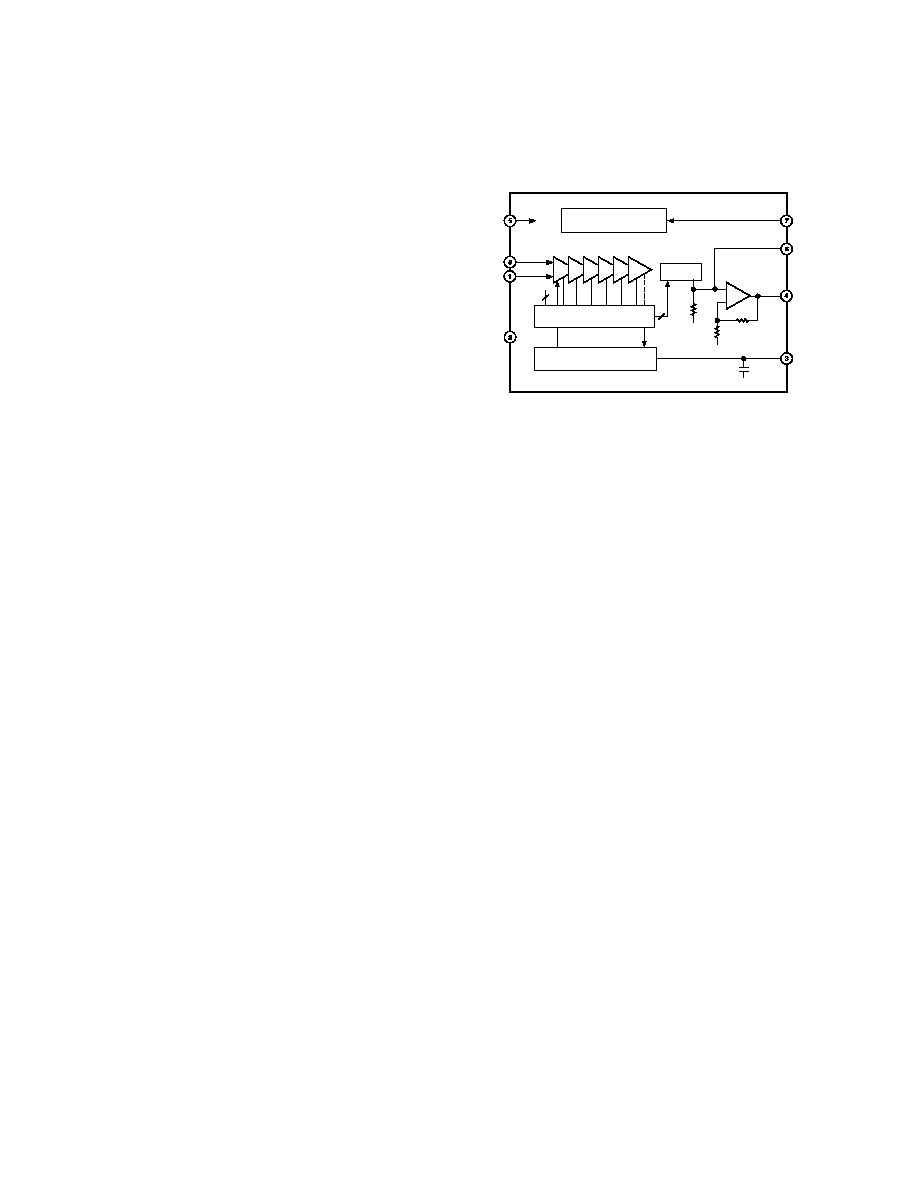
PRODUCT OVERVIEW
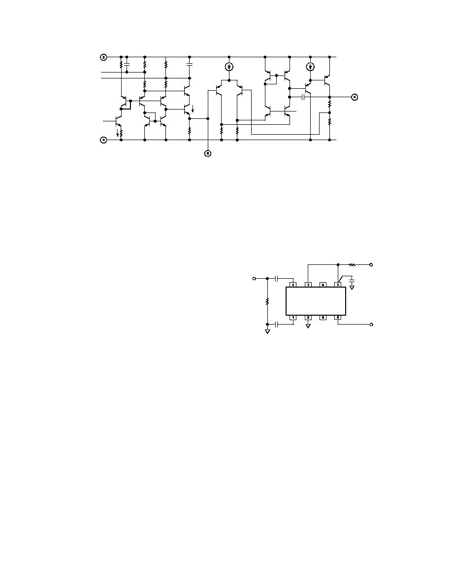
The AD8310 comprises six main amplifier/limiter stages. These
six cells, and their and associated g
m
-styled full-wave detectors,
handle the lower two-thirds of the dynamic range. Three "top-end"
detectors, placed at 14.3 dB taps on a passive attenuator, handle
the upper third of the 95 dB range. The first amplifier stage
provides a low-noise spectral-density (1.28 nV/
Hz). Biasing for
these cells is provided by two references: one determines their gain;
the other is a bandgap circuit that determines the logarithmic
slope, and stabilizes it against supply and temperature variations.
The AD8310 may be enabled/disabled by a CMOS-compatible
level at ENBL (Pin 7).
The differential current-mode outputs of the nine detectors are
summed and then converted to single-sided form, nominally scaled
2
µ
A/dB. The output voltage is developed by applying this current
to 3 k
load resistor, followed by a high-speed gain-of-four
buffer amplifier, resulting in a logarithmic slope of 24 mV/dB
(i.e., 480 mV/decade) at VOUT (Pin 4). The unbuffered voltage
can be accessed at BFIN (Pin 6), allowing certain functional
modifications, including the addition of an external post-
demodulation filter capacitor, and the alteration or adjustment
of slope and intercept.
+
≠
VPOS
INHI
INLO
COMM
3
8mA
1.0k
BANDGAP REFERENCE
AND BIASING
SIX 14.3dB 900MHz
AMPLIFIER STAGES
NINE DETECTOR CELLS
SPACED 14.3dB
INPUT-OFFSET
COMPENSATION LOOP
2
2 A
/dB
MIRROR
3k
3k
1k
COMM
COMM
COMM
ENBL
BFIN
VOUT
OFLT
ENABLE
BUFFER
INPUT
OUTPUT
OFFSET
FILTER
AD8310
SUPPLY
+INPUT
≠INPUT
COMMON
33pF
Figure 20. Main Features of AD8310
The last gain stage also includes an offset-sensing cell. This
generates a bipolarity output current should the main signal
path exhibit an imbalance due to accumulated dc offsets. This
current is integrated by an on-chip capacitor, which may be
increased in value by an off-chip component, at OFLT (Pin
3). The resulting voltage is used to null the offset at the output
of the first stage. Since it does not involve the signal input con-
nections, whose ac coupling capacitors otherwise introduce a
second pole in the feedback path, the stability of the offset
correction loop is assured.
The AD8310 is built on an advanced dielectrically-isolated
complementary bipolar process. In the following interface
diagrams, resistors denoted with an uppercase "R" are thin-film
resistors having a low temperature-coefficient of resistance
(TCR) and high linearity under large-signal conditions. Their
absolute tolerance will typically be within
±
20%. Similarly,
capacitors denoted using an uppercase "C," have a typical
tolerance of
±
15% and essentially zero temperature or voltage
sensitivity. Most interfaces have additional small junction
capacitances associated with them, due to active devices or ESD
protection; these may be neither accurate nor stable. Component
numbering in each of these interface diagrams is local.
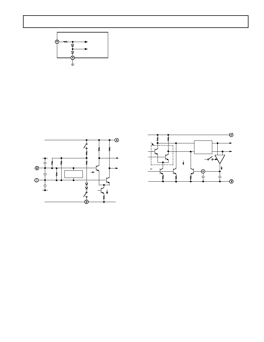
Enable Interface
The chip-enable interface is shown in Figure 21. The currents
in the diode-connected transistors control the turn-on and turn-
off states of the band-gap reference and the bias generator, and
are a maximum of 100
µ
A when ENBL is taken to 5 V, under
worst-case conditions. For voltages below 1 V, the AD8310 will
be disabled, and consume a sleep current of under 1
µ
A; tied to
the supply, or a voltage above 2 V, it will be fully enabled. The
internal bias circuitry is very fast (typically <100 ns for either
OFF or ON). In practice, however, the latency period before the
log amp exhibits its full dynamic range is more likely to be lim-
ited by factors relating to the use of ac-coupling at the input or
the settling of the offset-control loop (see following sections).
AD8310
≠9≠
REV. A
COMM
ENBL
40k
TO BIAS
STAGES
AD8310
Figure 21. ENABLE Interface
Input Interface
Figure 22 shows the essentials of the input interface. C
P
and C
M
are parasitic capacitances; C
D
is the differential input capacitance,
largely due to Q1 and Q2. In most applications both input pins
are ac-coupled. The switches S close when Enable is asserted.
When disabled, bias current I
E
is shut off, and the inputs float;
thus, the coupling capacitors remain charged. If the log amp is
disabled for long periods, small leakage currents will discharge
these capacitors. Then, if they are poorly matched, charging
currents at power-up can generate a transient input voltage that
may block the lower reaches of the dynamic range until it has
become much less than the signal.
TOP-END
DETECTORS
COM
INHI
INLO
C
P
C
D
C
M
COM
4k
~3k
125
6k
6k
2k
TYP 2.2V FOR
3V SUPPLY,
3.2V AT 5V
S
S
VPOS
COMM
I
E
2.4mA
Q1
Q2
Figure 22. Signal Input Interface
A single-sided signal may be applied via a blocking capacitor to
either Pin 1 or 8, with the other pin ac-coupled to ground. Under
these conditions, the largest input signal that can be handled is
0 dBV (a sine amplitude of 1.4 V) when using a 3 V supply; a
+5 dBV input (2.5 V amplitude) may be handled with a 5 V
supply. When using a fully-balanced drive this maximum input
level is permissible for supply voltages as low as 2.7 V. Above
10 MHz, this is easily achieved using an LC matching network.
Such a network, having an inductor at the input, usefully elimi-
nates the input transient noted above.
Occasionally, it may be desirable to use the dc-coupled potential
of the AD8310, in baseband applications. The main challenge
here is to present the signal at the elevated common-mode input
level, which may require the use of low-noise, low-offset buffer
amplifiers. In some cases, it may be possible to use dual supplies
of
±
3 V, which allows the input pins to operate at ground poten-
tial. The output, which is internally referenced to the COMM
pin (now at ≠3 V), may be positioned back to ground level, with
essentially no sensitivity to the particular value of the negative
supply.
Offset Interface
The input-referred dc offsets in the signal path are nulled via the
interface associated with Pin 3, shown in Figure 23. Q1 and Q2
are the first-stage input transistors, having slightly unbalanced
load resistors, resulting in a deliberate offset voltage of about
1.5 mV referred to the input pins. Q3 generates a small current
to null this error, dependent on the voltage at the OFLT pin.
When Q1 and Q2 are perfectly matched this voltage is about
1.75 V; in practice, it will range from approximately 1 V to 2.5 V
for an input-referred offset of
±
1.5 mV.
48k
125
MAIN GAIN
STAGES
Q2
Q1
Q3
16 A AT
BALANCE
Q4
g
m
S
AVERAGE
ERROR
CURRENT
OFLT
TO LAST
DETECTOR
C
OFLT
33pF
COMM
VPOS
36k
INPUT
STAGE
BIAS, 1.2V
Figure 23. Offset Interface and Offset-Nulling Path
In normal operation using an ac-coupled input signal, the OFLT
pin should be left unconnected. The g
m
cell, which is gated off
when the chip is disabled, converts a residual offset (sensed at a
point near the end of the cascade of amplifiers) to a current.
This is integrated by the on-chip capacitor C
HP
, plus any added
external capacitance C
OFLT
, to generate the voltage that is applied
back to the input stage in the polarity needed to null the output
offset. From a small-signal perspective, this feedback alters the
response of the amplifier, which exhibits a zero in its ac transfer
function, resulting in a closed-loop high-pass ≠3 dB corner at
about 2 MHz. An external capacitor will lower the high-pass
corner to arbitrarily low frequencies; using 1
µ
F, the 3 dB corner
is at 60 Hz.
AD8310
≠10≠
REV. A
0.2pF
BIAS
3k
1k
4k
4k
R1
3k
2 A/dB
0.4pF
1.25k
1.25k
1.25k
1.25k
BFIN
0.4pF
60 A
VPOS
COMM
BIAS
LGP
LGN
FROM ALL
DETECTORS
VOUT
Figure 24. Simplified Output Interface
Output Interface
The nine detectors generate differential currents, having an
average value that is dependent on the signal input level, plus a
fluctuation at twice the input frequency. These are summed at
nodes LGP and LGN in Figure 24. Further currents are added at
these nodes, to position the intercept, by slightly raising the output
for zero input, and to provide temperature compensation.
For zero-signal conditions, all the detector output currents are
equal. For a finite input, of either polarity, their difference is
converted by the output interface to a single-sided unipolar
current, nominally scaled 2
µ
A/dB (40
µ
A/decade), at the output
pin BFIN. An on-chip resistor, R1, of ~3 k
, converts this
current to a voltage of 6 mV/dB. This is then amplified by a
factor of four in the output buffer, which can drive a current of
up to 25 mA in a grounded load resistor. The overall rise-time
of the AD8310 is under 15 ns; there is also a delay time of about
6 ns when the log amp is driven by an RF burst, starting at zero
amplitude. When driving capacitive loads, it is desirable to add a
low value of load resistor to speed up the return to the baseline;
the buffer is stable for loads of a least 100 pF. The output band-
width may be lowered by adding a grounded capacitor at BFIN.
The time-constant of the resulting single-pole filter is formed
with the 3 k
internal load resistor (having a tolerance of 20%);
thus, to set the ≠3 dB frequency to 20 kHz, use a capacitor of
2.7 nF. Using 2.7
µ
F, the filter corner is at 20 Hz.
USING THE AD8310
The AD8310 has very high gain and bandwidth. Consequently,
it is susceptible to all signals that appear at the input terminals
within a very broad frequency range. Without the benefit of
filtering, these will be quite indistinguishable from the "wanted"
signal, and will have the effect of raising the apparent noise floor
(that is, lowering the useful dynamic range). For example, while
the signal of interest may be an IF of 50 MHz, any of the following
could easily be larger than the IF signal at the lower extremities of
its dynamic range: a few hundred microvolts of 60 Hz hum,
picked up due to poor grounding techniques; spurious coupling
from a digital clock source on the same PC board; local radio
stations; etc. Careful shielding and supply decoupling is therefore
essential. A ground-plane should be used to provide a low-
impedance connection to the common pin COMM, for the
decoupling capacitor(s) used at VPOS, and for the output ground.
Basic Connections
Figure 25 shows the connections needed for most applications.
A supply voltage between 2.7 V and 5.5 V is applied to VPOS
and is decoupled using a 0.01
µ
F capacitor close to the pin.
Optionally, a small series resistor can be placed in the power
line to give additional filtering of power supply noise. The
ENBL input, which has a threshold of approximately 1.3 V (see
Figure 1), should be tied to VPOS when this feature is not needed.
V
S
(2.7≠5.5V)
C2
0.01 F
52.3
NC = NO CONNECT
C1
0.01 F
C4
0.01 F
NC
NC
INHI ENBL BFIN VPOS
INLO COMM OFLT VOUT
AD8310
4.7
OPTIONAL
V
OUT
(RSSI)
SIGNAL
INPUT
Figure 25. Basic Connections
While the AD8310's input can be driven differentially, the input
signal will, in general, be single-ended. C1 is tied to ground and
the input signal is coupled in through C2. Capacitors C1 and
C2 should have the same value, to minimize start-up transients
when the enable feature is used; otherwise, their values need not
be equal.
The 52.3
resistor combines with the 1.1 k
input impedance
of the AD8310 to yield a simple broadband 50
input match.
An input matching network can also be used (see Input Matching
section).
The coupling time-constant 50
◊
C
C
/2, forms a high-pass corner
with a 3 dB attenuation at f
HP
= 1/(
◊
50
◊
C
C
), where C1 =
C2 = C
C
. In high-frequency applications, f
HP
should be as large
as possible, in order to minimize the coupling of unwanted low-
frequency signals. In low-frequency applications, a simple RC
network forming a low-pass filter should be added at the input
for similar reasons. This should generally be placed at the gen-
erator side of the coupling capacitors, thus lowering the required
capacitance value for a given high-pass corner frequency.
AD8310
≠11≠
REV. A
V
S
(2.7≠5.5V)
C2
0.01 F
52.3
NC = NO CONNECT
C1
0.01 F
C4
0.01 F
NC
NC
INHI ENBL BFIN VPOS
INLO COMM OFLT VOUT
AD8310
4.7
OPTIONAL
V
OUT
(RSSI)
SIGNAL
INPUT
4.7
GENERATOR
COMMON
BOARD-LEVEL
GROUND
Figure 26. Connections for Isolation of "Source" Ground
from Device Ground
In applications where the ground plane may not be an equipoten-
tial (possibly due to noise in the ground plane), the "low" input
of an unbalanced source should generally be ac-coupled through
a separate connection the "low" associated with the source.
Furthermore, it is good practice in such situations to break the
ground loop by inserting a small resistance to ground in the "low"
side of the input connector (Figure 26).
Figure 27 shows the output versus the input level for sine
inputs at 10 MHz, 50 MHz, and 100 MHz; Figure 28 shows
the logarithmic conformance under the same conditions.
INPUT LEVEL ≠ dBV
3.0
≠120
≠100
OUTPUT ≠ V
≠80
≠60
≠40
≠20
0
(+13dBm)
20
2.5
2.0
1.5
1.0
0.5
0
10MHz
50MHz
100MHz
INTERCEPT
(≠87dBm)
Figure 27. Output vs. Input Level at 10 MHz, 50 MHz, and
100 MHz
INPUT LEVEL ≠ dBV
5
≠5
≠120
20
≠100
(≠87dBm)
ERROR ≠ dB
≠80
≠60
≠40
≠20
0
(+13dBm)
4
≠1
≠2
≠3
≠4
2
0
3
1
10MHz
50MHz
100MHz
3dB DYNAMIC RANGE
1dB DYNAMIC RANGE
Figure 28. Log-Conformance Errors vs. Input Level at
10 MHz, 50 MHz, and 100 MHz
Transfer Function in Terms of Slope and Intercept
The transfer function of the AD8310 is characterized in terms of
its Slope and Intercept. The logarithmic slope is defined as the
change in the RSSI output voltage for a 1 dB change at the input.
For the AD8310, slope is nominally 24 mV/dB. Therefore, a 10 dB
change at the input results in a change at the output of approxi-
mately 240 mV. The plot of Log-Conformance shows the range
over which the device maintains its constant slope. The dynamic
range of the log amp is defined as the range over which the slope
remains within a certain error band, usually
±
1 dB or
±
3 dB. In
Figure 28, for example, the
±
1 dB dynamic range is approximately
95 dB (from +4 dBV to ≠91 dBV).
The intercept is the point at which the extrapolated linear response
would intersect the horizontal axis (see Figure 27). For the
AD8310 the intercept is calibrated to be ≠108 dBV (≠95 dBm).
Using the slope and intercept, the output voltage can be calcu-
lated for any input level within the specified input range using
the equation:
V
OUT
= V
SLOPE
◊
(P
IN
≠ P
0
)
where V
OUT
is the demodulated and filtered RSSI output, V
SLOPE
is the logarithmic slope, expressed in V/dB, P
IN
is the input signal,
expressed in decibels relative to some reference level (either
dBm or dBV in this case) and P
0
is the logarithmic intercept, ex-
pressed in decibels relative to the same reference level.
For example, for an input level of ≠33 dBV (≠20 dBm), the out-
put voltage will be
V
OUT
= 0.024 V/dB
◊
(≠33 dBV ≠ (≠108 dBV)) = 1.8 V
dBV vs. dBm
The most widely used convention in RF systems is to specify
power in dBm, that is, decibels above 1 mW in 50
. Specifi-
cation of log amp input level in terms of power is strictly a
concession to popular convention; they do not respond to power
(tacitly "power absorbed at the input"), but to the input voltage.
The use of dBV, defined as decibels with respect to a 1 V rms sine
wave, is more precise, although this is still not unambiguous
because waveform is also involved in the response of a log amp,
which, for a complex input (such as a CDMA signal) will not
follow the rms value exactly. Since most users specify RF signals
in terms of power--more specifically, in dBm/50
--we use both
dBV and dBm in specifying the performance of the AD8310,
showing equivalent dBm levels for the special case of a 50
environment. Values in dBV are converted to dBm re 50
by
adding 13 dB.
Effect of Waveform Type on Intercept
Input signals of equal rms power, but differing crest factors, will
produce different results at the log amp's output.
Differing signal waveforms shift the effective value of the inter-
cept. Graphically, this looks like a vertical shift in the log amp's
transfer function. The logarithmic slope, however, is not affected.
For example, consider the case of the AD8310 being alternately
fed by an unmodulated sine wave and by a single CDMA channel
of the same rms power. The output voltage will differ by the
equivalent of 3.55 dB (71 mV) over the complete dynamic range
of the device (the output for the CDMA input being lower).
AD8310
≠12≠
REV. A
Table I shows the correction factors that should be applied to
measure the rms signal strength of a various signal types. A sine
wave input is used as a reference. To measure the rms power of
a square wave, for example, the mV equivalent of the dB value
given in the table (24 mV/dB times 3.01 dB) should be subtracted
from the output voltage of the AD8310.
Table I. Correction for Signals with Differing Crest Factors
Correction Factor
(Add to Measured Input
Signal Type
Level)
Sine Wave
0 dB
Square Wave or DC
≠3.01 dB
Triangular Wave
0.9 dB
GSM Channel (All Time Slots On)
0.55 dB
CDMA Channel (Forward Link, 9
Channels On)
3.55 dB
CDMA Channel (Reverse Link)
0.5 dB
PDC Channel (All Time Slots On) 0.58 dB
Input Matching
Where higher sensitivity is required, an input matching net-
work is useful. Using a transformer to achieve the impedance
transformation also eliminates the need for coupling capacitors,
lowers the offset voltage generated directly at the input, and
balances the drive amplitude to INLO and INHI. The choice of
turns ratio will depend somewhat on the frequency. At frequencies
below 50 MHz, the reactance of the input capacitance is much
higher than the real part of the input impedance. In this frequency
range, a turns ratio of about 1:4.8 will lower the input impedance
to 50
while raising the input voltage, and thus lowering the
effect of the short circuit noise voltage by the same factor. The
intercept will also be lowered by the turns ratio; for a 50
match, it will be reduced by 20 log
10
(4.8) or 13.6 dB. The total
noise will be reduced by a somewhat smaller factor because
there will be a small contribution from the input noise current.
Narrow-Band Matching
Transformer coupling is useful in broadband applications. How-
ever, a magnetically-coupled transformer may not be convenient
in some situations. At high frequencies, it is often preferable to
use a narrow-band matching network, as shown in Figure 29.
This has several advantages. The same voltage gain is achieved,
providing increased sensitivity, but now a measure of selectively
is also introduced. The component count is low: two capacitors
and an inexpensive chip inductor. Further, by making these
capacitors unequal the amplitudes at INP and INM may be
equalized when driving from a single-sided source; that is, the
network also serves as a balun. Figure 30 shows the response for
a center frequency of 100 MHz; note the very high attenuation
at low frequencies. The high-frequency attenuation is due to the
input capacitance of the log amp.
C1
C2
INHI
INLO
AD8310
SIGNAL
INPUT
L
M
Figure 29. Reactive Matching Network
FREQUENCY ≠ MHz
14
4
≠1
60
150
80
DECIBELS
100
110
130
3
2
1
0
70
90
120
140
INPUT
GAIN
9
8
7
6
5
13
12
11
10
Figure 30. Response of 100 MHz Matching Network
Table II. Narrow-Band Matching Values
F
C
Z
IN
C1
C2
L
M
Voltage
MHz
pF
pF
nH
Gain (dB)
10
45
160
150
3300
13.3
20
44
82
75
1600
13.4
50
46
30
27
680
13.4
100
50
15
13
270
13.4
150
57
10
8.2
220
13.2
200
57
7.5
6.8
150
12.8
250
50
6.2
5.6
100
12.3
500
54
3.9
3.3
39
10.9
10
103
100
91
5600
10.4
20
102
51
43
2700
10.4
50
99
22
18
1000
10.6
100
98
11
9.1
430
10.5
150
101
7.5
6.2
260
10.3
200
95
5.6
4.7
180
10.3
250
92
4.3
3.9
130
9.9
500
114
2.2
2.0
47
6.8
AD8310
≠13≠
REV. A
General Matching Procedure
For other center frequencies and source impedances, the following
method can be used to calculate the basic matching parameters.
Step 1: Tune Out C
IN
At a center frequency f
C
, the shunt impedance of the input
capacitance C
IN
can be made to disappear by resonating with a
temporary inductor L
IN
, whose value is given by
L
w C
IN
IN
=
1
2
when C
IN
= 1.4 pF. For example, at f
C
= 100 MHz, L
IN
= 1.8
µ
H.
Step 2: Calculate C
O
and L
O
Now having a purely resistive input impedance, we can calculate
the nominal coupling elements C
O
and L
O
, using
C
f
R
R
L
R
R
f
O
C
IN
M
O
IN
M
C
=
(
)
=
(
)
1
2
2
;
For the AD8310, R
IN
is 1 k
. Thus, if a match to 50
is needed,
at f
C
= 100 MHz, C
O
must be 7.12 pF and L
O
must be 356 nH.
Step 3: Split C
O
Into Two Parts
Since we wish to provide the fully-balanced form of network
shown in Figure 29, two capacitors C1 = C2
each of nominally
twice C
O
, shown as C
M
in the figure, can be used. This requires
a value of 14.24 pF in this example. Under these conditions, the
voltage amplitudes at INHI and INLO will be similar. A some-
what better balance in the two drives may be achieved when C1
is made slightly larger than C2, which also allows a wider range
of choices in selecting from standard values. For example,
capacitors of C1 = 15 pF and C2 = 13 pF may be used (making
C
O
= 6.96 pF).
Step 4: Calculate L
M
The matching inductor required to provide both L
IN
and L
O
is
just the parallel combination of these:
L
M
= L
IN
L
O
/(L
IN
+ L
O
)
With L
IN
= 1.8
µ
H and L
O
= 356 nH, the value of L
M
to com-
plete this example of a match of 50
at 100 MHz is 297.2 nH.
The nearest standard value of 270 nH may be used with only a
slight loss of matching accuracy. The voltage gain at resonance
depends only on the ratio of impedances, as given by
GAIN
R
R
R
R
IN
S
IN
S
=
=
20
10
log
log
Slope and Intercept Adjustments
Where system (i.e., software) calibration is not available, the
adjustments shown in Figure 31 can be used, either singly or in
combination, to trim the absolute accuracy of the AD8310. The
log slope may be raised or lowered by VR1; the values shown
provide a calibration range of
±
10% (22.6 mV/dB to 27.4 mV/dB),
which includes full allowance for the variability in the value of
the internal resistances. The adjustment may be made by alter-
nately applying two fixed input levels, provided by an accurate
signal generator, spaced over the central portion of the dynamic
range, for example ≠60 dBV and ≠20 dBV.
Alternatively, an AM-modulated signal, at about the center of
the dynamic range, may be used. For a modulation depth M,
expressed as a fraction, the decibel range between the peaks and
troughs over one cycle of the modulation period is given by
dB
M
M
=
+
20
1
1
10
log
≠
(3)
For example., using a generator output of ≠40 dBm with a 70%
modulation depth (M = 0.7), the decibel range is 15 dB, as the
signal varies from ≠47.5 dBm to ≠32.5 dBm.
The log intercept is adjustable by VR2 over a ≠3 dB range with
the component values shown. VR2 is adjusted while applying an
accurately-known CW signal, preferably near the lower end of the
dynamic range, in order to minimize the effect of any residual
uncertainty in the slope. For example, to position the intercept
to ≠80 dBm, a test level of ≠65 dBm may be applied and VR2
adjusted to produce a dc output of 15 dB above zero at 24 mV/dB,
which is 360 mV.
+V
S
(2.7≠5.5V)
0.01 F
52.3
NC = NO CONNECT
C1
0.01 F
NC
INHI ENBL BFIN VPOS
INLO COMM OFLT VOUT
AD8310
4.7
V
OUT
(RSSI)
SIGNAL
INPUT
10k
C2
0.01 F
25k
VR1
10k
R
S
VR2
100k
FOR V
POS
= 3V, R
S
= 500k
FOR V
POS
= 5V, R
S
= 850k
24mV/dB 10%
1
2
3
4
8
7
6
5
Figure 31. Slope and Intercept Adjustments
Increasing the Slope to a Fixed Value
It is also possible to increase the slope to a new fixed value and
thus increase the change in output for each decibel of input
change. A common example of this is the need to "map" the
output swing of the AD8310 into the input range of an analog-
to-digital converter (ADC) with a rail-to-rail input swing.
Alternatively, a situation might arise, when only a part of the
total dynamic range is required--say, just 20 dB--in an applica-
tion where the nominal input level is more tightly constrained
and a higher sensitivity to a change in this level is required. Of
course, the maximum output will be limited either by the load
resistance and the maximum output current rating of 25 mA, or
by the supply voltage (see Specifications). The slope may easily
be raised by adding a resistor from VOUT to BFIN as shown in
Figure 32. This alters the gain of the output buffer, by means of
stable positive feedback, from its normal value of four to an
effective value which may be as high as sixteen, corresponding
to a slope of 100 mV/dB. The resistor R
SLOPE
is set according
to the equation
R
k
mV dB
Slope
SLOPE
=
9 22
1
24
.
≠
/
AD8310
≠14≠
REV. A
V
S
(2.7≠5.5V)
0.01 F
52.3
NC = NO CONNECT
C1
0.01 F
NC
INHI ENBL BFIN VPOS
INLO COMM OFLT VOUT
AD8310
4.7
V
OUT
100mV/dB
SIGNAL
INPUT
C2
0.01 F
R
SLOPE
12.1k
1
2
3
4
8
7
6
5
Figure 32. Raising the Slope to 100 mV/dB
Output Filtering
In applications where maximum video bandwidth (and conse-
quently fast rise time) is desired, it is essential that the BFIN pin
be left unconnected and free of any stray capacitance.
The nominal output video bandwidth of 25 MHz, can be reduced
by connecting a ground-referenced capacitor (C
FILT
) to the BFIN
pin as shown in Figure 33. This is generally done to reduce output
ripple (at twice the input frequency for a symmetric input wave-
form such as sinusoidal signals).
C
FILT
is selected using the equation
C
FILT
= 1/(2
◊
3 k
◊
Video Bandwidth) ≠2.1 pF
The Video Bandwidth should typically be set at a frequency equal
to about one-tenth the minimum input frequency. This will
ensure that the output ripple of the demodulated log output, which
is at twice the input frequency, will be well filtered.
In many applications of log amps, it may be necessary to lower
the corner frequency of the post-demodulation filtering, in order
to achieve low output ripple while maintaining a rapid response
time to changes in signal level. An example of a four-pole active
filter is shown the AD8307 data sheet.
+4
2 A/dB
3k
V
OUT
BFIN
C
FILT
AD8310
C
FILT
= 1/(2 3k VIDEO BANDWIDTH) ≠ 2.1pF
Figure 33. Lowering the Post-Demodulation Video
Bandwidth
Lowering the High-Pass Corner Frequency of the Offset
Compensation Loop
In normal operation, using an AC-coupled input signal, the
OFLT pin should be left unconnected. Input-referred dc offsets
of about 1.5 mV in the signal path are nulled via an internal
offset control loop. This loop has a high-pass ≠3 dB corner at
about 2 MHz. In low frequency ac-coupled applications, it is
necessary to lower this corner frequency to prevent input signals
from being misinterpreted as offsets. An external capacitor on
OFLT will lower the high-pass corner to arbitrarily low frequencies
(Figure 34). For example, by using 1
µ
F capacitor, the 3 dB
corner will be reduced to 60 Hz.
The corner frequency is set by the equation
F
CORNER
= 1/(2
◊
2625
◊
C
OFLT
)
where C
OFLT
is the capacitor connected to OFLT.
C
OFLT
(SEE TEXT)
AD8310
OFLT
Figure 34. Lowering the High-Pass Corner Frequency of
the Offset Control Loop
APPLICATIONS
The AD8310 is highly versatile and easy to use. Being complete,
it needs only a few external components, and most can be
immediately accommodated by using the simple connections
shown in the preceding section. A few examples of more special-
ized applications are provided here; see also the AD8307 data
sheet for further applications; note the slightly different pinout.
Cable-Driving
The AD8310 is capable of driving a grounded 100
load to 2.5 V,
for a supply voltage of 3 V or greater. If reverse-termination is
required when driving a 50
cable, it should be included in
series with the output, as shown in Figure 35. The slope at the
load will then be 12 mV/dB. In some cases, it may be permis-
sible to operate the cable without a termination at the far end,
in which case the slope will not be lowered. Where a further
increase in slope is desirable, the scheme shown in Figure 32
may be used.
AD8310
VOUT
50
50
Figure 35. Output Response of Cable-Driver Application
DC-Coupled Input
It may occasionally be necessary to provide response to dc
inputs. Since the AD8310 is internally dc-coupled, there is no
fundamental reason why this is precluded. However, there is a
practical constraint, which is that its differential inputs must be
positioned at least 2 V above the COM potential for proper
biasing of the first stage. Usually, the source will be a single-sided
ground-referenced signal, so it will thus be necessary to provide
level-shifting and a single-ended-to-differential conversion to
correctly drive the AD8310's inputs.
Figure 36 shows how a level-shift to midsupply (2.5 V in this
example) and a single-ended-to-differential conversion can be
accomplished using the AD8138 differential amplifier. The four
499
resistors set up a gain of unity. An output common-mode
(or bias) voltage of 2.5 is achieved by applying 2.5 V (from a
supply-referenced resistive divider) to the AD8138's VOCM
pin. The differential outputs of the AD8138 directly drive the
1.1 k
input impedance of the AD8310.
AD8310
≠15≠
REV. A
5V
0.01 F
SIGNAL
INPUT
AD8138
0.1 F
5V
499
499
499
499
10k
0.1 F
5V
10k
NC
INHI ENBL BFIN VPOS
INLO COMM OFLT VOUT
AD8310
V
OUT
1
2
3
4
8
7
6
5
5V
3.01k
1.87k
50
2.5V
NC = NO CONNECT
Figure 36. DC-Coupled Log Amp
It is necessary in this application to trim the offset voltage of
the AD8138. The internal offset compensation circuitry of the
AD8310 is disabled by applying a nominal voltage of around
1.9 V to the OFLF pin. So the trim on the AD8138 is effectively
trimming both devices' offsets. The trim is done by grounding
the circuit's input and slightly varying the gain resistors on the
AD8138's inverting input (a 50
potentiometer is used in this
example) until the voltage on the AD8310's output reaches a
minimum.
After trimming, the lower end of the dynamic range is limited
by the broadband noise at the output of the AD8138, which
is approximately 425
µ
V p-p. A differential low-pass filter may
be added between the AD8138 and the AD8310 when the very
fast pulse response of the circuit is not required.
INPUT LEVEL ≠ mV
0.1
RSSI OUTPUT ≠ V
1
0.7
0.9
1.1
1.3
1.5
1.7
1.9
2.1
10
100
1000
2.3
2.5
2.7
Figure 37. Transfer Function of DC-Coupled Log Amp
Application
Evaluation Board
An evaluation board, carefully laid out and tested to demon-
strate the specified high-speed performance of the AD8310 is
available. Figure 38 shows the schematic of the evaluation board,
which fairly closely follows the basic connections schematic
shown in Figure 25. Connectors INHI, INLO and VOUT are
SMA type; supply and ground are connected to vector pins TP1
and TP1, switches and component settings for different setups
are described in Table III. The layout and silkscreen for the
component side of the board are shown in Figure 39 and Figure
40. For ordering information, please refer to the Ordering Guide.
C2
0.01 F
INHI ENBL BFIN VPOS
INLO COMM OFLT VOUT
AD8310
1
2
3
4
8
7
6
5
C4
0.01 F
C1
0.01 F
R3
52.3
R4
0
R1
0
INHI
INLO
TP2
C7
(OPEN)
(0603 PAD)
W1
W2
C6
(OPEN)
(0603 PAD)
R7
(OPEN)
(0603 PAD)
R6
0
V
OUT
C5
(OPEN, 0805 PAD)
C3
(OPEN)
(0603
PAD)
SW1
A
B
R5
0
TP1
V
S
Figure 38. Evaluation Board Schematic
Figure 39. Layout of Component Side of Evaluation Board
Figure 40. Component Side Silkscreen of Evaluation
Board
≠16≠
C3690≠0≠12/99 (rev. A)
PRINTED IN U.S.A.
AD8310
REV. A
Table III. Evaluation Boards Setup Options
Component
Function
Default Condition
TP1, TP2
Supply and Ground Vector Pins
Not Applicable
SW1
Device Enable: When in Position A, the ENBL pin is connected to +V
S
and the
SW1 = A
AD8310 is in normal operating mode. In Position B, the ENBL pin is connected to
ground putting the device in sleep mode.
R1/R4
SMA Connector Grounds: Connects common of INHI and INLO SMA connectors
R1 = R4 = 0
to ground. Can be used to isolate the generator ground from the evaluation board
ground (see Figure 26).
C1, C2, R2, R3
Input Interface: R3 (52.3
) combines with the AD8310's 1 k
input impedance to
R3 = 52.3
give an overall broadband input impedance of 50
. C1, C2, and the AD8310's input
R2 = 0
impedance combine to set a high-pass input corner of 32 kHz. Alternatively, R3, C1,
C1 = C2 = 0.01
µ
F
and C2 can be replaced by an inductor and matching capacitors to form an input
matching network. See Input Matching section for more detail.
C3
RSSI (Video) Bandwidth Adjust: The addition of C3 (Farads) will lower the RSSI bandwidth
C3 = Open
of the VLOG output according to the equation: C
FILT
= 1/(2
◊
3 k
◊
Video Bandwidth)
≠2.1 pF.
C4, C5, R5
Supply Decoupling: The nominal supply decoupling of 0.01
µ
F (C4) can be augmented by a
C4 = 0.01
µ
F
larger cap in C5. An inductor or small resistor can be placed in R5 for additional decoupling.
C5 = Open, R5 = 0
R6
Output Source Impedance: In cable-driving applications, a resistor (typically 50
or 75
)
R6 = 0
can be placed in R6 to give the circuit a back-terminated output impedance.
W1, W2, C6, R7
Output Loading: Resistors and capacitors can be placed in C6 and R7 to load test V
OUT
.
C6 = R7 = Open
Jumpers W1 and W2 are used to connect/disconnect the loads.
W1 = W2 = Installed
C7
Offset Compensation Loop: A capacitor in C7 will reduce the corner frequency of
C7 = Open
the offset control loop in low frequency applications.
OUTLINE DIMENSIONS
Dimensions shown in inches and (mm).
8-Lead Mini_SO
(RM-8)
0.009 (0.23)
0.005 (0.13)
0.028 (0.70)
0.016 (0.40)
6
0
0.037 (0.95)
0.030 (0.75)
8
5
4
1
0.122 (3.10)
0.114 (2.90)
PIN 1
0.0256 (0.65) BSC
0.122 (3.10)
0.114 (2.90)
0.193
(4.90)
BSC
SEATING
PLANE
0.006 (0.15)
0.002 (0.05)
0.016 (0.40)
0.010 (0.25)
0.043
(1.10)
MAX