 | –≠–ª–µ–∫—Ç—Ä–æ–Ω–Ω—ã–π –∫–æ–º–ø–æ–Ω–µ–Ω—Ç: AD8316 | –°–∫–∞—á–∞—Ç—å:  PDF PDF  ZIP ZIP |
Document Outline
- FEATURES
- APPLICATIONS
- GENERAL DESCRIPTION
- FUNCTIONAL BLOCK DIAGRAM
- SPECIFICATIONS
- ABSOLUTE MAXIMUM RATINGS
- PIN CONFIGURATION
- PIN FUNCTION DESCRIPTIONS
- ORDERING GUIDE
- Typical Performance Characteristics
- GENERAL DESCRIPTION AND THEORY
- Basic Theory
- Controller-Mode Log Amps
- Control Loop Dynamics
- Example
- Practical Loop
- A Note About Power Equivalency
- Basic Connections
- Range on VSET and RF Input
- Transient Response
- Mobile Handset Power Control Example
- Enable and Power-On
- Input Coupling Options
- Using the Chip Scale Package
- EVALUATION BOARD
- OUTLINE DIMENSIONS
- Revision History
REV. C
Information furnished by Analog Devices is believed to be accurate and
reliable. However, no responsibility is assumed by Analog Devices for its
use, nor for any infringements of patents or other rights of third parties that
may result from its use. No license is granted by implication or otherwise
under any patent or patent rights of Analog Devices. Trademarks and
registered trademarks are the property of their respective owners.
One Technology Way, P.O. Box 9106, Norwood, MA 02062-9106, U.S.A.
Tel: 781/329-4700
www.analog.com
Fax: 781/326-8703
© 2004 Analog Devices, Inc. All rights reserved.
AD8316
Dual Output
GSM PA Controller
FEATURES
Complete RF Detector/Controller Function
Selectable Dual Outputs
49 dB Range at 0.9 GHz (≠47.6 dBm to +1.5 dBm re 50 )
Accurate Scaling from 0.1 GHz to 2.5 GHz
Temperature-Stable Linear-in-dB Response
Log Slope of 22 mV/dB
True Integration Function in Control Loop
Low Power: 23 mW at 2.7 V
Power-Down to 11 W
APPLICATIONS
Single-Band, Dual-Band, and Triband Mobile Handsets
(GSM, DCS, PCS, EDGE)
Wireless Terminal Devices
Transmitter Power Control
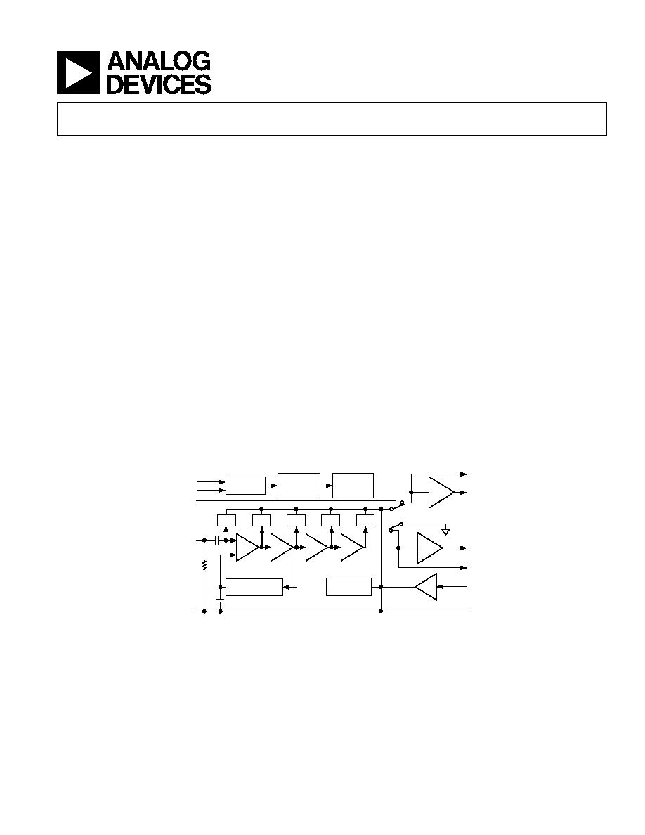
FUNCTIONAL BLOCK DIAGRAM
OUT2
OUT1
FLT1
VSET
FLT2
10dB
COMM
OFFSET
COMPENSATION
RFIN
DET
DET
DET
DET
DET
INTERCEPT
POSITIONING
LOW NOISE
GAIN BIAS
LOW NOISE
BAND GAP
REFERENCE
OUTPUT
ENABLE
DELAY
ENBL
VPOS
BSEL
HI-Z
1.35
HI-Z
V≠I
10dB
10dB
10dB
1.35
GENERAL DESCRIPTION
The AD8316 is a complete, low cost subsystem for the precise
control of dual RF power amplifiers (PAs) operating in the
frequency range 0.1 GHz to 2.5 GHz and over a typical dynamic
range of 50 dB. The device is a dual-output version of the AD8315
and intended for use in dual-band or triband cellular handsets
and other battery-operated wireless devices where a separate
power control signal is required for each band. The logarithmic
amplifier technique provides a much wider measurement range
and better accuracy than is possible using controllers based on
diode detectors. In particular, multiband and multimode cellu-
lar designs can benefit from the temperature-stable (≠30
∞C to
+85
∞C) operation over all cellular telephony frequencies.
Its high sensitivity allows control at low input signal levels, thus
reducing the amount of power that needs to be coupled to the
detector. The selected output, OUT1 or OUT2, has the voltage
range and current drive to directly connect to the gain control
pin of most handset power amplifiers; the deselected output is
pulled low to ensure that the inactive PA remains off. Each
output has a dedicated integrating filter capacitor that allows
separate control loop settings for each PA. OUT1 and OUT2 can
swing from 125 mV above ground to within 100 mV below the
supply voltage. Load currents of up to 12 mA can be supported.
The setpoint control input applied to pin VSET has an operating
range of 0.25 V to 1.4 V. The input resistance of the setpoint
interface is over 100 M
, and the bias current is typically 0.5 µA.
The AD8316 is available in 10-lead MSOP and 16-lead LFCSP
packages and consumes 8.5 mA from a 2.7 V to 5.5 V supply.
When it is powered down, the sleep current is 4
µA.

REV. C
≠2≠
AD8316≠SPECIFICATIONS
(V
POS
= 2.7 V, T
A
= 25 C, 52.3
on RFIN, unless otherwise noted.)
Parameter
Conditions
Min
Typ
Max
Unit
OVERALL FUNCTION
Frequency Range
1
To Meet All Specifications
0.1
2.5
GHz
Input Voltage Range
±1 dB Log Conformance, 0.1 GHz
≠58.6
≠10
dBV
Equivalent dBm Range
≠45.6
+3
dBm
Logarithmic Slope
2, 3
0.1 GHz
20.5
22.1
24.5
mV/dB
Logarithmic Intercept
2, 3
0.1 GHz
≠68
≠74
≠78
dBV
Equivalent dBm Level
≠55
≠61
≠65
dBm
RF INPUT INTERFACE
Pin RFIN
Input Resistance
4
0.1 GHz
2.9
k
Input Capacitance
4
0.1 GHz
1.0
pF
OUTPUTS
Pins OUT1 and OUT2
Minimum Output Voltage
VSET
200 mV, ENBL High, RF Input ≠60 dBm
0.1
0.15
0.25
V
ENBL Low
0.025
V
Maximum Output Voltage
R
L
> 800
2.45
2.6
V
General Limit
2.7 V
V
POS
5.5 V
V
POS
≠ 0.1
V
Output Current Drive
Source
12
mA
Output Buffer Noise
25
nV/
Hz
Output Noise
RF Input = 2 GHz, 0 dBm,
100
nV/
Hz
C
FLT
= 220 pF, f
NOISE
= 400 kHz
Small Signal Bandwidth
0.2 V to 2.6 V Swing
30
MHz
Slew Rate
10%≠90%, 250 mV Step (V
SET
), Open Loop
5
20
V/
µs
Full-Scale Response Time
FLTR = Open; Refer to TPC 28
50
ns
SETPOINT INTERFACE
Pin VSET
Nominal Input Range
Corresponding to Central 50 dB
0.25
1.5
V
Logarithmic Scale Factor
43.5
dB/V
Input Resistance
100
k
Slew Rate
16
V/
µs
ENABLE INTERFACE
Pin ENBL
Logic Level to Enable Power
1.8
V
POS
V
Input Current when Enable High
20
µA
Logic Level to Disable Power
0.8
V
Enable Time
Time from ENBL High to V
APC
within 1% of
7
µs
Final Value, C
FLT
= 68 pF; Refer to TPC 20
Disable Time
Time from ENBL Low to V
APC
within 1% of
3
µs
Final Value, C
FLT
= 68 pF; Refer to TPC 20
Power-On/Enable Time
Time from VPOS/ENBL Low to V
APC
within
3
µs
1% of Final Value, C
FLT
= 68 pF; Refer to TPC 25
Power-Off/Disable Time
Time from VPOS/ENBL High to V
APC
within
4
µs
1% of Final Value, C
FLT
= 68 pF; Refer to TPC 25
BAND SELECT INTERFACE
Pin BSEL
Logic Level to Enable OUT1
1.8
V
POS
V
Input Current when BSEL High
50
µA
Logic Level to Enable OUT2
0.0
1.7
V
POWER INTERFACE
Pin VPOS
Supply Voltage
2.7
5.5
V
Quiescent Current
ENBL High
8.5
10.7
mA
Over Temperature
≠30
∞C T
A
+85∞C
12
mA
Disable Current
6
ENBL Low
3
10
µA
Over Temperature
≠30
∞C T
A
+85∞C
13
µA
NOTES
1
Operation down to 0.02 GHz is possible.
2
Calculated over the input range of ≠40 dBm to ≠10 dBm.
3
Mean and standard deviation specifications are in Table I.
4
See TPC 9 for plot of Input Impedance vs. Frequency.
5
Response time in a closed-loop system will depend upon the filter capacitor (C
FLT
) used and the response of the variable gain element.
6
This parameter is guaranteed but not tested in production. The maximum specified limit on this parameter is the +6 sigma value from characterization.
Specifications subject to change without notice.
REV. C
AD8316
≠3≠
ABSOLUTE MAXIMUM RATINGS
*
Supply Voltage VPOS . . . . . . . . . . . . . . . . . . . . . . . . . . . . . 5.5 V
OUT1, OUT2, VSET, ENBL . . . . . . . . . . . . . . . . . . . 0 V, VPOS
RFIN . . . . . . . . . . . . . . . . . . . . . . . . . . . . . . . . . . . . . . . 17 dBm
Equivalent Voltage . . . . . . . . . . . . . . . . . . . . . . . . . . . . . . . . 1.6 V
Internal Power Dissipation . . . . . . . . . . . . . . . . . . . . . . . 100 mW
JA
(MSOP) . . . . . . . . . . . . . . . . . . . . . . . . . . . . . . . . . . 200
∞C/W
JA
(LFCSP, Paddle soldered) . . . . . . . . . . . . . . . . . . . . . 80
∞C/W
JA
(LFCSP, Paddle not soldered) . . . . . . . . . . . . . . . . . 130
∞C/W
Maximum Junction Temperature . . . . . . . . . . . . . . . . . . . . 125
∞C
Operating Temperature Range . . . . . . . . . . . . . . ≠40
∞C to +85∞C
ORDERING GUIDE
Model
Temperature Range
Package Description
Package Option
Branding
AD8316ARM
≠30
∞C to +85∞C
10-Lead MSOP, Tube
RM-10
J8A
AD8316ARM-REEL7 ≠30
∞C to +85∞C
MSOP, 7" Tape and Reel
RM-10
J8A
AD8316-EVAL
MSOP Evaluation Board
AD8316ACP-REEL
≠30
∞C to +85∞C
16-Lead LFCSP, 13" Tape and Reel
CP-16-3
J8A
AD8316ACP-REEL7
≠30
∞C to +85∞C
LFCSP, 7" Tape and Reel
CP-16-3
J8A
AD8316ACP-EVAL
LFCSP Evaluation Board
Table I. Typical Specifications at Selected Frequencies at 25
∞C
Dynamic Range
Dynamic Range
Slope (mV/dB)
Intercept (dBm)
Low Point (dBm)
High Point (dBm)
Frequency
Standard
Standard
Standard
Standard
(GHz)
Mean
Deviation
Mean
Deviation
Mean
Deviation
Mean
Deviation
0.1
22.1
0.3
≠61.0
1.5
≠45.6
0.7
3.0
0.7
0.9
22.2
0.3
≠62.2
1.5
≠47.6
0.6
1.5
0.6
1.9
21.6
0.3
≠63.1
1.5
≠49.2
0.8
≠4.5
0.8
2.5
21.3
0.3
≠66.0
1.6
≠51.5
1.1
≠3.0
1.1
Slope and intercept calculated over the input amplitude range of ≠40 dBm to ≠10 dBm.
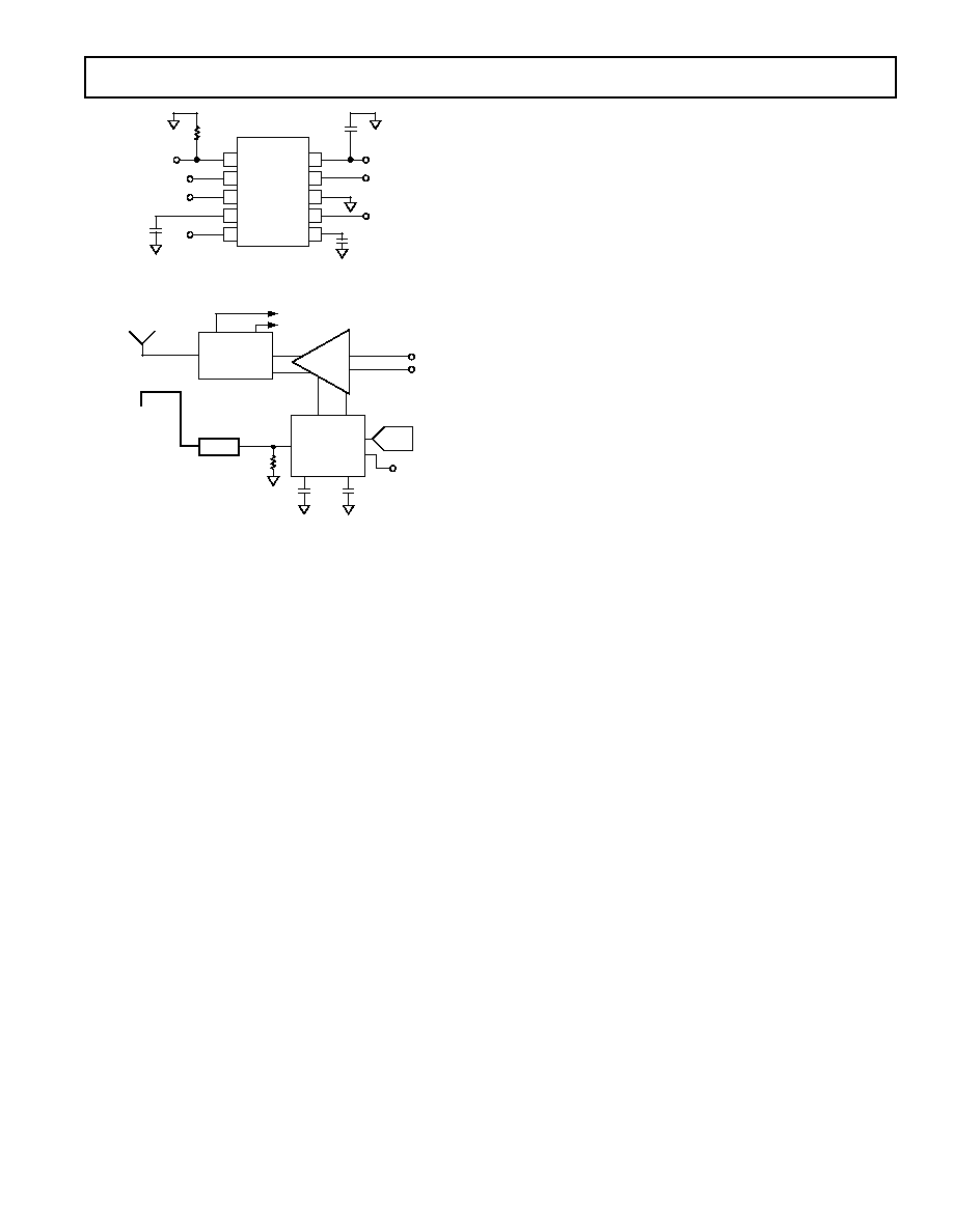
PIN FUNCTION DESCRIPTIONS
Pin No.
MSOP LFCSP
Mnemonic Function
1
1
RFIN
RF Input.
2
2
ENBL
Connect to VPOS for Normal
Operation. Connect pin to
ground for disable mode.
3
3
VSET
Setpoint Input.
4
4
FLT1
Integrator Capacitor for OUT1.
Connect between FLT1 and
COMM.
5
6
BSEL
Band Select. LO = OUT2,
HI = OUT1.
6
7
FLT2
Integrator Capacitor for OUT2.
Connect between FLT2 and
COMM.
7
9
OUT2
Band 2 Output.
8
10, 14
COMM
Device Common (Ground).
9
11
OUT1
Band 1 Output.
10
12
VPOS
Positive Supply Voltage: 2.7 V
to 5.5 V.
5, 8, 13,
NC
No Connection.
15, 16
PIN CONFIGURATION
10-Lead MSOP
AD8316
OUT2
FLT2
VPOS
OUT1
COMM
FLT1
BSEL
RFIN
ENBL
VSET
1
2
3
4
5
10
9
8
7
6
TOP VIEW
(NOT TO SCALE)
16-Lead LFCSP
NC
NC
COMM
NC
VPOS
OUT1
COMM
OUT2
RFIN
ENBL
VSET
FLT1
NC
BSEL
FL
T2
NC
1
2
3
4
12
11
10
9
16
15
14
13
5
6
7
8
AD8316
TOP VIEW
(Not to Scale)
NC = NO CONNECT
Storage Temperature Range . . . . . . . . . . . . . . . ≠65
∞C to +150∞C
Lead Temperature Range (Soldering 60 sec)
MSOP . . . . . . . . . . . . . . . . . . . . . . . . . . . . . . . . . . . . . . . 300
∞C
LFCSP . . . . . . . . . . . . . . . . . . . . . . . . . . . . . . . . . . . . . . 240
∞C
*Stresses above those listed under Absolute Maximum Ratings may cause perma-
nent damage to the device. This is a stress rating only; functional operation of the
device at these or any other conditions above those indicated in the operational
section of this specification is not implied. Exposure to absolute maximum rating
conditions for extended periods may affect device reliability.
CAUTION
ESD (electrostatic discharge) sensitive device. Electrostatic charges as high as 4000 V readily
accumulate on the human body and test equipment and can discharge without detection. Although the
AD8316 features proprietary ESD protection circuitry, permanent damage may occur on devices
subjected to high energy electrostatic discharges. Therefore, proper ESD precautions are recommended
to avoid performance degradation or loss of functionality.
REV. C
≠4≠
AD8316
INPUT AMPLITUDE ≠ dBm
0.6
≠60
V
SET
≠ V
0.4
0.2
≠40
≠30
≠20
0
1.0
≠10
0.8
10
1.6
1.2
1.4
≠50
≠73
≠53
≠43
≠33
≠13
≠23
≠3
≠63
0.9GHz
1.9GHz
2.5GHz
0.1GHz
INPUT AMPLITUDE ≠ dBV
TPC 1. V
SET
vs. Input Amplitude
INPUT AMPLITUDE ≠ dBm
0.6
≠60
V
SET
≠ V
0.4
0
≠40
≠30
≠20
0
1.0
≠10
0.8
10
1.6
1.2
1.4
≠50
≠73
≠53
≠43
≠33
≠13
≠23
≠3
≠63
0.2
≠1
≠2
≠4
1
0
4
2
3
≠3
INPUT AMPLITUDE ≠ dBV
ERROR ≠ dB
≠30 C
+25 C
+85 C
≠30 C
+25 C
+85 C
TPC 2. V
SET
and Log Conformance vs. Input
Amplitude at 0.1 GHz
INPUT AMPLITUDE ≠ dBm
0.6
≠60
V
SET
≠ V
0.4
0
≠40
≠30
≠20
0
1.0
≠10
0.8
10
1.6
1.2
1.4
≠50
≠73
≠53
≠43
≠33
≠13
≠23
≠3
≠63
0.2
≠1
≠2
≠4
1
0
4
2
3
≠3
INPUT AMPLITUDE ≠ dBV
ERROR ≠ dB
≠30 C
+25 C
+85 C
≠30 C
+25 C
+85 C
TPC 3. V
SET
and Log Conformance vs. Input
Amplitude at 0.9 GHz
INPUT AMPLITUDE ≠ dBm
≠1
≠60
≠2
≠4
≠40
≠30
≠20
0
1
≠10
0
10
4
2
3
≠50
≠73
≠53
≠43
≠33
≠13
≠23
≠3
≠63
≠3
INPUT AMPLITUDE ≠ dBV
1.9GHz
1.9GHz
0.9GHz
2.5GHz
ERROR ≠ dB
0.1GHz
TPC 4. Log Conformance vs. Input Amplitude at
Selected Frequencies
INPUT AMPLITUDE ≠ dBm
0.6
≠60
V
SET
≠ V
0.4
0
≠40
≠30
≠20
0
1.0
≠10
0.8
10
1.6
1.2
1.4
≠50
≠73
≠53
≠43
≠33
≠13
≠23
≠3
≠63
0.2
INPUT AMPLITUDE ≠ dBV
ERROR ≠ dB
≠1
≠2
≠4
1
0
4
2
3
≠3
+25 C
≠30 C
+85 C
+25 C
≠30 C
+85 C
TPC 5. V
SET
and Log Conformance vs. Input
Amplitude at 1.9 GHz
INPUT AMPLITUDE ≠ dBm
0.6
≠60
V
SET
≠ V
0.4
0
≠40
≠30
≠20
0
1.0
≠10
0.8
10
1.6
1.2
1.4
≠50
≠73
≠53
≠43
≠33
≠13
≠23
≠3
≠63
0.2
INPUT AMPLITUDE ≠ dBV
ERROR ≠ dB
≠1
≠2
≠4
1
0
4
2
3
≠3
+25 C
≠30 C
+85 C
+25 C
≠30 C
+85 C
TPC 6. V
SET
and Log Conformance vs. Input
Amplitude at 2.5 GHz
≠Typical Performance Characteristics
REV. C
AD8316
≠5≠
INPUT AMPLITUDE ≠ dBm
≠1
≠60
ERROR ≠ dB
≠2
≠4
≠40
≠30
≠20
0
1
≠10
0
10
4
2
3
≠50
≠73
≠53
≠43
≠33
≠13
≠23
≠3
≠63
≠3
INPUT AMPLITUDE ≠ dBV
+85 C
≠30 C
TPC 7. Distribution of Error at Temperature after Ambient
Normalization vs. Input Amplitude, 3 Sigma to Either Side
of Mean, 0.1 GHz
INPUT AMPLITUDE ≠ dBm
≠1
≠60
ERROR ≠ dB
≠2
≠4
≠40
≠30
≠20
0
1
≠10
0
10
4
2
3
≠50
≠73
≠53
≠43
≠33
≠13
≠23
≠3
≠63
≠3
INPUT AMPLITUDE ≠ dBV
+85 C
≠30 C
TPC 8. Distribution of Error at Temperature after Ambient
Normalization vs. Input Amplitude, 3 Sigma to Either Side
of Mean, 0.9 GHz
FREQUENCY ≠ GHz
700
0
RESISTANCE ≠
1000
100
0.5
1.5
2.0
1600
1300
2.5
3100
1900
2500
400
1.0
≠1200
≠1600
≠2000
≠600
≠800
0
≠400
≠200
≠1800
REACTANCE ≠
X
2800
2200
≠1400
≠1000
R (CSP)
FREQ
MSOP
CHIP-SCALE (LFCSP)
(GHz)
0.1
0.9
1.9
2.5
R
≠
3100
≠
600
≠
320
≠
110
≠
jX
j1220
j194
j134
j86
R
≠
2630
≠
1000
≠
620
≠
435
≠
jX
j1800
j270
j130
j110
R
X (LFCSP)
X (MSOP)
R (MSOP)
TPC 9. Input Impedance vs. Frequency
INPUT AMPLITUDE ≠ dBm
≠1
≠60
ERROR ≠ dB
≠2
≠4
≠40
≠30
≠20
0
1
≠10
0
10
4
2
3
≠50
≠73
≠53
≠43
≠33
≠13
≠23
≠3
≠63
≠3
INPUT AMPLITUDE ≠ dBV
+85 C
≠30 C
TPC 10. Distribution of Error at Temperature after Ambient
Normalization vs. Input Amplitude, 3 Sigma to Either Side
of Mean, 1.9 GHz
INPUT AMPLITUDE ≠ dBm
≠1
≠60
ERROR ≠ dB
≠2
≠4
≠40
≠30
≠20
0
1
≠10
0
10
4
2
3
≠50
≠73
≠53
≠43
≠33
≠13
≠23
≠3
≠63
≠3
INPUT AMPLITUDE ≠ dBV
+85 C
≠30 C
TPC 11. Distribution of Error at Temperature after Ambient
Normalization vs. Input Amplitude, 3 Sigma to Either Side
of Mean, 2.5 GHz
V
ENBL
≠ V
0.8
SUPPLY CURRENT ≠ mA
1.0 1.1 1.2
1.4
1.3
1.5
8
0.9
6
4
2
0
1.6 1.7 1.8 1.9 2.0 2.1 2.2 2.3
INCREASING
V
ENBL
DECREASING
V
ENBL
TPC 12. Supply Current vs. V
ENBL
REV. C
≠6≠
AD8316
FREQUENCY ≠ GHz
0
SLOPE ≠ mV/dB
0.5
1.0
23
21
20
1.5
2.0
2.5
+25 C
22
+85 C
≠30 C
TPC 13. Slope vs. Frequency at Selected Temperatures
V
S
≠ V
2.5
SLOPE ≠ mV/dB
3.0
3.5
22.5
21.0
20.5
4.0
4.5
5.0
22.0
0.9GHz
0.1GHz
1.9GHz
2.5GHz
21.5
5.5
TPC 14. Slope vs. Supply Voltage
FREQUENCY ≠ Hz
1
AMPLITUDE ≠ dB
10
100
50
1k
10k
100k
1M
40
30
20
10
0
≠10
≠20
≠30
≠40
≠50
≠60
0
≠20
≠40
≠60
≠80
≠100
≠120
≠140
≠160
≠180
≠200
≠210
PHASE ≠ Degrees
10M
100M
C
FLT
= 0pF
C
FLT
= 220pF
TPC 15. AC Response from VSET to OUT1 and OUT2
FREQUENCY ≠ GHz
0
INTERCEPT ≠ dBm
≠66
≠68
0.5
1.0
2.0
1.5
≠64
≠60
≠62
≠30 C
+25 C
+85 C
2.5
TPC 16. Intercept vs. Frequency at Selected Temperatures
V
S
≠ V
2.5
INTERCEPT ≠ dBm
≠68
≠70
3.0
3.5
5.0
4.5
≠64
≠58
≠60
0.1GHz
5.5
≠62
≠66
4.0
0.9GHz
1.9GHz
2.5GHz
TPC 17. Intercept vs. Supply Voltage
NOISE SPECTRAL DENSITY ≠ nV/
Hz
FREQUENCY ≠ Hz
100
10
1k
10k
10M
1M
10000
1000
100M
100
100k
≠50dBm
≠40dBm
≠25dBm
0dBm
≠20dBm
≠10dBm
RF INPUT
28dBm
TPC 18. Output Noise Spectral Density, R
L
=
,
C
FLT
= 220 pF, by RF Input Amplitude
REV. C
AD8316
≠7≠
V
S
≠ V
2.7
V
OUT
≠ V
1.9
2.8
2.9
3.2
3.1
3.5
2.9
3.3
2.5
3.0
0mA
3.3
3.1
2.7
2.3
2.1
3.4
3.5
2mA
4mA
6mA
8mA
10mA
12 mA
I
LOAD
TPC 19. Maximum OUT Voltage vs. Supply Voltage by
Load Current, AD8316 Sourcing
V
ENBL
GND
V
OUT
GND
C
FLT
= 68pF
AVERAGING = 16 SAMPLES
50mV PER
VERTICAL
DIVISION
C
FLT
= 220pF
1V PER
VERTICAL
DIVISION
2 s PER HORIZONTAL DIVISION
TPC 20. ENBL Response Time, Rise/Fall Time = 250 ns
52.3
2.7V
AD8316
OUT2
FLT2
VPOS
OUT1
COMM
FLT1
BSEL*
RFIN
ENBL
VSET
C
FLT
C
FLT
H-P 8110A
PULSE
GENERATOR
TEK P6204
FET PROBE
R
L
1k
TEK 1103
PWR SUPPLY
TEK TDS3054
SCOPE
0.1 F
RF OUT
H-P 8648B
SIGNAL
GENERATOR
PULSE OUT
TEK P6204
FET PROBE
2.7V
*BSEL HIGH
OUT1;
BSEL LOW
OUT2
0.1GHz
60dBm
TPC 21. Test Setup for ENBL Response Time
V
S
≠ V
2.7
V
OUT
≠ V
2.2
2.9
2.8
2.6
2.8
2.7
2.5
2.4
3.0
6mA
2.3
SHADING INDICATES 3 SIGMA
2mA
TPC 22. Distribution of Maximum OUT Voltage vs. Supply
Voltage with 2 mA and 6 mA Loads, 3 Sigma to Either
Side of Mean, AD8316 Sourcing
GND
AVERAGING = 16 SAMPLES
1V PER
VERTICAL
DIVISION
2 s PER HORIZONTAL DIVISION
GND
BSEL INPUT
V
OUT2
10mV PER VERTICAL DIVISION
TPC 23. BSEL Response Time, ENBL Grounded
RF OUT
H-P 8648B
SIGNAL
GENERATOR
0.1GHz
≠60dBm
52.3
2.7V
AD8316
OUT2
FLT2
VPOS
OUT1
COMM
FLT1
BSEL*
RFIN
ENBL
VSET
C
FLT
H-P 8110A
PULSE
GENERATOR
PULSE OUT
TEK P6204
FET PROBE
C
FLT
TEK P6204
FET PROBE
R
L
1k
TEK 1103
PWR SUPPLY
TEK TDS3054
SCOPE
0.1 F
*BSEL HIGH
OUT1;
BSEL LOW
OUT2
TPC 24. Test Setup for BSEL Response Time
REV. C
≠8≠
AD8316
GND
2V PER
VERTICAL
DIVISION
2 s PER HORIZONTAL DIVISION
GND
50mV PER
VERTICAL
DIVISION
C
FLT
= 220pF
C
FLT
= 68pF
V
OUT
AVERAGING = 16 SAMPLES
V
POS
/V
ENBL
250ns
RISE TIME
TPC 25. Power-On and Power-Off Response with
VSET Grounded, Rise/Fall Time = 250 ns
GND
2V PER
VERTICAL
DIVISION
2 s PER HORIZONTAL DIVISION
GND
50mV PER
VERTICAL
DIVISION
C
FLT
= 68pF
V
OUT
C
FLT
= 220pF
1 s
RISE TIME
AVERAGING = 16 SAMPLES
V
POS
/V
ENBL
TPC 26. Power-On and Power-Off Response with
VSET Grounded, Rise/Fall Time = 1
µs
RF OUT
H-P 8648B
SIGNAL
GENERATOR
0.1GHz
≠60dBm
52.3
AD8316
OUT2
FLT2
VPOS
OUT1
COMM
FLT1
BSEL*
RFIN
ENBL
VSET
C
FLT
C
FLT
H-P 8110A
PULSE
GENERATOR
R
L
1k
TEK 1103
PWR SUPPLY
TEK TDS3054
SCOPE
PULSE OUT
*BSEL HIGH
OUT1;
BSEL LOW
OUT2
AD811
TEK P6204
FET PROBE
732
49.9
TEK P6204
FET PROBE
TPC 27. Test Setup for Power-On and Power-Off
Response with VSET Grounded
GND
PULSED RF
INPUT
0.1GHz, ≠3dBm
100ns PER HORIZONTAL DIVISION
GND
V
OUT
1V PER
VERTICAL
DIVISION
AVERAGING = 16 SAMPLES
TPC 28. Pulse Response Time, Full-Scale Amplitude
Change, Open Loop, C
FLT
= 0 pF
1V PER
VERTICAL
DIVISION
GND
PULSED RF
INPUT
0.1GHz, ≠3dBm
2 s PER HORIZONTAL DIVISION
GND
V
OUT
AVERAGING = 16 SAMPLES
TPC 29. Pulse Response Time, Full-Scale Amplitude
Change, Open Loop, C
FLT
= 68 pF
RFOUT
H-P 8648B
SIGNAL
GENERATOR
0.1GHz
0dBm
52.3
3dB
PWR DIVIDER
PULSE MODE IN
10MHz REF OUT
AD8316
C
FLT
C
FLT
H-P 8110A
PULSE
GENERATOR
PULSE OUT
TRIG OUT
EXT TRIG
TEK P6204
FET PROBE
R
L
1k
TEK 1103
PWR SUPPLY
TEK TDS3054
SCOPE
0.1 F
2.7V
BSEL HIGH
OUT1;
BSEL LOW
OUT2
TEK P6204
FET PROBE
2.7V
2.7V
0.4V
*
OUT2
FLT2
VPOS
OUT1
COMM
FLT1
BSEL*
RFIN
ENBL
VSET
TPC 30. Test Setup for Pulse Response Time
REV. C
AD8316
≠9≠
10mV PER
VERTICAL
DIVISION
2V PER
VERTICAL DIVISION
2 s PER HORIZONTAL DIVISION
V
OUT
AVERAGING = 16 SAMPLES
V
POS
INPUT
250ns
RISE TIME
1 s
RISE TIME
TPC 31. Power-On and Power-Off Response with
VSET and ENBL Grounded
RFOUT
H-P 8648B
SIGNAL
GENERATOR
0.1GHz
≠60dBm
52.3
AD8316
OUT2
FLT2
VPOS
OUT1
COMM
FLT1
BSEL*
RFIN
ENBL
VSET
C
FLT
C
FLT
H-P 8110A
PULSE
GENERATOR
R
L
1k
TEK 1103
PWR SUPPLY
TEK TDS3054
SCOPE
PULSE OUT
*BSEL HIGH
OUT1;
BSEL LOW
OUT2
AD811
TEK P6204
FET PROBE
732
49.9
TEK P6204
FET PROBE
TPC 32. Test Setup for Power-On and Power-Off
Response with VSET and ENBL Grounded
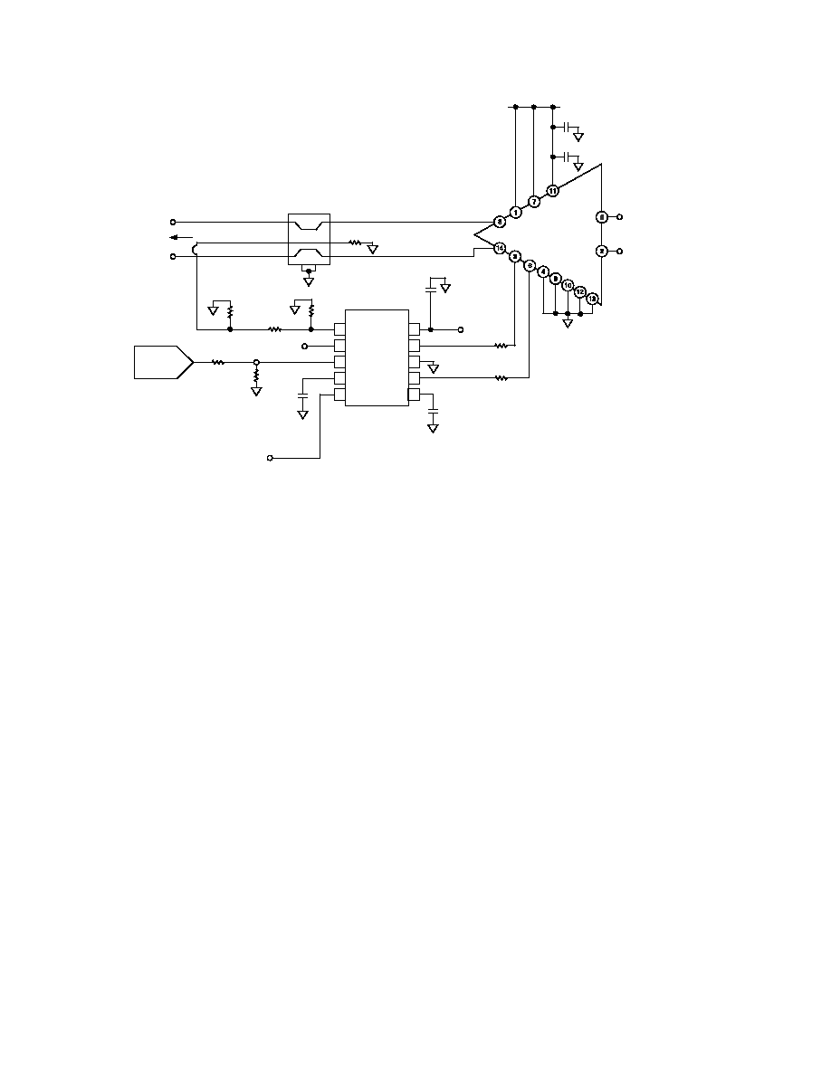
GENERAL DESCRIPTION AND THEORY
The AD8316 is a wideband logarithmic amplifier (log amp) with
two selectable outputs suitable for dual-band/dual-mode power
amplifier control. It is strictly optimized for power control appli-
cations rather than for use as a measurement device. Figure 1
shows its main features in block schematic form. The output
pins, OUT1 and OUT2, are intended to be applied directly to
the automatic power control (APC) pins of two distinct power
amplifiers. When the band select pin, BSEL, directs one of the
controller outputs to servo its amplifier toward the setpoint
indicated by the power control pin VSET, the other output is
forced to ground, disabling the second amplifier. Each output
has a dedicated filter pin, FLT1 and FLT2, that allows the
filtering and loop dynamics for each control loop to be opti-
mized independently.
Basic Theory
Logarithmic amplifiers provide a type of compression in which a
signal with a large range of amplitudes is converted to one of
a smaller range. The use of the logarithmic function uniquely
results in the output representing the decibel value of the input.
The fundamental mathematical form is
V
V
V
V
OUT
SLP
IN
Z
=
log
(1)
Here V
IN
is the input voltage and V
Z
is called the intercept (volt-
age) because when V
IN
= V
Z
the argument of the logarithm is
unity, and thus the result is zero; V
SLP
is called the slope (volt-
age), which is the amount by which the output changes for a
certain change in the ratio (V
IN
/V
Z
).
Because log amps do not respond to power, but only to voltages,
and the calibration of the intercept is waveform dependent and
only quoted for a sine wave signal, the equivalent power response
can be written as
V
V
P
P
OUT
DB
IN
Z
=
(
≠
)
(2)
where the input power P
IN
and the equivalent intercept P
Z
are
both expressed in dBm (thus, the quantity in the parentheses is
simply a number of decibels), and V
DB
is the slope expressed as
so many mV/dB. When base 10 logarithms are used, denoted by
the function log
10
, V
SLP
represents V/dec, and since a decade
corresponds to 20 dB, V
SLP
/20 represents the change in V/dB. For
the AD8316, a nominal (low frequency) slope of 22 mV/dB
(corresponding to a V
SLP
of 0.022 mV/dB
◊ 20 dB = 440 mV)
was chosen, and the intercept V
Z
was placed at the equivalent of
≠74 dBV, or 199
µV rms, for a sine wave input. This corre-
sponds to a power level of ≠61 dBm when the net resistive part
of the input impedance of the log amp is 50
. However, both
the slope and the intercept are dependent on frequency (see for
example, TPC 13 and TPC 16).
For a log amp with a slope V
DB
of +22 mV/dB and an inter-
cept at ≠61 dBm, the output voltage for an input power of
≠30 dBm is 0.022
◊ (≠30 ≠ [≠61]) = 0.682 V.
OUT2
OUT1
FLT1
VSET
325mV TO
1.4V = 49dB
FLT2
10dB
COMM
OFFSET
COMPENSATION
RFIN
10dB
10dB
10dB
DET
DET
DET
DET
DET
INTERCEPT
POSITIONING
LOW NOISE
GAIN BIAS
LOW NOISE
BAND GAP
REFERENCE
OUTPUT
ENABLE
DELAY
ENBL
VPOS
BSEL
1.35
HI-Z
HI-Z
V≠I
LOW NOISE
RAIL-TO-RAIL
BUFFERS
1.35
Figure 1. Block Schematic of the AD8316
REV. C
≠10≠
AD8316
Further details about the structure and function of log amps are
provided in data sheets for other log amps produced by Analog
Devices. The AD640 and AD8307 include detailed discussions
of the basic principles of operation and explain why the intercept
depends on waveform, an important consideration when complex
modulation is imposed on an RF carrier.
The intercept need not correspond to a physically realizable part
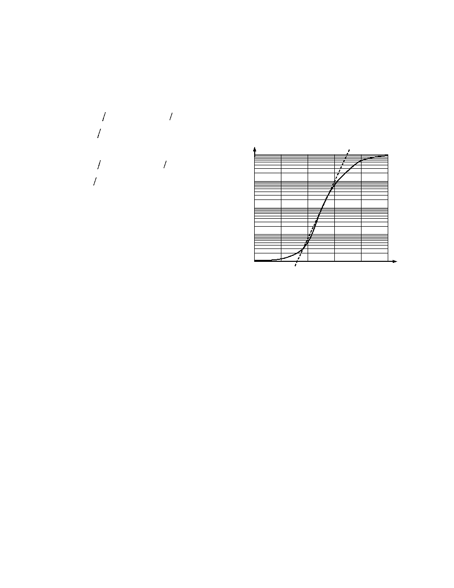
of the signal range for the log amp. Thus, for the AD8316, the
specified intercept is ≠62 dBm at 0.9 GHz, whereas the lowest
acceptable input for accurate measurement (+1 dB error) is
≠48 dBm. At 2.5 GHz, the +1 dB error point shifts to ≠52 dBm.
This positioning of the intercept is deliberate and ensures that
the VSET voltage is within the capabilities of certain DACs,
whose outputs cannot swing below 200 mV. Figure 2 shows the
0.9 GHz response of the AD8316; the vertical axis represents
the value required at the power control pin VSET to null the
control loop rather than the voltage at the OUT1 or OUT2
pins.
P
IN
0.5V
≠67dBm
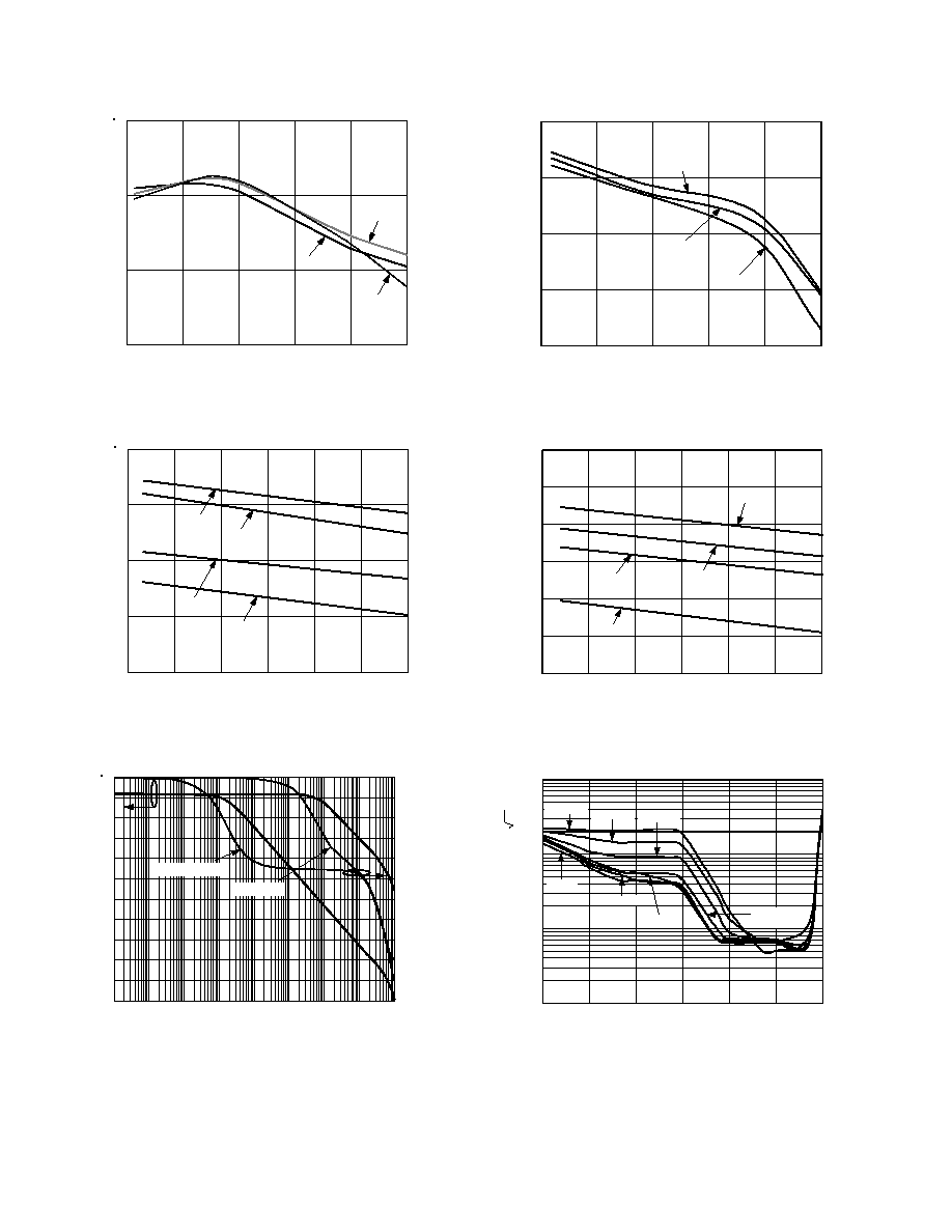
V
SET
0
1.5V
1.0V
100 V
80dBV
V
IN
, dBV
IN
1mV
60dBV
10mV
40dBV
100mV
20dBV
1V (rms)
0dBV
≠47dBm
≠27dBm
≠7dBm
+13dBm
≠62dBm
SLOPE = 22mV/dB
IDEAL
0.308V AT ≠48dBm
ACTUAL
1.408V AT +2dBm
Figure 2. Basic Calibration of the AD8316 at 0.9 GHz
Controller-Mode Log Amps
The AD8316 combines the two key functions required for the
measurement and control of the power level over a moder-
ately wide dynamic range. First, it provides the amplification
needed to respond to small signals with a chain of four ampli-
fier/limiter cells, each with a small signal gain of 10 dB and a
bandwidth of approximately 4 GHz (see Figure 1). At the
output of each of these amplifier stages is a full-wave recti-
fier, essentially a square-law detector cell that converts the
RF signal voltages to a fluctuating current having an average
value that increases with signal level. A passive detector stage is
added ahead of the first stage. These five detectors are separated
by 10 dB, spanning 50 dB of dynamic range. Their outputs are
in the form of a differential current, making summation a
simple matter. It is readily shown that the summed output can
closely approximate a logarithmic function. The overall accu-
racy at the extremes of the total range, viewed as the deviation
from an ideal logarithmic response, that is, the law-conformance
error, can be judged by referring to TPC 4, which shows that
errors across the central 40 dB are moderate. Other perfor-
mance curves show how conformance to an ideal logarithmic
function varies with supply voltage, temperature, and frequency.
In a device intended for measurement applications, this current
would be converted to an equivalent voltage to provide the
log(V
IN
) function shown in Equation 1. However, the design of
the AD8316 differs from standard practice in that its output
needs to be a low noise control voltage for an RF power ampli-
fier, not a direct measure of the input level. Further, it is highly
desirable that this voltage be proportional to the time integral of
the error between the actual input V
IN
and a dc voltage V
SET
(applied to Pin 3, VSET) that defines the setpoint, that is, a
target value for the power level, typically generated by a DAC.
This is achieved by converting the difference between the sum
of the detector outputs (still in current form) and an internally
generated current proportional to VSET to a single-sided
current-mode signal. This, in turn, is converted to a voltage
(at FLT1 or FLT2, the low-pass filter capacitor nodes) to
provide a close approximation to an exact integration of the
error between the power present in the termination at the input
of the AD8316 and the setpoint voltage. Finally, the voltages
developed across the ground referenced filter capacitors C
FLT
are buffered by a special low noise amplifier of low voltage
gain (
◊1.35) and presented at OUT2 or OUT1 for use as the
control voltage for the appropriate RF power amplifier. This
buffer can provide rail-to-rail swings and can drive a substan-
tial load current, including large capacitors. Note: The RF
power delivered by the power amplifier is assumed to increase mono-
tonically with an increasingly positive voltage on its APC control pin.
Band selection in the AD8316 relies on the fact that dual-band/
dual-mode amplifier systems require only one active amplifier at
a time. This allows both amplifier outputs to share the RF input
of the AD8316 (Pin 1, RFIN) as long as the inactive amplifier is
disabled, i.e., it is not delivering RF power. In this case, power
control is directed solely through the selected amplifier. The
AD8316 ensures that the output control pin associated with the
unselected amplifier pulls its APC pin to ground. It is assumed
that the amplifier is essentially disabled when its APC pin is
grounded.
Control Loop Dynamics
To understand how the AD8316 behaves in a complete control
loop, it is necessary to develop an expression for the current in
the integration capacitor as a function of the input V
IN
and the
setpoint voltage V
SET
. Refer to Figure 3.
1.35
C
FLT
4
FLT1
9
VOUT1
V
SET
V
IN
I
DET
SETPOINT
INTERFACE
3
RFIN
1
LOGARITHMIC
RF DETECTION
SUBSYSTEM
I
ERR
VSET
I
SET
= V
SET
/ 4.15k
I
DET
= I
SLP
log
10
(V
IN
/V
Z
)
Figure 3. Behavioral Model for the AD8316 with
OUT1 Selected
First, write the summed detector currents as a function of the
input:
I
I
V
V
DET
SLP
IN
Z
=
log
(
/
)
10
(3)
where I
DET
is the partially filtered demodulated signal, whose
exact average value will be extracted through the subsequent
integration step; I
SLP
is the current-mode slope, and has a value
of 106 mA per decade (that is, 5.3 mA/dB); V
IN
is the input in
REV. C
AD8316
≠11≠
volts rms; and V
Z
is the effective intercept voltage, which, as
previously noted, is dependent on waveform but is 199
µV rms
for a sine wave input. Now, the current generated by the setpoint
interface is simply
I
V
k
SET
SET
=
/ .
4 15
(4)
I
ERR
, the difference between this current and I
DET
, is applied to
the loop filter capacitor C
FLT
. It follows that the voltage appearing
on this capacitor, V
FLT
, is the time integral of the difference
current
V
s
I
I
sC
FLT
SET
DET
FLT
( )
(
≠
) /
=
(5)
=
V
k
I
V
V
sC
SET
SLP
IN
Z
FLT
/ .
≠
log (
/ )
4 15
10
(6)
The control output V
OUT
is slightly greater than this, since the
gain of the output buffer is
◊1.35. Also, an offset voltage is delib-
erately introduced in this stage, but this is inconsequential, since
the integration function implicitly allows for an arbitrary constant
to be added to the form of Equation 6. The polarity is such that
V
OUT
will rise to its maximum value for any value of V
SET
greater
than the equivalent value of V
IN
. In practice, the output will rail
to the positive supply under this condition unless the control
loop through the power amplifier is present. In other words, the
AD8316 seeks to drive the RF power to its maximum value when-
ever it falls below the setpoint. The use of exact integration results
in a final error that is theoretically zero, and the logarithmic
detection law would ideally result in a constant response time
following a step change of either the setpoint or the power level, if
the power amplifier control function were likewise "linear-in-dB."
This latter condition is rarely true, however, and it follows that
the loop response time will, in practice, depend on the power level,
and this effect can strongly influence the design of the control loop.
Equation 6 can be clarified by noting that it can be restated in
the following way
V
s
V
V
V
V
sT
OUT
SET
SLP
IN
Z
( )
≠
log (
/
)
=
10
(7)
where V
SLP
is the volts-per-decade slope from Equation 1, having a
value of 440 mV/dec, and T is an effective time constant for
the integration, being equal to (4.15 k
◊ C
FLT
)/1.35; the resis-
tor value comes from the setpoint interface scaling Equation 4
and the factor 1.35 arises as a result of the voltage gain of the
buffer. So the integration time constant can be written as
T
C
in s when C
is
ressed in nF
FLT
FLT
=
◊
(
)
3 07
.
µ
exp
(8)
To simplify understanding of the control loop dynamics, begin
by assuming that the power amplifier gain function actually is
linear-in-dB; for now, we will also use voltages to express the
signals at the power amplifier input and output. Let the RF output
voltage be V
PA
and its input be V
CW
; further, to characterize the
gain control function, this form is used
V
G V
PA
O
CW
=
10
(
/
)
V
V
OUT
GSC
(9)
where G
O
is the gain of the power amplifier when V
OUT
= 0 and
V
GSC
is the gain scaling. While few amplifiers will conform so
conveniently to this law, it nevertheless provides a clearer starting
point for understanding the more complex situation that arises
when the gain control law is less than ideal.
This idealized control loop is shown in Figure 4. With some
manipulation, it is found that the characteristic equation of this
system is
V
s
V
V
V
V
kG V
V
sT
OUT
SET
GSC
SLP
GSC
O
CW
Z
O
( )
(
)/
log
(
/
)
=
-
+
10
1
(10)
where k is the voltage coupling factor from the output of the
power amplifier to the input of the AD8316 (e.g.,
◊0.1 for a 20 dB
coupler) and T
O
is a modified time constant (V
GSC
/V
SLP
)T.
This is quite easy to interpret. First, it shows that a system of
this sort will exhibit a simple single-pole response, for any power
level, with the customary exponential time domain form for
either increasing or decreasing step polarities in the demand
level V
SET
or the carrier input V
CW
. Second, it reveals that the
final value of the control voltage V
OUT
will be determined by
several fixed factors
V
t
V
V
V
V
kG V
V
OUT
SET
GSC
SLP
GSC
O
CW
Z
=
(
)
=
-
(
)/
log
(
/
)
10
(11)
RF PA
V
CW
RF DRIVE: UP
TO 2.5GHz
V
RF
DIRECTIONAL COUPLER
C
FLT
AD8316
RESPONSE-SHAPING
OF OVERALL CONTROL
LOOP (EXTERNAL CAP)
V
SET
V
IN
= kV
RF
V
OUT1
Figure 4. Idealized Control Loop for Dynamic
Analysis, OUT1 Selected
Example
Assume that the gain magnitude of the power amplifier runs from
a minimum value of
◊0.316 (≠10 dB) at V
OUT
= 0 to
◊100
(40 dB) at V
OUT
= 2.5 V. Applying Equation 9, we find G
O
=
0.316 and V
GSC
= 1 V. Using a coupling factor of k = 0.0316
(that is, a 30 dB directional coupler) and recalling that the nominal
value of V
SLP
is 440 mV and V
Z
= 199
µV for the AD8316, we will
first calculate the range of values needed for V
SET
to control an
output range of +32 dBm to ≠17 dBm. Note that, in the steady
state, the numerator of Equation 7 must be zero, that is
V
V
kV
V
SET
SLP
PA
Z
=
(
)
log
10
(12)
when V
IN
is expanded to kV
PA
, the fractional voltage sample of
the power amplifier output. Now, for +32 dBm, V
PA
= 8.9 V rms,
this evaluates to
V
max
mV/
V
V
SET
( )
=
(
)
=
0 44
281
199
1 39
10
.
log
.
µ
(13)
For a delivered power of ≠17 dBm, V
PA
= 31.6 mV rms,
V
min
. mV/
V
V
SET
( )
=
(
)
=
0 44
1 0
199
0 310
10
.
log
.
µ
(14)
Note: The power range is 49 dB, which corresponds to a voltage
change of 49 dB
◊ 22 mV/dB = 1.08 V in V
SET
.
REV. C
≠12≠
AD8316
The value of V
OUT
is of interest, although it is a dependent param-
eter inside the loop. It depends on the characteristics of the
power amplifier, and the value of the carrier amplitude V
CW
.
Using the control values derived above, that is, G
O
= 0.316 and
V
GSC
= 1 V, and assuming that the applied power is fixed at
≠7 dBm (so that V
CW
= 100 mV rms), Equation 11 shows
V
max
V
V
V
kG V
V
V
V
OUT
SET
GSC
SLP
O
CW
Z
( )
=
(
)
-
(
)
=
◊
(
)
-
◊
◊
=
-
=
log
.
.
log
.
.
. /
.
.
.
10
10
1 39
1 0 44
0 0316
0 316
0 1 199
3 2
0 7
2 5
µ
(15)
V
min
V
V
V
kG V
V
V
OUT
SET
GSC
SLP
O
CW
Z
( )
=
(
)
-
(
)
=
◊
(
)
-
◊
◊
=
-
=
log
.
.
log
.
.
. /
.
.
10
10
0 31 1 0 44
0 0316
0 316
0 1 199
0 7
0 7
0
µ
(16)
Both results are consistent with the assumptions made about the
amplifier control function. Note that the second term is inde-
pendent of the delivered power and is a fixed function of the
drive power.
Finally, the loop time constant for these parameters, using an
illustrative value of 2 nF for the filter capacitor C
FLT
, evaluates to
T
V
V
T
s
nF
s
O
GSC
SLP
=
(
)
=
(
)
◊
◊
( )
=
/
/ .
.
.
1 0 44
3 07
2
13 95
µ
µ
(17)
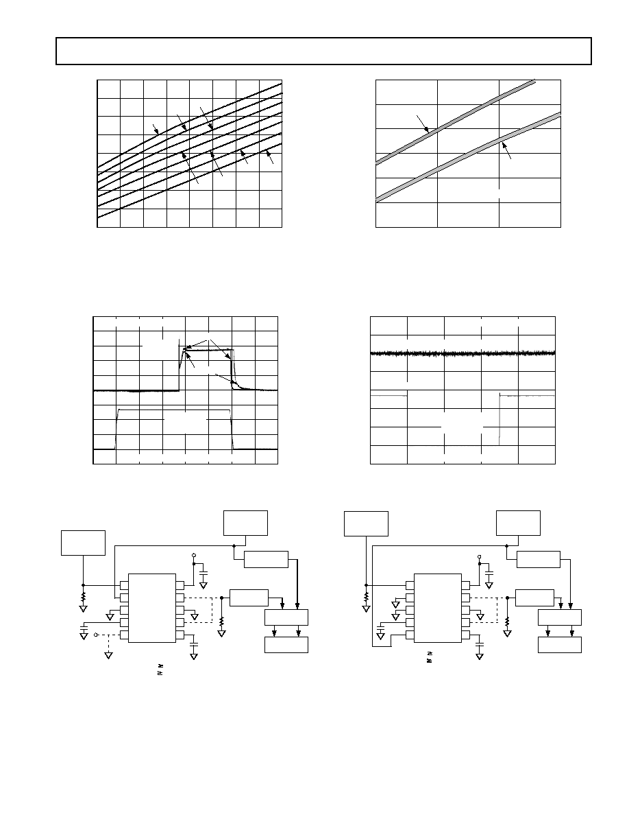
Practical Loop
At the present time, power amplifiers, or VGAs preceding such
amplifiers, do not provide an exponential gain characteristic. It
follows that the loop dynamics (the effective time constant) will
vary with the setpoint, since the exponential function is unique
in providing constant dynamics. The procedure must therefore
be as follows. Beginning with the curve usually provided for the
power output versus APC voltage, draw a tangent at the point
on this curve where the slope is highest (see Figure 5). Using
this line, calculate the effective minimum value of the variable
V
GSC
, and use it in Equation 17 to determine the time constant.
(Note that the minimum in V
GSC
corresponds to the maximum
rate of change in the output power versus V
OUT
.)
For example, suppose it is found that, for a given drive power,
the amplifier generates an output power of P
1
at V
OUT
= V
1
, and
P
2
at V
OUT
= V
2
. Then, it is readily shown that
V
V
V
P
P
GSC
=
(
) (
)
20
2
1
2
1
≠
/
≠
(18)
This should be used to calculate the filter capacitance. The
response time at high and low power levels (on the "shoulders"
of the curve shown in Figure 5) will be slower. Note also that it
is sometimes useful to add a zero in the closed-loop response by
placing a resistor in series with C
FLT
.
A Note About Power Equivalency
Users of the AD8316 must understand that log amps funda-
mentally do not respond to power. For this reason, dBV
(decibels above 1 V rms) are included in addition to the com-
monly used metric dBm. The dBV scaling is fixed, independent
of termination impedance, while the corresponding power level
is not. For example, 224 mV rms is always ≠13 dBV, with one
further condition of an assumed sinusoidal waveform; see the
AD640 data sheet for more information about the effect of wave-
form on logarithmic intercept. This corresponds to a power
of 0 dBm when the net impedance at the input is 50
. When
this impedance is altered to 200
, however, the same voltage
corresponds to a power level that is four times smaller (P = V
2
/R),
or ≠6 dBm. A dBV level may be converted to dBm in the special
case of a 50
system and a sinusoidal signal simply by adding
13 dB. 0 dBV is then, and only then, equivalent to 13 dBm.
≠67dBm
≠47dBm
≠27dBm
≠7dBm
+13dBm
33dBm
23dBm
13dBm
3dBm
≠7dBm
P
RF
V
OUT1
V
2,
P
2
V
1,
P
1
Figure 5. Typical Power Control Curve
Therefore, the external termination added ahead of the AD8316
determines the effective power scaling. This often takes the
form of a simple resistor (52.3
will provide a net 50 input),
but more elaborate matching networks may be used. The choice
of impedance determines the logarithmic intercept, that is, the
input power for which the V
SET
versus P
IN
function would cross
the baseline if that relationship were continuous for all values of
V
IN
. This is never the case for a practical log amp; the intercept
(so many dBV) refers to the value obtained by the minimum-error
straight-line fit to the actual graph of V
SET
versus P
IN
(more
generally, V
IN
). Where the modulation is complex, as in CDMA,
the calibration of the power response needs to be adjusted; the
intercept will remain stable for any given arbitrary waveform.
When a true power (waveform independent) response is needed,
a mean-responding detector, such as the AD8361, should be
considered.
The logarithmic slope, V
SLP
in Equation 1, which is the amount by
which the setpoint voltage needs to be changed for each decade
of input change (voltage or power) is, in principle, independent
of waveform or termination impedance. In practice, it usually
falls off somewhat at higher frequencies, because of the declining
gain of the amplifier stages and other effects in the detector
cells (see TPC 13).
Basic Connections
Figure 6 shows the basic connections for operating the AD8316
and Figure 7 shows a block diagram of a typical application.
The AD8316 is typically used in the RF power control loop of
dual mode and trimode mobile handsets where there is more
than one RF power control line.
REV. C
AD8316
≠13≠
AD8316
OUT2
FLT2
VPOS
OUT1
COMM
FLT1
BSEL
RFIN
ENBL
VSET
1
2
3
4
5
10
9
8
7
6
RFIN
+V
S
V
SET
C
FLT1
V
BSEL
V
OUT1
V
OUT2
C
FLT2
R1
52.3
C1
0.1 F
+V
S
2.7 TO 5.5V
Figure 6. Basic Connections (Shown with MSOP Pinout)
OUT1
DIRECTIONAL
COUPLER
OUT2
FLT2
VSET
FLT1
RFIN
R1
52.3
C
FLT1
C
FLT2
ATTN
DAC
GAIN
CONTROL
VOLTAGES
RFIN1
BSEL
BAND
SELECT
RFIN2
RX1
RX2
TX1
TX2
ANT
PWR
AMP
Figure 7. Block Diagram of Typical Application
A supply voltage of 2.7 V to 5.5 V is required for the AD8316.
The supply to the VPOS pin should be decoupled with a low
inductance 0.1
µF surface-mount ceramic capacitor close to the
device. The AD8316 has an internal input coupling capacitor,
which negates the need for external ac coupling. This capacitor,
along with the device's low frequency input impedance of approxi-
mately 3.0 k
, sets the minimum usable input frequency to around
20 MHz. A broadband 50
input match is achieved in this
example by connecting a 52.3
resistor between RFIN and
ground (COMM). A plot of input impedance versus frequency
is shown TPC 9. Other matching methods are also possible
(see the Input Coupling Options section).
In a power control loop, the AD8316 provides both the detector
and controller functions.
A number of options exist for coupling the RF signal from the
power amplifiers (PA) to the AD8316 input. Because only one
PA output is active at any time, a single RF input on the
AD8316 is sufficient in all cases.
Two directional couplers can be used directly at the PA outputs.
The outputs of these couplers would be passively combined
before being applied to the AD8316 RF input (in general,
some additional attenuation will be required between the coupler
and the AD8316). Another option involves using a dual-direc-
tional coupler between the PA and T/R switch. This device has
two inputs/outputs and a single-coupled output so that no exter-
nal combiner is required.
A third option is to use a single broadband directional coupler
at the output of the transmit/receive (T/R) switch (the outputs
from the two PAs are combined in the T/R switch). This is
shown in Figure 7. This provides the advantage of enabling the
power at the output of the T/R switch to be precisely set, elimi-
nating any errors due to insertion loss and insertion loss
variations of the T/R switch.
A setpoint voltage is applied to VSET from the controlling
source, generally a DAC. Any imbalance between the RF input
level and the level corresponding to the setpoint voltage will be
corrected by the selected output, OUT1 or OUT2, which drives
the gain control terminal of the PAs. This restores a balance
between the actual power level sensed at the input of the AD8316
and the demanded value determined by the setpoint. This assumes
that the gain control sense of the variable gain element is posi-
tive; that is, an increasing voltage from OUT1 or OUT2 will
tend to increase gain. The outputs can swing from 100 mV
above ground to within 100 mV of the supply rail and can source
up to 12 mA. (A plot of maximum output voltage versus output
current is shown in TPC 19.) OUT1/OUT2 are capable of
sinking more than 200
µA.
Range on VSET and RF Input
The relationship between RF input level and the setpoint volt-
age follows from the nominal transfer function of the device (see
TPCs 2, 3, 5, and 6). At 0.9 GHz, for example, a voltage of 1 V
on VSET indicates a demand for ≠17 dBm (≠30 dBV) at RFIN.
The corresponding power level at the output of the power ampli-
fier will be greater than this amount due to the attenuation
through the directional coupler. For setpoint voltages of less
than approximately 200 mV and RF input amplitudes greater
than approximately ≠50 dBm, V
OUT
will remain unconditionally
at its minimum level of approximately 250 mV. This feature can
be used to prevent any spurious emissions during power-up and
power-down phases. Above 250 mV, VSET will have a linear
control range up to 1.4 V, corresponding to a dynamic range of
49 dB. This results in a slope of 22.2 mV/dB or approximately
45.5 dB/V.
Transient Response
The time domain response of power amplifier control loops,
using any kind of controller, is only partially determined by the
choice of filter which, in the case of the AD8316, has a true
integrator form 1/sT, as shown in Equation 7, with a time con-
stant given by Equation 8. The large signal step response is also
strongly dependent on the form of the gain control law. Never-
theless, some simple rules can be applied. When the filter capacitor
C
FLT
is very large, it will dominate the time domain response,
but the incremental bandwidth of this loop will still vary as
V
OUT
traverses the nonlinear gain control function of the PA, as
shown in Figure 5. This bandwidth will be highest at the
point where the slope of the tangent drawn on this curve is
greatest--that is, for power outputs near the center of the PA's
range--and will be much reduced at both the minimum and the
maximum power levels, where the slope of the gain control
curve is lowest, due to its S-shaped form. Using smaller values
of C
FLT
, the loop bandwidth will generally increase, in inverse
proportion to its value. Eventually, however, a secondary effect
will appear, due to the inherent phase lag in the power amplifier's
control path, some of which may be due to parasitic or deliber-
ately added capacitance at the OUT1 and OUT2 pins. This results
in the characteristic poles in the ac loop equation moving off the
real axis and thus becoming complex (and somewhat resonant).
This is a classic aspect of control loop design.
The lowest permissible value of C
FLT
needs to be determined
experimentally for a particular amplifier and circuit board lay-
out. For GSM and DCS power amplifiers, C
FLT
will typically
range from 150 pF to 300 pF.
In many cases, some improvement in the worst-case response
time can be achieved by including a small resistance in series with
C
FLT
; this generates an additional zero in the closed-loop trans-
fer function, which will serve to cancel some of the higher-order
REV. C
≠14≠
AD8316
poles in the overall loop. A combination of main capacitor C
FLT
shunted by a second capacitor and resistor in series will also be
useful in minimizing the settling time of the loop.
Mobile Handset Power Control Example
Figure 8 shows a complete power amplifier control circuit for a
dual-mode handset. The RF3108 (RF Micro Devices), dual-
input, trimode (GSM, DCS, PCS) PA is driven by a nominal
power level of 6 dBm at both inputs and has two gain control
lines. Some of the output power from the PA is coupled off
using a dual-band directional coupler (Murata part number
LDC15D190A0007A). This has a coupling factor of approxi-
mately 20 dB for the GSM band and 15 dB for DCS and an
insertion loss of 0.38 dB and 0.45 dB, respectively. Because the
RF3108 transmits a maximum power level of approximately
35 dBm for GSM and 32 dBm for DCS/PCS, additional attenua-
tion of 20 dB is required before the coupled signal is applied to
the AD8316. This results in peak input levels of ≠5 dBm (GSM)
and ≠3 dBm (DCS). While the AD8316 gives a linear response
for input levels up to +3 dBm, for highly temperature-stable
performance at maximum PA output power, the maximum
input level should be limited to approximately ≠3 dBm (see
TPC 3 and TPC 5). This does, however, reduce the sensitivity
of the circuit at the low end.
The operational setpoint voltage, in the range 250 mV to 1.4 V,
is applied to the VSET pin of the AD8316. This will typically be
supplied by a DAC. The desired output is selected by applying
a high or low signal to the BSEL pin (HI = OUT1, LO = OUT2).
The selected output directly drives the level control pin of the
power amplifier. In this case a minimum supply voltage of 2.9 V
is required and V
OUT
reaches a maximum value of approximately
2.6 V while delivering about 5 mA to the PA's V
APC
input. For
power amplifiers with lower V
APC
input ranges, a corresponding
low power supply to the AD8316 can be used. For example, on
a 2.7 V supply, the voltage on OUT1/OUT2 can come to within
approximately 100 mV of the supply rail. This will depend, how-
ever, on the current draw (see TPC 19).
During initialization and completion of the transmit sequence,
V
OUT
should be held at its minimum level of 250 mV by keeping
V
SET
below 200 mV. In this example, V
SET
is supplied by an 8-bit
DAC that has an output range from 0 V to 2.55 V or 10 mV
per bit. This sets the control resolution of V
SET
to 0.4 dB/bit
(0.04 dB/mV 10 mV). If finer resolution is required, the
DAC's output voltage can be scaled using two resistors as
shown. This converts the DAC's maximum voltage of 2.55 V
down to 1.6 V and increases the control resolution to 0.25 dB/bit.
Two filter capacitors (C
FLT1
/C
FLT2
) must be used to stabilize
the loop for each band. The choice of C
FLT
will depend to a
large degree on the gain control dynamics of the power ampli-
fier, something that is frequently poorly characterized, so some
trial and error may be necessary. In this example, a 220 pF
capacitor is used. The user may want to add a resistor in series
with the filter capacitor. The resistor adds a zero to the control
loop and increases the phase margin, which helps to make the
step response of the circuit more stable when the slope of the
PA's power control function is the steepest. In this example,
the two filter capacitors are equal values; however, this is not
a requirement.
A smaller filter capacitor can be used by inserting a series resis-
tor between V
OUT
and the control input of the PA. A series
resistor will work with the input impedance of the PA to create a
resistor divider and will reduce the loop gain. The size of the
resistor divider ratio depends upon the available output swing of
V
OUT
and the required control voltage on the PA. This tech-
nique can also be used to limit the control voltage in situations
where the PA cannot deliver the power level demanded by V
OUT
. Over-
drive of the control input of some PAs causes increased distortion.
RF3108
4.7 F
1 F
3.5V
GSM RF IN
+6dBm
DCS/PCS RF IN
+6dBm
GND
R6
(R5, R6 OPTIONAL)
(SEE TEXT)
8-BIT
RAMP DAC
0V 2.55V
R2
600
R3
1k
ENABLE
0V/+V
S
R4
576
AD8316
OUT2
VPOS
OUT1
COMM
FLT1
RFIN
ENBL
VSET
1
2
3
4
10
9
8
7
FLT2
BSEL
5
6
C
FLT2
220pF
+V
S
2.7V TO 5.5V
C1
0.1 F
R5
54.9
R1
52.3
GSM/DCS
16.5dBm/19dBm
C
FLT1
220pF
BAND SELECT
0V/+V
S
GSM/(DCS/PCS)
(R2, R3 OPTIONAL)
(SEE TEXT)
5
2
6
3
4
8
LDC15D190A0007A
R7
49.9
7
1
GSM
RF OUTPUT
+35.5dBm MAX
TO
T/R SWITCH
21.5dB ATTENUATOR
PCS/DCS
RF OUTPUT
+33dBm MAX
R8
GSM V
APC
DCS/PCS V
APC
Figure 8. Dual-Mode (GSM/DCS) PA Control Example (Shown with AD8316 MSOP Pinout)

REV. C
AD8316
≠15≠
Enable and Power-On
The AD8316 may be disabled by pulling the ENBL pin to
ground. This reduces the supply current from its nominal level
of 8.5 mA to 3
µA at 2.7 V. The logic threshold for turning on
the device is at 1.8 V at 2.7 V. A plot of the enable glitch is
shown in TPC 20. Alternatively, the device can be completely
disabled by pulling the supply voltage to ground; ENBL would be
connected to VPOS. The glitch in this mode of operation is
shown on TPC 25 and TPC 26. If VPOS is applied before the
device is enabled, a narrow glitch of less than 50 mV will result.
This is shown in TPC 31.
In both situations, the voltage on V
SET
should be kept below
250 mV during power-on and power-off, preventing any unwanted
transients on V
OUT
.
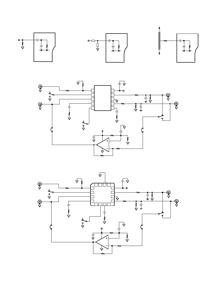
Input Coupling Options
The internal 5 pF coupling capacitor of the AD8316, along with
the low frequency input impedance of 3 k
, result in a high-pass
input corner frequency of approximately 20 MHz. This sets the
minimum operating frequency. Figure 9 shows three options for
input coupling. A broadband resistive match can be implemented
by connecting a shunt resistor to ground at RFIN. This 52.3
resistor (other values can also be used to select different overall
input impedances) combines with the input impedance of the
AD8316 (3 k
1 pF) to give a broadband input impedance of
50
. While the input resistance and capacitance (C
IN
and R
IN
)
will vary by approximately
± 20% from device to device, the
dominance of the external shunt resistor means that the varia-
tion in the overall input impedance will be close to the tolerance
of the external resistor. This method of matching is most useful
in wideband applications or in multimode systems where there
is more than one operating frequency and those frequencies are
quite far apart.
A reactive match can also be implemented as shown in Figure 9b.
This is not recommended at low frequencies because device
tolerances will vary the quality of the match dramatically because
of the large input resistance. For low frequencies, Option 9a or
Option 9c is recommended.
In Figure 9b, the matching components are drawn as generic
reactances. Depending on the frequency, the input impedance
at that frequency, and the availability of standard value compo-
nents, either a capacitor or an inductor will be used. As in the
previous case, the input impedance at a particular frequency is
plotted on a Smith chart and matching components are chosen
(shunt or Series L, shunt or Series C) to move the impedance to
the center of the chart.
Figure 9c shows a third method for coupling the input signal
into the AD8316, applicable where the input signal is larger
than the input range of the log amp. A series resistor, connected
to the RF source, combines with the input impedance of the
AD8316 to resistively divide the input signal being applied to
the input. This has the advantage of very little power being
tapped off in RF power transmission applications.
Using the Chip Scale Package
On the underside of the chip scale package, there is an exposed
paddle. This paddle is internally connected to the chip's ground.
For better electrical performance, this paddle should be soldered
down to the printed circuit board's ground plane, even though
there is no thermal requirement to do so.
EVALUATION BOARD
Figures 10 and 11 show the schematics of the AD8316 MSOP and
LFCSP evaluation boards. Note that uninstalled components are
marked as open. The layout and silkscreen of the MSOP evalua-
tion board are shown in Figures 12 and 13. Apart from the slightly
smaller device footprint and number of pins, the LFCSP evalua-
tion board is identical to the MSOP board. The boards are
powered by a single supply in the 2.7 V to 5.5 V range. The power
supply is decoupled by a single 0.1
µF capacitor. Table II details
the various configuration options of the evaluation boards.
For operation in controller mode, both jumpers, LK1 and LK2,
should be removed. OUT1 and OUT2 can be selected with SW3
in Position A and Position B, respectively. The setpoint voltage
is applied to VSET, RFIN is connected to the RF source (PA
output or directional coupler), and OUT1 or OUT2 is connected
to the gain control pins of each PA. When the AD8316 is used
in controller mode, a capacitor and a resistor must be installed
in C4, C6, and R10, R11 for loop stability. For GSM/DCS
handset power amplifiers, this capacitor should typically range
from 150 pF to 300 pF. The series resistor improves the system
phase margin at low power levels, which in turn improves the
step response in the circuit. Typically, this resistor value should
be about 1.5 k
.
A quasi-measurement mode (in which the AD8316 delivers an
output voltage that is proportional to the log of the input signal)
can be implemented to establish the relationship between V
SET
and RF
IN
with the installation of two jumpers, LK1 and LK2.
This mimics an AGC loop. To establish the transfer function of
the log amp, the RF input should be swept while the voltage on
VSET is measured, that is, the SMA connector labeled VSET
acts as an output. This is the simplest method for validating
operation of the evaluation board. When operated in this
mode, a large capacitor (0.01
µF or greater) must be installed in
C4 or C6 (set R10/R11 to 0
) to ensure loop stability.
REV. C
≠16≠
AD8316
AD8316
OUT2
FLT2
VPOS
OUT1
COMM
FLT1
BSEL
RFIN
ENBL
VSET
1
2
3
4
5
10
9
8
7
6
VPOS
AD8031
R5
10k
R6
17.8k
C3
0.1 F
R8
10k
R7
16.2k
C5
0.1 F
R2
52.3
R1
0
VPOS
B
SW1
J3
VSET
LK1
C4
(OPEN)
R10
(OPEN)
OUT1(A)
OUT2(B)
VPOS
C1
0.1 F
R3
0
J2
OUT1
C2
(OPEN)
R4
(OPEN)
R12
0
R9
(OPEN)
C7
(OPEN)
J4
OUT2
OUT1 (A)
OUT2 (B)
LK2
VPOS
C6
(OPEN)
R11
(OPEN)
SW2
SW3
A
J1
INPUT
Figure 10. Schematic of Evaluation Board (MSOP)
J1
J3
VPOS
SW1
A
B
INPUT
VSET
LK1
R1
0
C4
(OPEN)
R10
(OPEN)
OUT1 (A)
OUT2 (B)
VPOS
SW2
C5
0.1 F
VPOS
R2
52.3
C6
(OPEN)
R11
(OPEN)
C1
0.1 F
VPOS
R12
0
C2
(OPEN)
R4
(OPEN)
R3
0
R9
(OPEN)
C7
(OPEN)
R7
16.2k
C3
0.1 F
OUT1 (A)
OUT2 (B)
SW3
LK2
R8
10k
R6
17.8k
R5
10k
AD8031
J2
OUT1
J4
OUT2
AD8316
RFIN
ENBL
VSET
FLT1
BSEL
FL
T2
COMM
OUT1
VPOS
OUT2
COMM
NC NC
NC
NC
NC
NC = NO CONNECT
1
2
3
4
12
11
10
9
5
6
7
8
13
14
15
16
Figure 11. Schematic of Evaluation Board (LFCSP)
R
IN
C
IN
C
C
AD8316
R
SHUNT
52.3
RFIN
a. Broadband Resistive
R
IN
X2
C
IN
C
C
AD8316
RFIN
X1
b. Narrow-Band Reactive
R
IN
C
IN
C
C
AD8316
RFIN
R
ATTN
STRIPLINE
ANTENNA
PA
c. Series Attenuation
Figure 9. Input Coupling Options

REV. C
AD8316
≠17≠
Table II. Evaluation Board Configuration Options
Component
Function
Default Condition
TP1, TP2
Supply and Ground Vector Pins.
Not Applicable
SW1
Device Enable. When in Position A, the ENBL pin is connected to VPOS and
SW1 = A
the AD8316 is in operating mode. In Position B, the ENBL pin is grounded,
putting the device into power-down mode.
SW2
Band Select. When in Position A (OUT1), the BSEL pin is connected to VPOS
SW2 = OUT1
and the AD8316 OUT1 is in operation mode. In Position B (OUT2), the
BSEL pin is grounded and the AD8316 OUT2 is in operation while OUT1 pin
is shut down.
R1, R2
Input Interface. The 52.3
resistor in Position R2 combines with the AD8316's
R2 = 52.3
(Size 0603)
internal input impedance to provide a broadband input impedance of around
R1 = 0
(Size 0402)
50
. A reactive match can be implemented by replacing R2 with an inductor
and R1 (0
) with a capacitor. In addition, the RF microstrip line has been
provided with a clean mask ground plane to provide additional matching. Note
that the AD8316's RF input is internally ac-coupled.
R3, R4, R12,
Output Interface. R4 and C2, R9 and C7 can be used to check the response
R4 = C2 = Open (Size 0603)
R9, C2, C7
capacitive and resistive loading, respectively. R3/R4 and R12/R9 can be used to
R9 = C7 = Open (Size 0603)
reduce the slope of OUT1 and OUT2.
R3 = R12 = 0
(Size 0603)
C1, C5
Power Supply Decoupling. The nominal supply decoupling consists of
C1 = C5 = 0.1
µF (Size 0603)
a 0.1
µF capacitor.
C4, C6, R10,
Filter Capacitors/Resistors. The response time of OUT1, OUT2 can be modified
C4 = C6 = Open (Size 0603)
R11
by placing the capacitors between FLT1, FLT2 and resistors R10, R11
R10 = R11 = Open (Size 0603)
to ground.
LK1, LK2
Measurement Mode. A quasi-measurement mode can be implemented by
LK1, LK2 = Installed
installing LK1 and LK2 (connecting an inverted OUT1 or OUT2 to VSET) to
yield the nominal relationship between RFIN and VSET. In this mode, a large
capacitor (0.01
µF or greater) must be installed in C4 and C6 and a 0
resistors to ground in R10 and R11. To select OUT1 or OUT2, SW3 must
be in the OUT1 position or the OUT2 position, respectively.
SW3
Measurement Mode Output Select. When in measurement mode, output 1
SW3 = OUT1
or output 2 can be selected by positioning SW3 to the OUT1 position or the
OUT2 position, respectively.
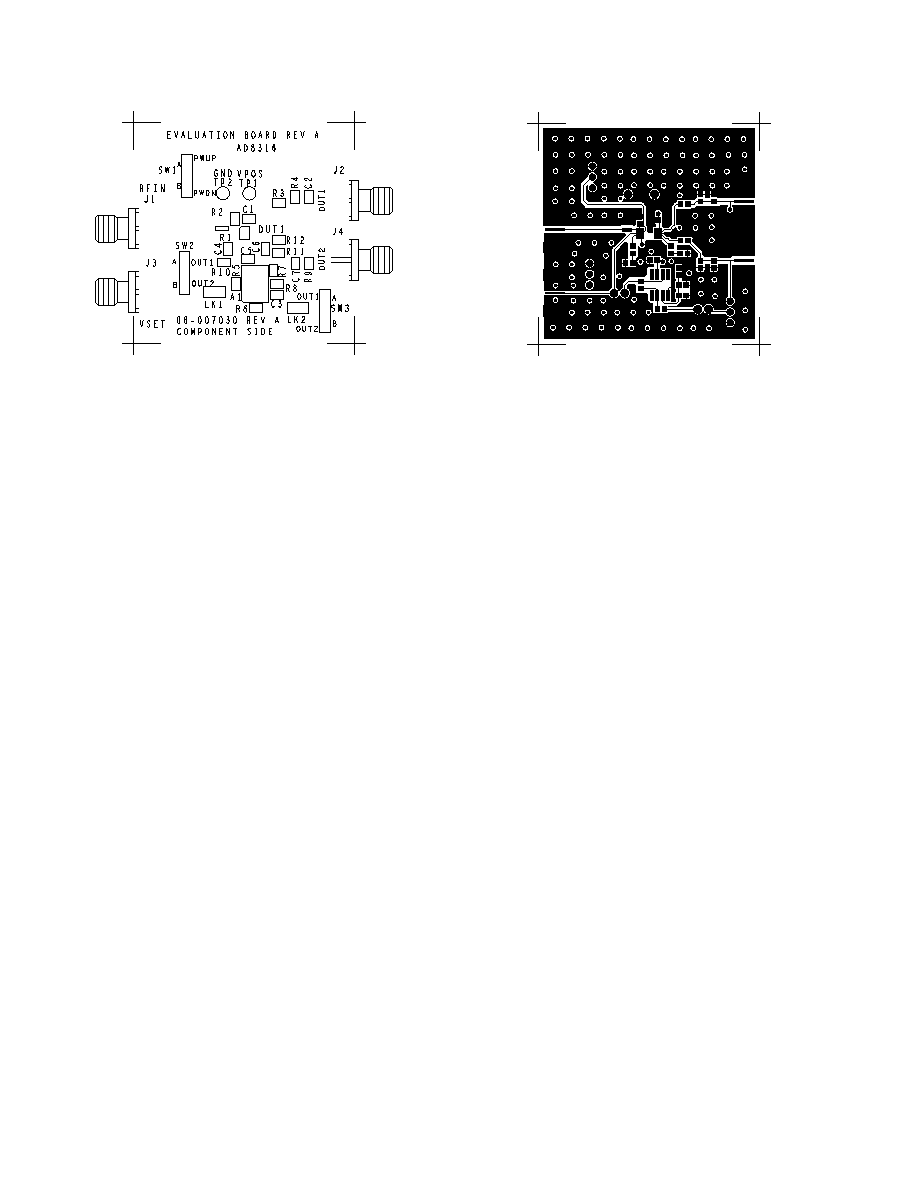
REV. C
≠18≠
AD8316
Figure 12. Silkscreen of Component Side (MSOP)
Figure 13. Layout of Component Side (MSOP)
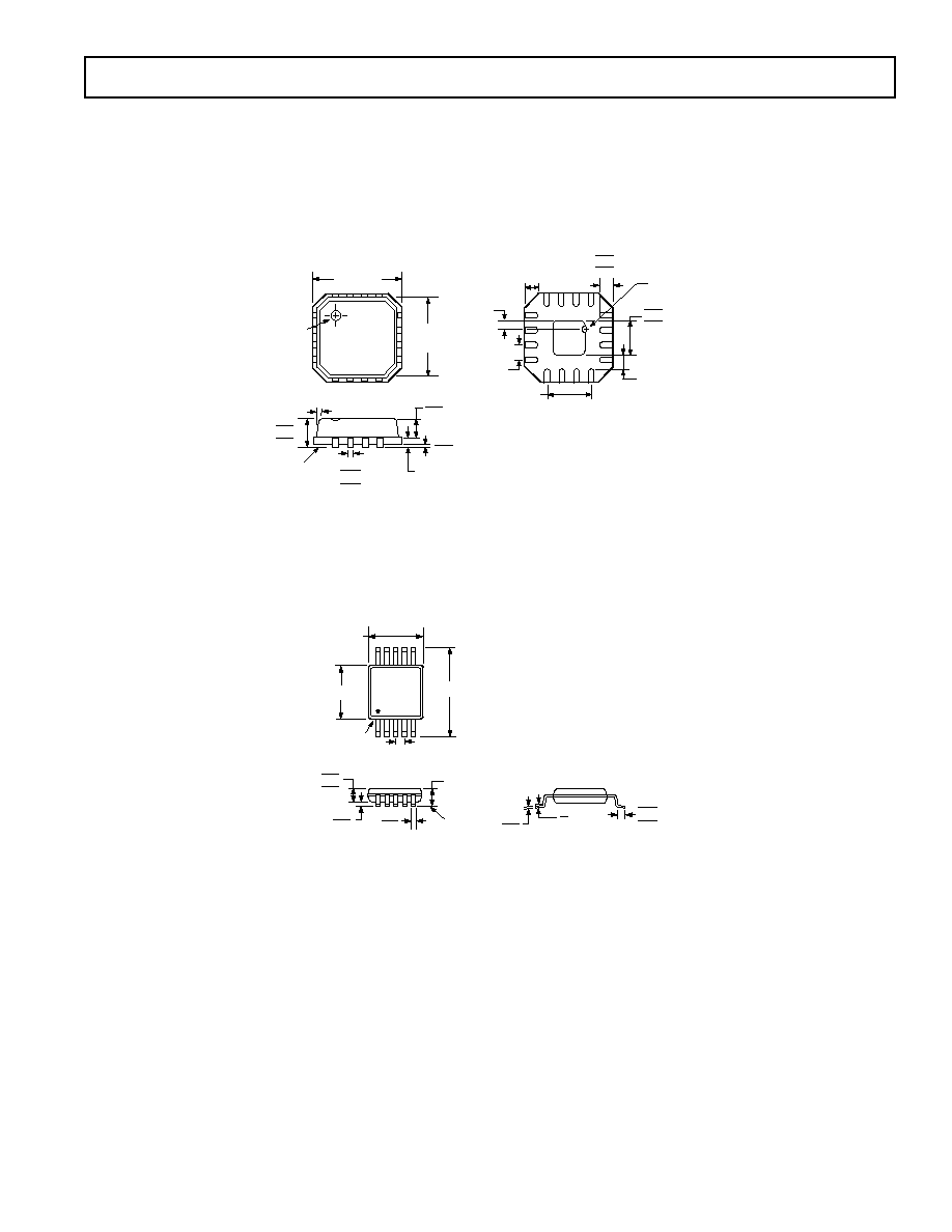
REV. C
AD8316
≠19≠
OUTLINE DIMENSIONS
16-Lead Lead Frame Chip Scale Package [LFCSP]
3 mm 3 mm Body
(CP-16-3)
Dimensions shown in millimeters
1
0.50
BSC
0.60 MAX
PIN 1 INDICATOR
1.50 REF
0.50
0.40
0.30
0.25 MIN
0.45
2.75
BSC SQ
TOP
VIEW
12
MAX
0.80 MAX
0.65 TYP
SEATING
PLANE
PIN 1
INDICATOR
1.00
0.85
0.80
0.30
0.23
0.18
0.05 MAX
0.02 NOM
0.20 REF
3.00
BSC SQ
1.65
1.50
1.35
BOTTOM
VIEW
SQ*
16
5
13
8
9
12
4
*COMPLIANT TO JEDEC STANDARDS MO-220-VEED-2
EXCEPT FOR EXPOSED PAD DIMENSION
10-Lead Mini Small Outline Package [MSOP]
(RM-10)
Dimensions shown in millimeters
0.23
0.08
0.80
0.60
0.40
8
0
0.15
0.00
0.27
0.17
0.95
0.85
0.75
SEATING
PLANE
1.10 MAX
10
6
5
1
0.50 BSC
3.00 BSC
3.00 BSC
4.90 BSC
PIN 1
COPLANARITY
0.10
COMPLIANT TO JEDEC STANDARDS MO-187BA

REV. C
C02192≠0≠1/04(C)
≠20≠
AD8316
Revision History
Location
Page
1/04≠Data Sheet changed from REV. B to REV. C.
Changes to FEATURES . . . . . . . . . . . . . . . . . . . . . . . . . . . . . . . . . . . . . . . . . . . . . . . . . . . . . . . . . . . . . . . . . . . . . . . . . . . . . . . . . . 1
12/03≠Data Sheet changed from REV. A to REV. B.
Updated ORDERING GUIDE . . . . . . . . . . . . . . . . . . . . . . . . . . . . . . . . . . . . . . . . . . . . . . . . . . . . . . . . . . . . . . . . . . . . . . . . . . . . . 3
Edit to Figure 8 . . . . . . . . . . . . . . . . . . . . . . . . . . . . . . . . . . . . . . . . . . . . . . . . . . . . . . . . . . . . . . . . . . . . . . . . . . . . . . . . . . . . . . . . 14
Updated OUTLINE DIMENSIONS . . . . . . . . . . . . . . . . . . . . . . . . . . . . . . . . . . . . . . . . . . . . . . . . . . . . . . . . . . . . . . . . . . . . . . . 19
3/03≠Data Sheet changed from REV. 0 to REV. A.
Addition of LFCSP package . . . . . . . . . . . . . . . . . . . . . . . . . . . . . . . . . . . . . . . . . . . . . . . . . . . . . . . . . . . . . . . . . . . . . . . . .Universal
Edits to SPECIFICATIONS . . . . . . . . . . . . . . . . . . . . . . . . . . . . . . . . . . . . . . . . . . . . . . . . . . . . . . . . . . . . . . . . . . . . . . . . . . . . . . . 2
Edits to ABSOLUTE MAXIMUM RATINGS . . . . . . . . . . . . . . . . . . . . . . . . . . . . . . . . . . . . . . . . . . . . . . . . . . . . . . . . . . . . . . . . . 3
Edits to ORDERING GUIDE . . . . . . . . . . . . . . . . . . . . . . . . . . . . . . . . . . . . . . . . . . . . . . . . . . . . . . . . . . . . . . . . . . . . . . . . . . . . . . 3
Edits to TPC 4 . . . . . . . . . . . . . . . . . . . . . . . . . . . . . . . . . . . . . . . . . . . . . . . . . . . . . . . . . . . . . . . . . . . . . . . . . . . . . . . . . . . . . . . . . 4
TPC 9 replaced . . . . . . . . . . . . . . . . . . . . . . . . . . . . . . . . . . . . . . . . . . . . . . . . . . . . . . . . . . . . . . . . . . . . . . . . . . . . . . . . . . . . . . . . . 5
Edit to TPC 30 . . . . . . . . . . . . . . . . . . . . . . . . . . . . . . . . . . . . . . . . . . . . . . . . . . . . . . . . . . . . . . . . . . . . . . . . . . . . . . . . . . . . . . . . . 8
Edits to Example section . . . . . . . . . . . . . . . . . . . . . . . . . . . . . . . . . . . . . . . . . . . . . . . . . . . . . . . . . . . . . . . . . . . . . . . . . . . . . . . . . 11
Edits to Input Coupling Options section . . . . . . . . . . . . . . . . . . . . . . . . . . . . . . . . . . . . . . . . . . . . . . . . . . . . . . . . . . . . . . . . . . . . . 15
Addition of new Figure 11 . . . . . . . . . . . . . . . . . . . . . . . . . . . . . . . . . . . . . . . . . . . . . . . . . . . . . . . . . . . . . . . . . . . . . . . . . . . . . . . . 16
Updated OUTLINE DIMENSIONS . . . . . . . . . . . . . . . . . . . . . . . . . . . . . . . . . . . . . . . . . . . . . . . . . . . . . . . . . . . . . . . . . . . . . . . 19