REV. B
Information furnished by Analog Devices is believed to be accurate and
reliable. However, no responsibility is assumed by Analog Devices for its
use, nor for any infringements of patents or other rights of third parties
which may result from its use. No license is granted by implication or
otherwise under any patent or patent rights of Analog Devices.
a
1-/2-/4-Channel
Digital Potentiometers
AD8400/AD8402/AD8403
One Technology Way, P.O. Box 9106, Norwood, MA 02062-9106, U.S.A.
Tel: 617/329-4700
World Wide Web Site: http://www.analog.com
Fax: 617/326-8703
© Analog Devices, Inc., 1997
FEATURES
256 Position
Replaces 1, 2 or 4 Potentiometers
1 k , 10 k , 50 k , 100 k
Power Shut Down--Less than 5 A
3-Wire SPI Compatible Serial Data Input
10 MHz Update Data Loading Rate
+2.7 V to +5.5 V Single-Supply Operation
Midscale Preset
APPLICATIONS
Mechanical Potentiometer Replacement
Programmable Filters, Delays, Time Constants
Volume Control, Panning
Line Impedance Matching
Power Supply Adjustment
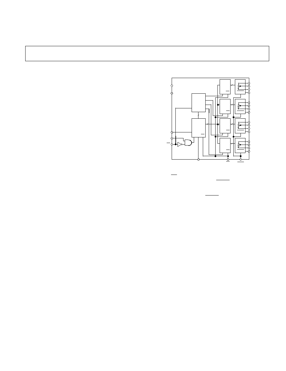
FUNCTIONAL BLOCK DIAGRAM
RDAC1
SHDN
8
8-BIT
LATCH
CK
RS
RDAC2
SHDN
8
8-BIT
LATCH
CK
RS
RDAC3
SHDN
8
8-BIT
LATCH
CK
RS
RDAC4
SHDN
8
8-BIT
LATCH
CK
RS
SHDN
DAC
SELECT
A1, A0
1
2
3
4
10-BIT
SERIAL
LATCH
CK Q
RS
D
RS
SDO
A1
W1
B1
AGND1
A2
W2
B2
AGND2
A3
W3
B3
AGND3
A4
W4
B4
AGND4
AD8403
V
DD
DGND
SDI
CLK
CS
8
2
GENERAL DESCRIPTION
The AD8400/AD8402/AD8403 provide a single, dual or quad
channel, 256 position digitally controlled variable resistor (VR)
device. These devices perform the same electronic adjustment
function as a potentiometer or variable resistor. The AD8400
contains a single variable resistor in the compact SO-8 package.
The AD8402 contains two independent variable resistors in
space saving SO-14 surface mount package. The AD8403 con-
tains four independent variable resistors in 24-lead PDIP, SOIC
and TSSOP packages. Each part contains a fixed resistor with a
wiper contact that taps the fixed resistor value at a point deter-
mined by a digital code loaded into the controlling serial input
register. The resistance between the wiper and either endpoint
of the fixed resistor varies linearly with respect to the digital
code transferred into the VR latch. Each variable resistor offers
a completely programmable value of resistance, between the A
terminal and the wiper or the B terminal and the wiper. The
fixed A to B terminal resistance of 1 k
, 10 k
, 50 k
or 100 k
has a
±
1% channel-to-channel matching tolerance with a nominal
temperature coefficient of 500 ppm/
∞
C. A unique switching cir-
cuit minimizes the high glitch inherent in traditional switched
resistor designs avoiding any make-before-break or break-before-
make operation.
Each VR has its own VR latch that holds its programmed
resistance value. These VR latches are updated from an SPI
compatible serial-to-parallel shift register that is loaded from a
standard 3-wire serial-input digital interface. Ten data bits make
up the data word clocked into the serial input register. The data
word is decoded where the first two bits determine the address
of the VR latch to be loaded, the last eight bits are data. A serial
data output pin at the opposite end of the serial register allows
simple daisy-chaining in multiple VR applications without addi-
tional external decoding logic.
The reset (RS) pin forces the wiper to the midscale position by
loading 80
H
into the VR latch. The SHDN pin forces the resis-
tor to an end-to-end open circuit condition on the A terminal
and shorts the wiper to the B terminal, achieving a microwatt
power shutdown state. When SHDN is returned to logic high,
the previous latch settings put the wiper in the same resistance
setting prior to shutdown. The digital interface is still active in
shutdown so that code changes can be made which will produce
new wiper positions when the device is taken out of shutdown.
The AD8400 is available in both the SO-8 surface mount and
the 8-lead plastic DIP package.
The AD8402 is available in both surface mount (SO-14) and
the 14-lead plastic DIP package, while the AD8403 is available
in a narrow body 24-lead plastic DIP and the 24-lead surface
mount package. The AD8402/AD8403 are also offered in the
1.1 mm thin TSSOP-14/TSSOP-24 package for PCMCIA ap-
plications. All parts are guaranteed to operate over the extended
industrial temperature range of ≠40
∞
C to +85
∞
C.
10 k VERSION
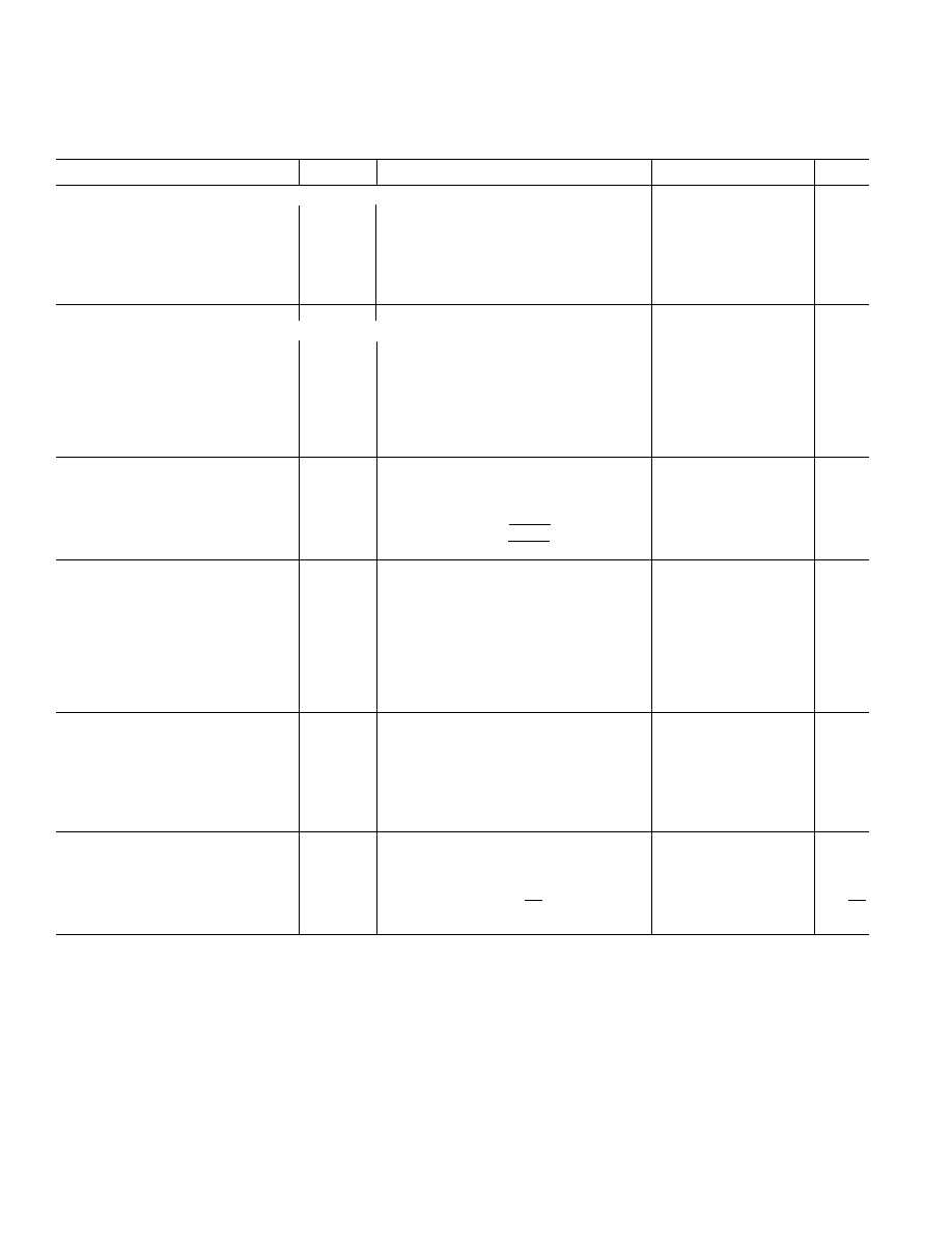
ELECTRICAL CHARACTERISTICS
Parameter
Symbol
Conditions
Min
Typ
1
Max
Units
DC CHARACTERISTICS RHEOSTAT MODE Specifications Apply to All VRs
Resistor Differential NL
2
R-DNL
R
WB
, V
A
= NC
≠1
±
1/4
+1
LSB
Resistor Nonlinearity
2
R-INL
R
WB
, V
A
= NC
≠2
±
1/2
+2
LSB
Nominal Resistance
3
R
T
A
= +25
∞
C, Model: AD840XYY10
8
10
12
k
Resistance Tempco
R
AB
/
T
V
AB
= V
DD
, Wiper = No Connect
500
ppm/
∞
C
Wiper Resistance
R
W
I
W
= 1 V/R
50
100
Nominal Resistance Match
R/R
O
CH 1 to 2, 3, or 4,
V
AB
= V
DD
, T
A
= +25
∞
C
0.2
1
%
DC CHARACTERISTICS POTENTIOMETER DIVIDER Specifications Apply to All VRs
Resolution
N
8
Bits
Integral Nonlinearity
4
INL
≠2
±
1/2
+2
LSB
Differential Nonlinearity
4
DNL
V
DD
= +5 V
≠1
±
1/4
+1
LSB
DNL
V
DD
= +3 V T
A
= +25
∞
C
≠1
±
1/4
+1
LSB
DNL
V
DD
= +3 V T
A
= ≠40
∞
C, +85
∞
C
≠1.5
±
1/2
+1.5
LSB
Voltage Divider Tempco
V
W
/
T
Code = 80
H
15
ppm/
∞
C
Full-Scale Error
V
WFSE
Code = FF
H
≠4
≠2.8
0
LSB
Zero-Scale Error
V
WZSE
Code = 00
H
0
+1.3
+2
LSB
RESISTOR TERMINALS
Voltage Range
5
V
A, B, W
0
V
DD
V
Capacitance
6
Ax, Bx
C
A, B
f = 1 MHz, Measured to GND, Code = 80
H
75
pF
Capacitance
6
Wx
C
W
f = 1 MHz, Measured to GND, Code = 80
H
120
pF
Shutdown Current
7
I
A_SD
V
A
= V
DD
, V
B
= 0 V, SHDN = 0
0.01
5
µ
A
Shutdown Wiper Resistance
R
W_SD
V
A
= V
DD
, V
B
= 0 V, SHDN = 0, V
DD
= +5 V
100
200
DIGITAL INPUTS & OUTPUTS
Input Logic High
V
IH
V
DD
= +5 V
2.4
V
Input Logic Low
V
IL
V
DD
= +5 V
0.8
V
Input Logic High
V
IH
V
DD
= +3 V
2.1
V
Input Logic Low
V
IL
V
DD
= +3 V
0.6
V
Output Logic High
V
OH
R
L
= 1 k
to V
DD
V
DD
≠0.1
V
Output Logic Low
V
OL
I
OL
= 1.6 mA, V
DD
= +5 V
0.4
V
Input Current
I
IL
V
IN
= 0 V or +5 V, V
DD
= +5 V
±
1
µ
A
Input Capacitance
6
C
IL
5
pF
POWER SUPPLIES
Power Supply Range
V
DD
Range
2.7
5.5
V
Supply Current (CMOS)
I
DD
V
IH
= V
DD
or V
IL
= 0 V
0.01
5
µ
A
Supply Current (TTL)
8
I
DD
V
IH
= 2.4 V or 0.8 V, V
DD
= +5.5 V
0.9
4
mA
Power Dissipation (CMOS)
9
P
DISS
V
IH
= V
DD
or V
IL
= 0 V, V
DD
= +5.5 V
27.5
µ
W
Power Supply Sensitivity
PSS
V
DD
= +5 V
±
10%
0.0002 0.001
%/%
PSS
V
DD
= +3 V
±
10%
0.006
0.03
%/%
DYNAMIC CHARACTERISTICS
6, 10
Bandwidth ≠3 dB
BW_10K
R = 10 k
600
kHz
Total Harmonic Distortion
THD
W
V
A
= 1 V rms + 2 V dc, V
B
= 2 V dc, f = 1 kHz
0.003
%
V
W
Settling Time
t
S
V
A
= V
DD
, V
B
= 0 V,
±
1% Error Band
2
µ
s
Resistor Noise Voltage
e
NWB
R
WB
= 5 k
, f = 1 kHz, RS = 0
9
nV/
Hz
Crosstalk
11
C
T
V
A
= V
DD
, V
B
= 0 V
≠65
dB
NOTES FOR 10 k
VERSION
1
Typicals represent average readings at +25
∞
C and V
DD
= +5 V.
2
Resistor position nonlinearity error R-INL is the deviation from an ideal value measured between the maximum resistance and the minimum resistance wiper
positions. R-DNL measures the relative step change from ideal between successive tap positions. Parts are guaranteed monotonic. See Figure 30 test circuit.
I
W
= 50
µ
A for V
DD
= +3 V and I
W
= 400
µ
A for V
DD
= +5 V for the 10 k
versions.
3
V
AB
= V
DD
, Wiper (V
W
) = No Connect.
4
INL and DNL are measured at V
W
with the RDAC configured as a potentiometer divider similar to a voltage output D/A converter. V
A
= V
DD
and V
B
= 0 V.
DNL Specification limits of
±
1 LSB maximum are Guaranteed Monotonic operating conditions. See Figure 29 test circuit.
5
Resistor terminals A, B, W have no limitations on polarity with respect to each other.
6
Guaranteed by design and not subject to production test. Resistor-terminal capacitance tests are measured with 2.5 V bias on the measured terminal. The remaining
resistor terminals are left open circuit.
7
Measured at the Ax terminals. All Ax terminals are open circuited in shutdown mode.
8
Worst case supply current consumed when input logic level at 2.4 V, standard characteristic of CMOS logic. See Figure 21 for a plot of I
DD
versus logic voltage.
9
P
DISS
is calculated from (I
DD
◊
V
DD
). CMOS logic level inputs result in minimum power dissipation.
10
All Dynamic Characteristics use V
DD
= +5 V.
11
Measured at a V
W
pin where an adjacent V
W
pin is making a full-scale voltage change.
Specifications subject to change without notice.
AD8400/AD8402/AD8403≠SPECIFICATIONS
(V
DD
= +3 V 10% or + 5 V 10%, V
A
= +V
DD
, V
B
= 0 V, ≠40 C
T
A
+85 C unless
otherwise noted)
REV. B
≠2≠

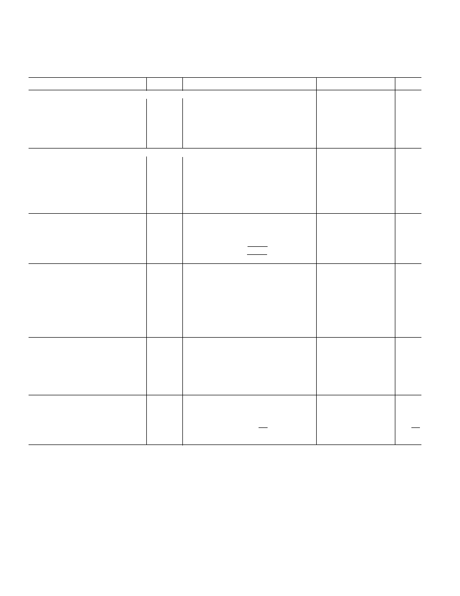
50 k & 100 k VERSION
ELECTRICAL CHARACTERISTICS
Parameter
Symbol
Conditions
Min
Typ
1
Max
Units
DC CHARACTERISTICS RHEOSTAT MODE Specifications Apply to All VRs
Resistor Differential NL
2
R-DNL
R
WB
, V
A
= NC
≠1
±
1/4
+1
LSB
Resistor Nonlinearity
2
R-INL
R
WB
, V
A
= NC
≠2
±
1/2
+2
LSB
Nominal Resistance
3
R
T
A
= +25
∞
C, Model: AD840XYY50
35
50
65
k
R
T
A
= +25
∞
C, Model: AD840XYY100
70
100
130
k
Resistance Tempco
R
AB
/
T
V
AB
= V
DD
, Wiper = No Connect
500
ppm/
∞
C
Wiper Resistance
R
W
I
W
= 1 V/R
53
100
Nominal Resistance Match
R/R
O
CH 1 to 2, 3, or 4,
V
AB
= V
DD
, T
A
= +25
∞
C
0.2
1
%
DC CHARACTERISTICS POTENTIOMETER DIVIDER Specifications Apply to All VRs
Resolution
N
8
Bits
Integral Nonlinearity
4
INL
≠4
±
1
+4
LSB
Differential Nonlinearity
4
DNL
V
DD
= +5 V
≠1
±
1/4
+1
LSB
DNL
V
DD
= +3 V T
A
= +25
∞
C
≠1
±
1/4
+1
LSB
DNL
V
DD
= +3 V T
A
= ≠40
∞
C, +85
∞
C
≠1.5
±
1/2
+1.5
LSB
Voltage Divider Tempco
V
W
/
T
Code = 80
H
15
ppm/
∞
C
Full-Scale Error
V
WFSE
Code = FF
H
≠1
≠0.25
0
LSB
Zero-Scale Error
V
WZSE
Code = 00
H
0
+0.1
+1
LSB
RESISTOR TERMINALS
Voltage Range
5
V
A, B, W
0
V
DD
V
Capacitance
6
Ax, Bx
C
A, B
f = 1 MHz, Measured to GND, Code = 80
H
15
pF
Capacitance
6
Wx
C
W
f = 1 MHz, Measured to GND, Code = 80
H
80
pF
Shutdown Current
7
I
A_SD
V
A
= V
DD
, V
B
= 0 V, SHDN = 0
0.01
5
µ
A
Shutdown Wiper Resistance
R
W_SD
V
A
= V
DD
, V
B
= 0 V, SHDN = 0, V
DD
= +5 V
100
200
DIGITAL INPUTS & OUTPUTS
Input Logic High
V
IH
V
DD
= +5 V
2.4
V
Input Logic Low
V
IL
V
DD
= +5 V
0.8
V
Input Logic High
V
IH
V
DD
= +3 V
2.1
V
Input Logic Low
V
IL
V
DD
= +3 V
0.6
V
Output Logic High
V
OH
R
L
= 1 k
to V
DD
V
DD
≠0.1
V
Output Logic Low
V
OL
I
OL
= 1.6 mA, V
DD
= +5 V
0.4
V
Input Current
I
IL
V
IN
= 0 V or +5 V, V
DD
= +5 V
±
1
µ
A
Input Capacitance
6
C
IL
5
pF
POWER SUPPLIES
Power Supply Range
V
DD
Range
2.7
5.5
V
Supply Current (CMOS)
I
DD
V
IH
= V
DD
or V
IL
= 0 V
0.01
5
µ
A
Supply Current (TTL)
8
I
DD
V
IH
= 2.4 V or 0.8 V, V
DD
= +5.5 V
0.9
4
mA
Power Dissipation (CMOS)
9
P
DISS
V
IH
= V
DD
or V
IL
= 0 V, V
DD
= +5.5 V
27.5
µ
W
Power Supply Sensitivity
PSS
V
DD
= +5 V
±
10%
0.0002 0.001
%/%
PSS
V
DD
= +3 V
±
10%
0.006
0.03
%/%
DYNAMIC CHARACTERISTICS
6, 10
Bandwidth ≠3 dB
BW_50K
R = 50 k
125
kHz
BW_100K
R = 100 k
71
kHz
Total Harmonic Distortion
THD
W
V
A
= 1 V rms + 2 V dc, V
B
= 2 V dc, f = 1 kHz
0.003
%
V
W
Settling Time
t
S
_50K
V
A
= V
DD
, V
B
= 0 V,
±
1% Error Band
9
µ
s
t
S
_100K
V
A
= V
DD
, V
B
= 0 V,
±
1% Error Band
18
µ
s
Resistor Noise Voltage
e
NWB
_50K
R
WB
= 25 k
, f = 1 kHz, RS = 0
20
nV/
Hz
e
NWB
_100K
R
WB
= 50 k
, f = 1 kHz, RS = 0
29
nV/
Hz
Crosstalk
11
C
T
V
A
= V
DD
, V
B
= 0 V
≠65
dB
NOTES FOR 50 k
and 100 k
VERSIONS
1
Typicals represent average readings at +25
∞
C and V
DD
= +5 V.
2
Resistor position nonlinearity error R-INL is the deviation from an ideal value measured between the maximum resistance and the minimum resistance wiper
positions. R-DNL measures the relative step change from ideal between successive tap positions. Parts are guaranteed monotonic. See Figure 30 test circuit.
I
W
= V
DD
/R for V
DD
= +3 V or +5 V for the 50 k
and 100 k
versions.
3
V
AB
= V
DD
, Wiper (V
W
) = No Connect.
4
INL and DNL are measured at V
W
with the RDAC configured as a potentiometer divider similar to a voltage output D/A converter. V
A
= V
DD
and V
B
= 0 V.
DNL Specification limits of
±
1 LSB maximum are Guaranteed Monotonic operating conditions. See Figure 29 test circuit.
5
Resistor terminals A, B, W have no limitations on polarity with respect to each other.
6
Guaranteed by design and not subject to production test. Resistor-terminal capacitance tests are measured with 2.5 V bias on the measured terminal. The remaining
resistor terminals are left open circuit.
7
Measured at the Ax terminals. All Ax terminals are open circuited in shutdown mode.
8
Worst case supply current consumed when input logic level at 2.4 V, standard characteristic of CMOS logic. See Figure 21 for a plot of I
DD
versus logic voltage.
9
P
DISS
is calculated from (I
DD
◊
V
DD
). CMOS logic level inputs result in minimum power dissipation.
10
All Dynamic Characteristics use V
DD
= +5 V.
11
Measured at a V
W
pin where an adjacent V
W
pin is making a full-scale voltage change.
Specifications subject to change without notice.
AD8400/AD8402/AD8403
REV. B
≠3≠
(V
DD
= +3 V 10% or + 5 V 10%, V
A
= +V
DD
, V
B
= 0 V, ≠40 C
T
A
+85 C unless
otherwise noted)
SPECIFICATIONS
1 k VERSION
ELECTRICAL CHARACTERISTICS
Parameter
Symbol
Conditions
Min
Typ
1
Max
Units
DC CHARACTERISTICS RHEOSTAT MODE Specifications Apply to All VRs
Resistor Differential NL
2
R-DNL
R
WB
, V
A
= NC
≠5
≠1
+3
LSB
Resistor Nonlinearity
2
R-INL
R
WB
, V
A
= NC
≠4
±
1.5
+4
LSB
Nominal Resistance
3
R
T
A
= +25
∞
C, Model: AD840XYY1
0.8
1.2
1.5
k
Resistance Tempco
R
AB
/
T
V
AB
= V
DD
, Wiper = No Connect
700
ppm/
∞
C
Wiper Resistance
R
W
I
W
= 1 V/R
AB
53
100
Nominal Resistance Match
R/R
O
CH 1 to 2,
V
AB
= V
DD
, T
A
= +25
∞
C
0.75
2
%
DC CHARACTERISTICS POTENTIOMETER DIVIDER Specifications Apply to All VRs
Resolution
N
8
Bits
Integral Nonlinearity
4
INL
≠6
±
2
+6
LSB
Differential Nonlinearity
4
DNL
V
DD
= +5 V
≠4
≠1.5
+2
LSB
DNL
V
DD
= +3 V, T
A
= +25
∞
C
≠5
≠2
+5
LSB
Voltage Divider Temperature Coefficent
V
W
/
T
Code = 80
H
25
ppm/
∞
C
Full-Scale Error
V
WFSE
Code = FF
H
≠20
≠12
0
LSB
Zero-Scale Error
V
WZSE
Code = 00
H
0
6
10
LSB
RESISTOR TERMINALS
Voltage Range
5
V
A, B, W
0
V
DD
V
Capacitance
6
Ax, Bx
C
A, B
f = 1 MHz, Measured to GND, Code = 80
H
75
pF
Capacitance
6
Wx
C
W
f = 1 MHz, Measured to GND, Code = 80
H
120
pF
Shutdown Supply Current
7
I
DD_SD
V
A
= V
DD
, V
B
= 0 V, SHDN = 0
0.01
5
µ
A
Shutdown Wiper Resistance
R
W_SD
V
A
= V
DD
, V
B
= 0 V, SHDN = 0, V
DD
= +5 V
50
100
DIGITAL INPUTS & OUTPUTS
Input Logic High
V
IH
V
DD
= +5 V
2.4
V
Input Logic Low
V
IL
V
DD
= +5 V
0.8
V
Input Logic High
V
IH
V
DD
= +3 V
2.1
V
Input Logic Low
V
IL
V
DD
= +3 V
0.6
V
Output Logic High
V
OH
R
L
= 1 k
to V
DD
V
DD
≠0.1
V
Output Logic Low
V
OL
I
OL
= 1.6 mA, V
DD
= +5 V
0.4
V
Input Current
I
IL
V
IN
= 0 V or +5 V, V
DD
= +5 V
±
1
µ
A
Input Capacitance
6
C
IL
5
pF
POWER SUPPLIES
Power Supply Range
V
DD
Range
2.7
5.5
V
Supply Current (CMOS)
I
DD
V
IH
= V
DD
or V
IL
= 0 V
0.01
5
µ
A
Supply Current (TTL)
8
I
DD
V
IH
= 2.4 V or 0.8 V, V
DD
= +5.5 V
0.9
4
mA
Power Dissipation (CMOS)
9
P
DISS
V
IH
= V
DD
or V
IL
= 0 V, V
DD
= +5.5 V
27.5
µ
W
Power Supply Sensitivity
PSS
V
DD
= +5 V
±
10%
0.0035 0.008
%/%
PSS
V
DD
= +3 V
±
10%
0.05
0.13
%/%
DYNAMIC CHARACTERISTICS
6, 10
Bandwidth ≠3 dB
BW_1K
R = 1 k
5,000
kHz
Total Harmonic Distortion
THD
W
V
A
= 1 V rms + 2 V dc, V
B
= 2 V dc, f = 1 kHz
0.015
%
V
W
Settling Time
t
S
V
A
= V
DD
, V
B
= 0 V,
±
1% Error Band
0.5
µ
s
Resistor Noise Voltage
e
NWB
R
WB
= 500
, f = 1 kHz, RS = 0
3
nV/
Hz
Crosstalk
11
C
T
V
A
= V
DD
, V
B
= 0 V
≠65
dB
NOTES FOR 1 k
VERSION
1
Typicals represent average readings at +25
∞
C and V
DD
= +5 V.
2
Resistor position nonlinearity error R-INL is the deviation from an ideal value measured between the maximum resistance and the minimum resistance wiper
positions. R-DNL measures the relative step change from ideal between successive tap positions. See Figure 30 test circuit.
I
W
= 500
µ
A for V
DD
= +3 V and I
W
= 4 mA for V
DD
= +5 V for 1 k
version.
3
V
AB
= V
DD
, Wiper (V
W
) = No Connect.
4
INL and DNL are measured at V
W
with the RDAC configured as a potentiometer divider similar to a voltage output D/A converter. V
A
= V
DD
and V
B
= 0 V.
DNL Specification limits of
±
1 LSB maximum are Guaranteed Monotonic operating conditions. See Figure 29 test circuit.
5
Resistor terminals A, B, W have no limitations on polarity with respect to each other.
6
Guaranteed by design and not subject to production test. Resistor-terminal capacitance tests are measured with 2.5 V bias on the measured terminal. The remaining
resistor terminals are left open circuit.
7
Measured at the Ax terminals. All Ax terminals are open circuited in shutdown mode.
8
Worst case supply current consumed when input logic level at 2.4 V, standard characteristic of CMOS logic. See Figure 21 for a plot of I
DD
versus logic voltage.
9
P
DISS
is calculated from (I
DD
◊
V
DD
). CMOS logic level inputs result in minimum power dissipation.
10
All Dynamic Characteristics use V
DD
= +5 V.
11
Measured at a V
W
pin where an adjacent V
W
pin is making a full-scale voltage change.
Specifications subject to change without notice.
AD8400/AD8402/AD8403≠SPECIFICATIONS
(V
DD
= +3 V 10% or + 5 V 10%, V
A
= +V
DD
, V
B
= 0 V, ≠40 C
T
A
+85 C unless
otherwise noted)
≠4≠
REV. B

All VERSIONS
ELECTRICAL CHARACTERISTICS
Parameter
Symbol
Conditions
Min
Typ
1
Max
Units
SWITCHING CHARACTERISTICS
2, 3
Input Clock Pulse Width
t
CH
, t
CL
Clock Level High or Low
10
ns
Data Setup Time
t
DS
5
ns
Data Hold Time
t
DH
5
ns
CLK to SDO Propagation Delay
4
t
PD
R
L
= 1 k
to +5 V, C
L
20 pF
1
25
ns
CS
Setup Time
t
CSS
10
ns
CS
High Pulse Width
t
CSW
10
ns
Reset Pulse Width
t
RS
50
ns
CLK Fall to CS Rise Hold Time
t
CSH
0
ns
CS
Rise to Clock Rise Setup
t
CS1
10
ns
NOTES
1
Typicals represent average readings at +25
∞
C and V
DD
= +5 V.
2
Guaranteed by design and not subject to production test. Resistor-terminal capacitance tests are measured with 2.5 V bias on the measured terminal. The remaining
resistor terminals are left open circuit.
3
See timing diagram for location of measured values. All input control voltages are specified with t
R
= t
F
= 1 ns (10% to 90% of V
DD
) and timed from a voltage level
of 1.6 V. Switching characteristics are measured using V
DD
= +3 V or +5 V. To avoid false clocking a minimum input logic slew rate of 1 V/
µ
s should be maintained.
4
Propagation Delay depends on value of V
DD
, R
L
and C
L
≠see applications text.
Specifications subject to change without notice.
AD8400/AD8402/AD8403≠SPECIFICATIONS
WARNING!
ESD SENSITIVE DEVICE
CAUTION
ESD (electrostatic discharge) sensitive device. Electrostatic charges as high as 4000 V readily
accumulate on the human body and test equipment and can discharge without detection.
Although the AD8400/AD8402/AD8403 feature proprietary ESD protection circuitry, perma-
nent damage may occur on devices subjected to high energy electrostatic discharges. Therefore,
proper ESD precautions are recommended to avoid performance degradation or loss of functionality.
(V
DD
= +3 V 10% or + 5 V 10%, V
A
= +V
DD
, V
B
= 0 V, ≠40 C
T
A
+85 C unless
otherwise noted)
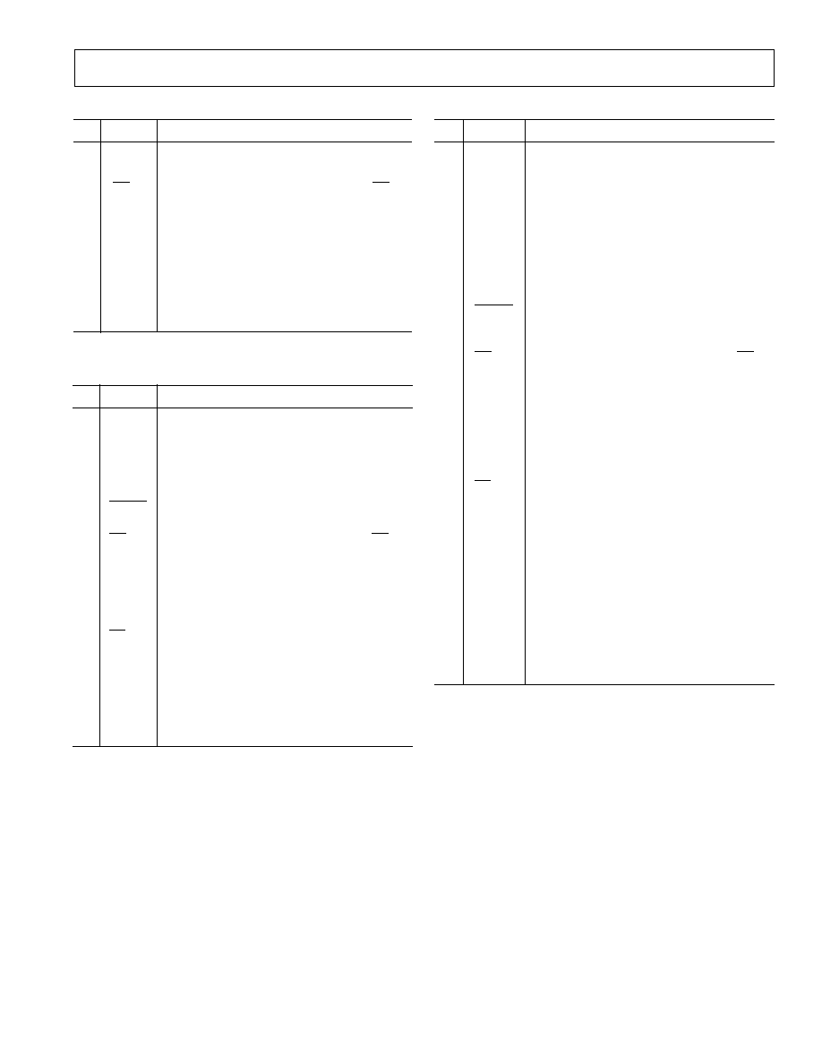
DAC REGISTER LOAD
A1
A0
D7
D6
D5
D4
D3
D2
D1
D0
1
0
1
0
1
0
V
DD
0V
SDI
CLK
CS
V
OUT
Figure 1a. Timing Diagram
±
1 % ERROR BAND
±
1 %
t
CSH
t
CSS
t
DH
Ax OR Dx
Ax OR Dx
t
PD_MIN
t
PD_MAX
A'x OR D'x
A'x OR D'x
1
0
1
0
1
0
V
DD
0V
SDI
(DATA IN)
CLK
CS
V
OUT
1
0
SDO
(DATA OUT)
t
DS
t
CH
t
CS1
t
CL
t
S
t
CSW
Figure 1b. Detail Timing Diagram
±
1%
±
1% ERROR BAND
RS
1
0
V
DD
V
DD
/2
V
OUT
t
RS
t
S
Figure 1c. Reset Timing Diagram
≠5≠
REV. B
ABSOLUTE MAXIMUM RATINGS*
(T
A
= +25
∞
C, unless otherwise noted)
V
DD
to GND . . . . . . . . . . . . . . . . . . . . . . . . . . . . ≠0.3 V, +8 V
V
A
, V
B
, V
W
to GND . . . . . . . . . . . . . . . . . . . . . . . . . . 0 V, V
DD
A
X
≠B
X
, A
X
≠W
X
, B
X
≠W
X
. . . . . . . . . . . . . . . . . . . . . .
±
20 mA
Digital Input and Output Voltage to GND . . . . . . . 0 V, +8 V
Operating Temperature Range . . . . . . . . . . . . ≠40
∞
C to +85
∞
C
Maximum Junction Temperature (T
J
max) . . . . . . . . . +150
∞
C
Storage Temperature . . . . . . . . . . . . . . . . . . ≠65
∞
C to +150
∞
C
Lead Temperature (Soldering, 10 sec) . . . . . . . . . . . . . +300
∞
C
Package Power Dissipation . . . . . . . . . . . . . . (T
J
max≠T
A
)/
JA
Thermal Resistance
(
JA
)
P-DIP (N-14) . . . . . . . . . . . . . . . . . . . . . . . . . . . . +83
∞
C/W
P-DIP (N-24) . . . . . . . . . . . . . . . . . . . . . . . . . . . . +63
∞
C/W
SOIC (SO-14) . . . . . . . . . . . . . . . . . . . . . . . . . . . +70
∞
C/W
SOIC (SOL-24) . . . . . . . . . . . . . . . . . . . . . . . . . +120
∞
C/W
TSSOP-14 (RU-14) . . . . . . . . . . . . . . . . . . . . . . +180
∞
C/W
TSSOP-24 (RU-24) . . . . . . . . . . . . . . . . . . . . . . +143
∞
C/W
*Stresses above those listed under "Absolute Maximum Ratings" may cause
permanent damage to the device. This is a stress rating only; functional operation
of the device at these or any other conditions above those listed in the operational
sections of this specification is not implied. Exposure to absolute maximum rating
conditions for extended periods may affect device reliability.

AD8400/AD8402/AD8403
≠6≠
REV. B
Table I. Serial Data Word Format
ADDR
DATA
B9
B8
B7
B6
B5
B4
B3
B2
B1
B0
A1
A0
D7
D6
D5
D4
D3
D2
D1
D0
MSB
LSB
MSB
LSB
2
9
2
8
2
7
2
0
PIN CONFIGURATIONS
1
2
3
4
8
7
6
5
TOP VIEW
(Not to Scale)
AD8400
B1
CLK
V
DD
W1
A1
GND
CS
SDI
14
13
12
11
10
9
8
1
2
3
4
7
6
5
TOP VIEW
(Not to Scale)
AGND
V
DD
W1
A1
B1
B2
A2
W2
AD8402
SDI
CLK
RS
DGND
SHDN
CS
13
16
15
14
24
23
22
21
20
19
18
17
TOP VIEW
(Not to Scale)
12
11
10
9
8
1
2
3
4
7
6
5
AD8403
AGND2
AGND1
W1
A1
B1
B2
A2
W2
W3
A3
B3
AGND4
B4
A4
W4
DGND
SHDN
RS
V
DD
AGND3
CS
SDI
CLK
SDO
ORDERING GUIDE
#CHs/
Temperature
Package
Package
Model
k
Range
Description Option*
AD8400AN10
X1/10
-40
∞
C to +85
∞
C
PDIP-8
N-8
AD8400AR10
X1/10
-40
∞
C to +85
∞
C
SO-8
SO-8
AD8402AN10
X2/10
-40
∞
C to +85
∞
C
PDIP-14
N-14
AD8402AR10
X2/10
-40
∞
C to +85
∞
C
SO-14
SO-14
AD8402ARU10
X2/10
-40
∞
C to +85
∞
C
TSSOP-14
RU-14
AD8403AN10
X4/10
-40
∞
C to +85
∞
C
PDIP-24
N-24
AD8403AR10
X4/10
-40
∞
C to +85
∞
C
SOIC-24
SOL-24
AD8403ARU10
X4/10
-40
∞
C to +85
∞
C
TSSOP-24
RU-24
AD8400AN50
X1/50
-40
∞
C to +85
∞
C
PDIP-8
N-8
AD8400AR50
X1/50
-40
∞
C to +85
∞
C
SO-8
SO-8
AD8402AN50
X2/50
-40
∞
C to +85
∞
C
PDIP-14
N-14
AD8402AR50
X2/50
-40
∞
C to +85
∞
C
SO-14
SO-14
AD8403AN50
X4/50
-40
∞
C to +85
∞
C
PDIP-24
N-24
AD8403AR50
X4/50
-40
∞
C to +85
∞
C
SOIC-24
SOL-24
AD8400AN100
X1/100
-40
∞
C to +85
∞
C
PDIP-8
N-8
AD8400AR100
X1/100
-40
∞
C to +85
∞
C
SO-8
SO-8
AD8402AN100
X2/100
-40
∞
C to +85
∞
C
PDIP-14
N-14
AD8402AR100
X2/100
-40
∞
C to +85
∞
C
SO-14
SO-14
AD8402ARU100
X2/100
-40
∞
C to +85
∞
C
TSSOP-14
RU-14
AD8403AN100
X4/100
-40
∞
C to +85
∞
C
PDIP-24
N-24
AD8403AR100
X4/100
-40
∞
C to +85
∞
C
SOIC-24
SOL-24
AD8403ARU100
X4/100
-40
∞
C to +85
∞
C
TSSOP-24
RU-24
AD8400AN1
X1/1
-40
∞
C to +85
∞
C
PDIP-8
N-8
AD8400AR1
X1/1
-40
∞
C to +85
∞
C
SO-8
SO-8
AD8402AN1
X2/1
-40
∞
C to +85
∞
C
PDIP-14
N-14
AD8402AR1
X2/1
-40
∞
C to +85
∞
C
SO-14
SO-14
AD8403AN1
X4/1
-40
∞
C to +85
∞
C
PDIP-24
N-24
AD8403AR1
X4/1
-40
∞
C to +85
∞
C
SOIC-24
SOL-24
AD8403ARU1
X4/1
-40
∞
C to +85
∞
C
TSSOP-24
RU-24
*N = Plastic DIP; SO = Small Outline; RU = Thin Shrink SO.
The AD8400, AD8402 and the AD8403 contain 720 transistors.
AD8400/AD8402/AD8403
REV. B
≠7≠
AD8400 PIN DESCRIPTIONS
Pin
Name
Description
1
B1
Terminal B RDAC
2
GND
Ground
3
CS
Chip Select Input, Active Low. When CS
returns high data in the serial input register is
loaded into the DAC register.
4
SDI
Serial Data Input
5
CLK
Serial Clock Input, positive edge triggered
6
V
DD
Positive power supply, specified for operation
at both +3 V and +5 V.
7
W1
Wiper RDAC, addr = 00
2
8
A1
Terminal A RDAC
AD8402 PIN DESCRIPTIONS
Pin
Name
Description
1
AGND
Analog Ground*
2
B2
Terminal B RDAC #2
3
A2
Terminal A RDAC #2
4
W2
Wiper RDAC #2, Addr = 01
2
5
DGND
Digital Ground*
6
SHDN
Terminal A open circuit. Shutdown controls
Variable Resistors #1 and #2
7
CS
Chip Select Input, Active Low. When CS
returns high data in the serial input register is
decoded based on the address bits and loaded
into the target DAC register.
8
SDI
Serial Data Input
9
CLK
Serial Clock Input, positive edge triggered
10
RS
Active low reset to midscale; sets RDAC
registers to 80
H
11
V
DD
Positive power supply, specified for operation
at both +3 V and +5 V
12
W1
Wiper RDAC #1, addr = 00
2
13
A1
Terminal A RDAC #1
14
B1
Terminal B RDAC #1
*All AGNDs must be connected to DGND.
AD8403 PIN DESCRIPTIONS
Pin
Name
Description
1
AGND2
Analog Ground #2*
2
B2
Terminal B RDAC #2
3
A2
Terminal A RDAC #2
4
W2
Wiper RDAC #2, addr = 01
2
5
AGND4
Analog Ground #4*
6
B4
Terminal B RDAC #4
7
A4
Terminal A RDAC #4
8
W4
Wiper RDAC #4, addr = 11
2
9
DGND
Digital Ground*
10
SHDN
Active Low Input. Terminal A open circuit.
Shutdown controls variable resistors #1
through #4
11
CS
Chip Select Input, Active Low. When CS
returns high data in the serial input register
is decoded based on the address bits and
loaded into the target DAC register.
12
SDI
Serial Data Input
13
SDO
Serial Data Output, Open Drain transistor
requires pull-up resistor
14
CLK
Serial Clock Input, positive edge triggered
15
RS
Active low reset to midscale; sets RDAC
registers to 80
H
16
V
DD
Positive power supply, specified for
operation at both +3 V and +5 V
17
AGND3
Analog Ground #3*
18
W3
Wiper RDAC #3, addr = 10
2
19
A3
Terminal A RDAC #3
20
B3
Terminal B RDAC #3
21
AGND1
Analog Ground #1*
22
W1
Wiper RDAC #1, addr = 00
2
23
A1
Terminal A RDAC #1
24
B1
Terminal B RDAC #1
*All AGNDs must be connected to DGND.
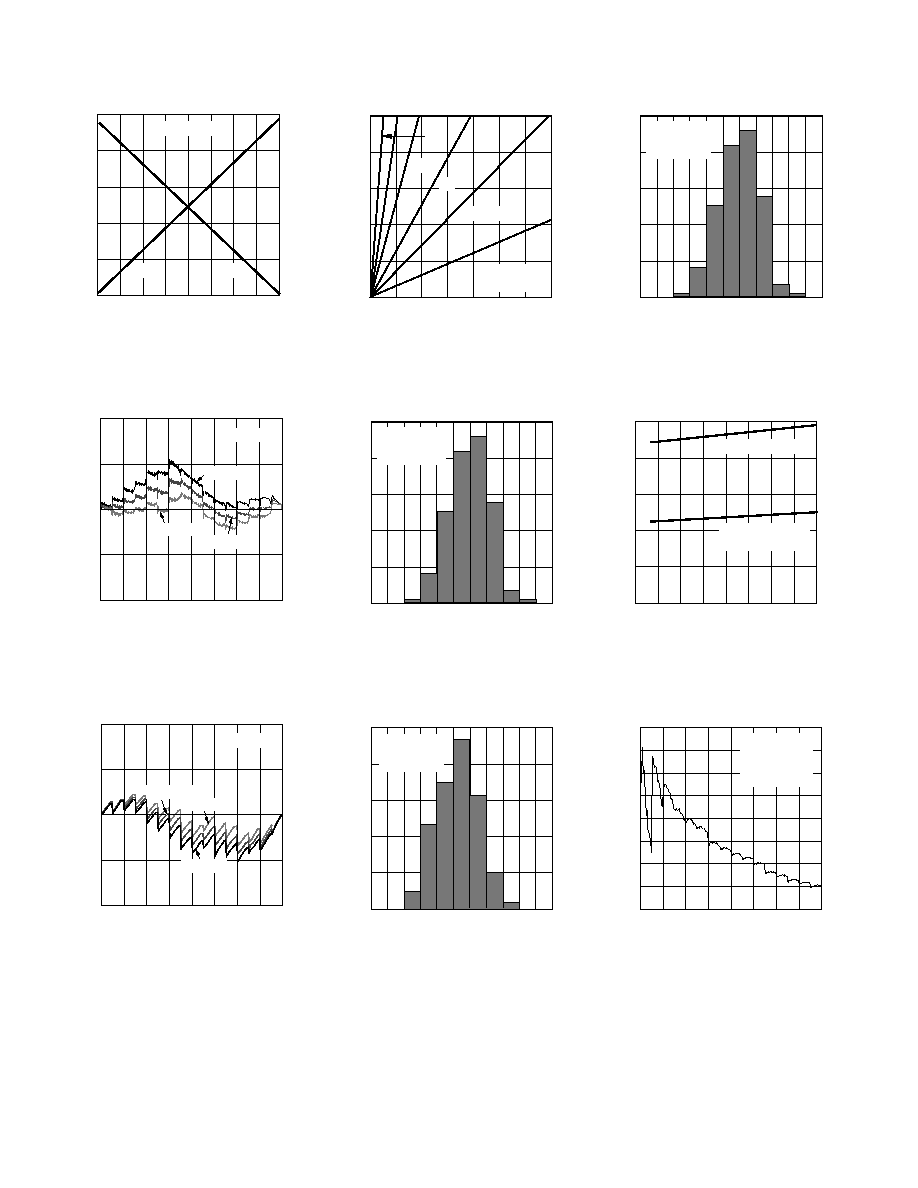
CODE ≠ Decimal
10
8
0
0
32
256
64
96
128
160
192
224
6
4
2
RESISTANCE ≠ k
V
DD
= +3V OR +5V
R
WB
R
WA
Figure 2. Wiper to End Terminal
Resistance vs. Code
DIGITAL INPUT CODE ≠ Decimal
1
0.5
≠1
0
32
256
64
96
128
160
192
224
0
≠0.5
V
DD
= +5V
T
A
= ≠40
∞
C
T
A
= +25
∞
C
T
A
= +85
∞
C
R-INL ERROR ≠ LSB
Figure 5. Resistance Step Position
Nonlinearity Error vs. Code
DIGITAL INPUT CODE ≠ Decimal
1
0.5
≠1
0
32
256
64
96
128
160
192
224
0
≠0.5
INL NONLINEARITY ERROR ≠ LSB
T
A
= ≠40
∞
C
T
A
= +25
∞
C
T
A
= +85
∞
C
V
DD
= +5V
Figure 8. Potentiometer Divider
Nonlinearity Error vs. Code
AD8400/AD8402/AD8403≠Typical Performance Characteristics
I
WA
CURRENT ≠ mA
5
4
0
0
7
1
4
5
3
2
1
2
3
6
80
H
40
H
20
H
FF
H
CODE = 10
H
T
A
= +25
∞
C
V
DD
= +5V
V
WB
VOLTAGE ≠ V
05
H
Figure 3. Resistance Linearity vs.
Conduction Current
WIPER RESISTANCE ≠
FREQUENCY
60
48
0
40.0 42.5
65.0
45.0 47.5 50.0 52.5 55.0 57.5 60.0 62.5
36
24
12
SS = 1205 UNITS
V
DD
= 4.5V
T
A
= +25
∞
C
Figure 6. 10 k
Wiper-Contact-
Resistance Histogram
WIPER RESISTANCE ≠
FREQUENCY
60
48
0
35
37
55
39
41
43
45
47
49
51
53
36
24
12
SS = 184 UNITS
V
DD
= 4.5V
T
A
= +25
∞
C
Figure 9. 50 k
Wiper-Contact-
Resistance Histogram
WIPER RESISTANCE ≠
FREQUENCY
60
48
0
40.0 42.5
65.0
45.0 47.5 50.0 52.5 55.0 57.5 60.0 62.5
36
24
12
SS = 184 UNITS
V
DD
= 4.5V
T
A
= +25
∞
C
Figure 4. 100 k
Wiper-Contact-
Resistance Histogram
TEMPERATURE ≠
∞
C
NOMINAL RESISTANCE ≠
10
8
0
≠75
≠50
125
≠25
0
25
50
75
100
6
4
2
R
AB
(END-TO-END)
R
WB
(WIPER-TO-END)
CODE = 80
H
Figure 7. Nominal Resistance vs.
Temperature
CODE ≠ DECIMAL
POTENTIOMETER MODE TEMPCO ≠ ppm/C
∞
70
60
≠10
0
32
160
64
96
128
30
20
10
0
50
40
192 224 256
V
DD
= +5V
T
A
= ≠40
∞
C/+85
∞
C
V
A
= 2.00V
V
B
= 0V
Figure 10.
V
WB
/ T Potentiometer
Mode Tempco
≠8≠
REV. B
AD8400/AD8402/AD8403
REV. B
≠9≠
TIME = 5
µ
s/DIV
Figure 15. Large Signal Settling
Time
TIME 200ns/DIV
Figure 18. Digital Feedthrough
vs. Time
FREQUENCY ≠ Hz
6
0
≠54
GAIN ≠ dB
10
1M
100
1k
10k
100k
≠6
≠12
≠48
≠18
≠24
≠30
≠36
≠42
CODE = FF
80
40
20
10
08
04
02
01
T
A
= +25
∞
C
SEE TEST FIGURE 33
Figure 13. Gain vs. Frequency for
R = 10 k
FREQUENCY ≠ Hz
GAIN ≠ dB
0
≠6
≠48
1k
10k
1M
≠30
≠36
≠42
≠12
≠24
≠18
≠54
100k
6
CODE = FF
H
80
H
40
H
20
H
10
H
08
H
04
H
02
H
01
H
Figure 16. 50 k
Gain vs. Fre-
quency vs. Code
FREQUENCY ≠ Hz
GAIN ≠ dB
0
≠6
≠48
1k
10k
1M
≠30
≠36
≠42
≠12
≠24
≠18
≠54
100k
CODE = FF
H
6
80
H
40
H
20
H
10
H
08
H
04
H
02
H
01
H
Figure 19. 100 k
Gain vs. Fre-
quency vs. Code
OUTPUT
INPUT
V
OUT
(50mV/DIV)
R
W
(20mV/DIV)
CS
(5V/DIV)
CODE ≠ DECIMAL
700
600
≠100
0
32
160
64
96
128
300
200
100
0
500
400
192 224 256
RHEOSTAT MODE TEMPCO ≠ ppm/C
∞
V
DD
= +5V
T
A
= ≠40
∞
C/+85
∞
C
V
A
= NO CONNECT
R
WB
MEASURED
Figure 11.
R
WB
/ T Rheostat Mode
Tempco
HOURS OF OPERATION AT 150
∞
C
0.75
0.5
≠0.75
0
600
100
300
400
0.25
≠0.25
≠0.5
200
500
CODE = 80
H
V
DD
= +5V
SS = 158 UNITS
0
R
WB
RESISTANCE ≠ %
AVG + 2 SIGMA
AVG
AVG ≠ 2 SIGMA
Figure 14. Long-Term Drift
Accelerated by Burn-In
FREQUENCY ≠ Hz
THD + NOISE ≠ %
10
0.001
10
100k
100
1k
10k
1
0.1
FILTER = 22kHz
V
DD
= +5V
T
A
= +25
∞
C
0.01
SEE TEST CIRCUIT FIGURE 32
SEE TEST CIRCUIT FIGURE 31
Figure 17. Total Harmonic Distortion
Plus Noise vs. Frequency
Figure 12. One Position Step Change
at Half-Scale (Code 7F
H
to 80
H
)
TIME 500ns/DIV

AD8400/AD8402/AD8403
≠10≠
REV. B
FREQUENCY ≠ Hz
10
10k
1M
NORMALIZED GAIN FLATNESS ≠ 0.1dB/DIV
100k
100
1k
SEE TEST CIRCUIT 33
CODE = 80
H
V
DD
= +5V
T
A
= +25
∞
C
R = 10k
R = 50k
R = 100k
Figure 20. Normalized Gain Flat-
ness vs. Frequency
FREQUENCY ≠ Hz
GAIN ≠ dB
0
≠6
1k
10k
1M
≠30
≠36
≠42
≠12
≠24
≠18
100k
V
IN
= 100mV rms
V
DD
= +5V
R
L
= 1M
6
12
f
≠3dB
= 125kHz, R = 50k
f
≠3dB
= 700kHz, R = 10k
f
≠3dB
= 71kHz, R = 100k
Figure 23. ≠3 dB Bandwidths
FREQUENCY ≠ Hz
100k
2M
200k
1M
0
≠10
≠20
0
≠45
≠90
400k
4M 6M
PHASE ≠ Degrees
10M
GAIN ≠ dB
V
DD
= +5V
T
A
= +25
∞
C
WIPER SET AT
HALF-SCALE 80
H
Figure 26. 1 k
Gain and Phase
vs. Frequency
INPUT LOGIC VOLTAGE ≠ Volts
I
DD
≠ SUPPLY CURRENT ≠ mA
10
1
0.01
0
5
1
2
3
4
0.1
T
A
= +25
∞
C
V
DD
= +5V
V
DD
= +3V
Figure 21. Supply Current vs. Logic
Input Voltage
FREQUENCY ≠ Hz
1k
1M
10M
10k
100k
I
DD
≠ SUPPLY CURRENT ≠ µA
1200
1000
800
600
400
200
0
T
A
= +25
∞
C
A
B
C
D
A ≠ V
DD
= 5.5V
CODE = 55
H
B ≠ V
DD
= 3.3V
CODE = 55
H
C ≠ V
DD
= 5.5V
CODE = FF
H
D ≠ V
DD
= 3.3V
CODE = FF
H
Figure 24. Supply Current vs.
Clock Frequency
I
A
SHUTDOWN CURRENT ≠ nA
100
1
≠55 ≠35
10
V
DD
= +5V
≠15
5
25
45
65
85
105 125
TEMPERATURE ≠
∞
C
Figure 27. Shutdown Current vs.
Temperature
FREQUENCY ≠ Hz
PSRR ≠ dB
80
0
100
1M
1k
10k
100k
60
40
V
DD
= +5V DC
±
1V p-p AC
T
A
= +25
∞
C
CODE = 80
H
C
L
= 10pF
V
A
= 4V, V
B
= 0V
20
SEE TEST CIRCUIT
FIGURE 32
Figure 22. Power Supply Rejection
vs. Frequency
V
DD
R
ON
≠
160
0
140
80
60
40
20
120
100
0
1
6
2
3
4
5
T
A
= +25
∞
C
V
DD
= +2.7V
V
DD
= +5.5V
SEE TEST CIRCUIT
FIGURE 36
Figure 25. AD8403 Incremental
Wiper ON Resistance vs. V
DD
TEMPERATURE ≠
∞
C
I
DD
≠ SUPPLY CURRENT ≠µA
1
0.1
0.001
≠55 ≠35
125
≠15
5
25
45
65
85
105
0.01
LOGIC INPUT
VOLTAGE = 0, V
DD
V
DD
= +5.5V
V
DD
= +3.3V
Figure 28. Supply Current vs.
Temperature
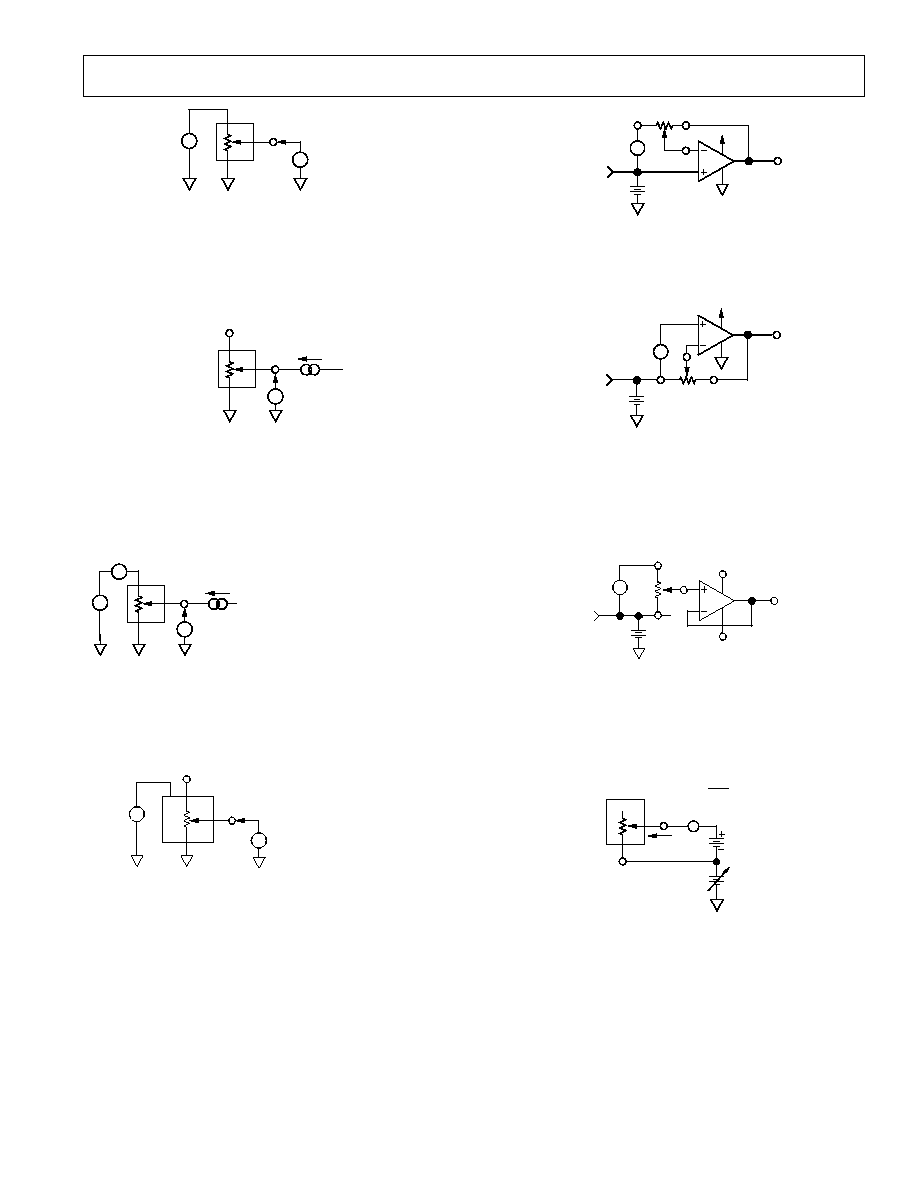
Parametric Test Circuits≠AD8400/AD8402/AD8403
V+
DUT
V
MS
A
B
W
V+ = V
DD
1LSB = V+/256
Figure 29. Potentiometer Divider Nonlinearity Error Test
Circuit (INL, DNL)
DUT
V
MS
A
B
W
NO CONNECT
I
W
Figure 30. Resistor Position Nonlinearity Error (Rheostat
Operation; R-INL, R-DNL)
I
MS
V
W2
≠ [V
W1
+ I
W
(R
AW
II R
BW
)]
I
W
V+
V
DD
WHERE V
W1
= V
MS
WHEN
I
W
= 0
AND V
W2
= V
MS
WHEN
I
W
= 1/R
V+
DUT
V
MS
A
B
W
V
W
I
W
=
1V/R
NOMINAL
R
W
= ≠≠≠≠≠≠≠≠≠≠≠≠≠≠≠≠≠≠≠≠≠≠≠≠≠≠
Figure 31. Wiper Resistance Test Circuit
PSRR (dB) = 20LOG
(
≠≠≠≠≠
)
PSS (%/%) = ≠≠≠≠≠≠≠
V
MS
V
DD
V
MS
%
V
DD
%
V+ = V
DD
±
10%
V+
V
MS
A
B
W
V
DD
V
A
~
Figure 32. Power Supply Sensitivity Test Circuit (PSS,
PSRR)
A
B
V
IN
2.5V DC
OP279
+5V
V
OUT
~
DUT
W
OFFSET
GND
Figure 33. Inverting Programmable Gain Test Circuit
~
A
B
V
IN
2.5V
OP279
+5V
V
OUT
DUT
W
OFFSET
GND
Figure 34. Noninverting Programmable Gain Test Circuit
~
B
A
V
IN
2.5V
+15V
V
OUT
DUT
W
≠15V
OFFSET
GND
OP42
Figure 35. Gain vs. Frequency Test Circuit
DUT
I
SW
B
W
0 toV
DD
R
SW
=
0.1V
I
SW
CODE = ÿÿ
H
0.1V
Figure 36. Incremental ON Resistance Test Circuit
REV. B
≠11≠

AD8400/AD8402/AD8403
≠12≠
REV. B
PROGRAMMING THE VARIABLE RESISTOR
Rheostat Operation
The nominal resistance of the VR (RDAC) between terminals A
and B are available with values of 1 k
, 10 k
, 50 k
and 100 k
.
The final digits of the part number determine the nominal resis-
tance value, e.g., 10 k
= 10; 100 k
= 100. The nominal resis-
tance (R
AB
) of the VR has 256 contact points accessed by the
wiper terminal, plus the B terminal contact. The 8-bit data word
in the RDAC latch is decoded to select one of the 256 possible
settings. The wiper's first connection starts at the B terminal for
data 00
H
. This B terminal connection has a wiper contact resis-
tance of 50
. The second connection (10 k
part) is the first
tap point located at 89
[= R
BA
(nominal resistance)/256 + R
W
= 39
+ 50
] for data 01
H
. The third connection is the next
tap point representing 78 + 50 = 128
for data 02
H
. Each LSB
data value increase moves the wiper up the resistor ladder until
the last tap point is reached at 10011
. The wiper does not di-
rectly connect to the B terminal. See Figure 37 for a simplified
diagram of the equivalent RDAC circuit.
The AD8400 contains one RDAC, the AD8402 contains two
independent RDACs and the AD8403 contains four independent
RDACs. The general transfer equation that determines the digi-
tally programmed output resistance between Wx and Bx is:
R
WB
(Dx) = (Dx)/256
◊
R
BA
+ R
W
Equation 2
where Dx is the data contained in the 8-bit RDAC# latch, and
R
BA
is the nominal end-to-end resistance.
For example, when V
B
= 0 V and A terminal is open circuit, the
following output resistance values will be set for the following
RDAC latch codes (applies to 10 k
potentiometers):
D
R
WB
(Dec)
(
)
Output State
255
10011
Full Scale
128
5050
Midscale (RS = 0 Condition)
1
89
1 LSB
0
50
Zero-Scale (Wiper Contact Resistance)
Note in the zero-scale condition a finite wiper resistance of 50
is present. Care should be taken to limit the current flow be-
tween W and B in this state to a maximum value of 5 mA to
avoid degradation or possible destruction of the internal switch
contact.
Like the mechanical potentiometer the RDAC replaces, it is to-
tally symmetrical. The resistance between the wiper W and ter-
minal A also produces a digitally controlled resistance R
WA
.
When these terminals are used the B terminal should be tied to
the wiper. Setting the resistance value for R
WA
starts at a maxi-
mum value of resistance and decreases as the data loaded in the
RDAC latch is increased in value. The general transfer equation
for this operation is:
R
WA
(Dx) = (256≠Dx)/256
◊
R
BA
+ R
W
Equation 3
OPERATION
The AD8400/AD8402/AD8403 provide a single, dual and quad
channel, 256 position digitally controlled variable resistor (VR)
device. Changing the programmed VR settings is accomplished
by clocking in a 10-bit serial data word into the SDI (Serial
Data Input) pin. The format of this data word is two address
bits, MSB first, followed by eight data bits, MSB first. Table I
provides the serial register data word format. The AD8400/
AD8402/AD8403 has the following address assignments for the
ADDR decode, which determines the location of VR latch re-
ceiving the serial register data in Bits B7 through B0:
VR# = A1
◊
2 + A0 + 1
Equation 1
The single-channel AD8400 requires A1 = A0 = 0. The dual-
channel AD8402 requires A1 = 0. VR settings can be changed
one at a time in random sequence. The serial clock running at
10 MHz makes it possible to load all 4 VRs in under 4
µ
s (10
◊
4
◊
100 ns) for the AD8403. The exact timing requirements are
shown in Figures 1a, 1b and 1c.
The AD8402/AD8403 resets to midscale by asserting the RS
pin, simplifying initial conditions at power up. Both parts have a
power shutdown SHDN pin that places the VR in a zero power
consumption state where terminals Ax are open circuited and
the wiper Wx is connected to Bx resulting in only leakage cur-
rents being consumed in the VR structure. In shutdown mode
the VR latch settings are maintained so that returning to opera-
tional mode from power shutdown, the VR settings return to
their previous resistance values. The digital interface is still ac-
tive in shutdown, except that SDO is deactivated. Code changes
in the registers can be made that will produce new wiper posi-
tions when the device is taken out of shutdown.
D7
D6
D5
D4
D3
D2
D1
D0
RDAC
LATCH
&
DECODER
Ax
Wx
Bx
R
S
= R
NOMINAL
/256
R
S
R
S
R
S
R
S
SHDN
Figure 37. AD8402/AD8403 Equivalent VR (RDAC) Circuit
AD8400/AD8402/AD8403
REV. B
≠13≠
where Dx is the data contained in the 8-bit RDAC# latch, and
R
BA
is the nominal end-to-end resistance. For example, when
V
A
= 0 V and B terminal is open circuit, the following output
resistance values will be set for the following RDAC latch codes
(applies to 10 k
potentiometers):
D
R
WA
(Dec)
(
)
Output State
255
89
Full Scale
128
5050
Midscale (RS = 0 Condition)
1
10011
1 LSB
0
10050
Zero Scale
The typical distribution of R
BA
from channel-to-channel matches
within
±
1%. However, device-to-device matching is process lot
dependent having a
±
20% variation. The change in R
BA
with
temperature has a positive 500 ppm/
∞
C temperature coefficient.
The wiper-to-end-terminal resistance temperature coefficient
has the best performance over the 10% to 100% of adjustment
range where the internal wiper contact switches do not contribute
any significant temperature related errors. The graph in Figure
11 shows the performance of R
WB
tempco vs. code, using the
trimmer with codes below 32 results in the larger temperature
coefficients plotted.
PROGRAMMING THE POTENTIOMETER DIVIDER
Voltage Output Operation
The digital potentiometer easily generates an output voltage
proportional to the input voltage applied to a given terminal.
For example, connecting A terminal to +5 V and B terminal to
ground produces an output voltage at the wiper starting at zero
volts up to 1 LSB less than +5 V. Each LSB of voltage is equal
to the voltage applied across terminal AB divided by the 256
position resolution of the potentiometer divider. The general
equation defining the output voltage with respect to ground for
any given input voltage applied to terminals AB is:
V
W
(Dx) = Dx/256
◊
V
AB
+ V
B
Equation 4
Operation of the digital potentiometer in the divider mode re-
sults in more accurate operation over temperature. Here the
output voltage is dependent on the ratio of the internal resistors,
not the absolute value; therefore, the temperature drift improves
to 15 ppm/
∞
C.
At the lower wiper position settings, the potentiometer divider
temperature coefficient increases due to the contributions of the
CMOS switch wiper resistance becoming an appreciable portion
of the total resistance from terminal B to the wiper. See Figure 10
for a plot of potentiometer tempco performance versus code
setting.
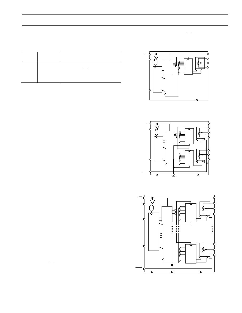
DIGITAL INTERFACING
The AD8400/AD8402/AD8403 contains a standard SPI com-
patible three-wire serial input control interface. The three inputs
are clock (CLK), CS and serial data input (SDI). The positive-
edge sensitive CLK input requires clean transitions to avoid
clocking incorrect data into the serial input register. For best re-
sults use logic transitions faster than 1 V/
µ
s. Standard logic
families work well. If mechanical switches are used for product
evaluation, they should be debounced by a flip-flop or other
suitable means. The Figure 38 block diagrams show more detail
of the internal digital circuitry. When CS is taken active low, the
clock loads data into the 10-bit serial register on each positive
clock edge (see Table II).
R
DAC
LAT
#1
GND
A1
W1
B1
V
DD
AD8400
CS
CLK
8
D7
D0
EN
ADDR
DEC
A1
A0
SDI
DI
SER
REG
D0
D7
10-BIT
a.
R
DAC
LAT
#1
R
AGND
RS
A1
W1
B1
V
DD
AD8402
CS
CLK
8
D7
D0
R
DAC
LAT
#2
R
A4
W4
B4
D7
D0
EN
ADDR
DEC
A1
A0
SDI
DI
10-BIT
SER
REG
D0
SHDN
DGND
D7
b.
R
DAC
LAT
#1
R
AGND
RS
A1
W1
B1
V
DD
AD8403
CS
CLK
SDO
8
D7
D0
R
DAC
LAT
#4
R
A4
W4
B4
D7
D0
EN
ADDR
DEC
A1
A0
D7
SDI
DO
DI
SER
REG
D0
SHDN
DGND
c.
Figure 38. Block Diagrams

AD8400/AD8402/AD8403
≠14≠
REV. B
Table II. Input Logic Control Truth Table
CLK CS
RS
SHDN
Register Activity
L
L
H
H
No SR effect, enables SDO pin.
P
L
H
H
Shift One bit in from the SDI pin.
The tenth previously entered bit is
shifted out of the SDO pin.
X
P
H
H
Load SR data into RDAC latch
based on A1, A0 decode (Table III).
X
H
H
H
No Operation.
X
X
L
H
Sets all RDAC latches to midscale,
wiper centered, and SDO latch
cleared.
X
H
P
H
Latches all RDAC latches to 80
H
.
X
H
H
L
Open circuits all resistor
A≠terminals, connects W to B,
turns off SDO output transistor.
NOTE: P = positive edge, X = don't care, SR = shift register.
The serial data-output (SDO) pin contains an open drain n-
channel FET. This output requires a pull-up resistor in order to
transfer data to the next package's SDI pin. The pull-up resistor
termination voltage may be larger than the V
DD
supply (but less
than max V
DD
of +8 V) of the AD8403 SDO output device,
e.g., the AD8403 could operate at V
DD
= 3.3 V and the pull-up
for interface to the next device could be set at +5 V. This allows
for daisy chaining several RDACs from a single processor serial
data line. The clock period needs to be increased when using a
pull-up resistor to the SDI pin of the following device in the
series. Capacitive loading at the daisy chain node SDO≠SDI
between devices must be accounted for to successfully transfer
data. When daisy chaining is used, the CS should be kept low
until all the bits of every package are clocked into their respec-
tive serial registers insuring that the address bits and data bits
are in the proper decoding location. This would require 20 bits
of address and data complying to the word format provided in
Table I if two AD8403 four-channel RDACs are daisy chained.
Note, only the AD8403 has a SDO pin. During shutdown
SHDN
the SDO output pin is forced to the off (logic high state)
to disable power dissipation in the pull up resistor. See Figure 40
for equivalent SDO output circuit schematic.
The data setup and data hold times in the specification table de-
termine the data valid time requirements. The last 10 bits of the
data word entered into the serial register are held when CS re-
turns high. At the same time CS goes high it gates the address
decoder, which enables one of the two (AD8402) or four
(AD8403) positive edge triggered RDAC latches. See Figure 39
detail and Table III Address Decode Table.
Table III. Address Decode Table
A1
A0
Latch Decoded
0
0
RDAC#1
0
1
RDAC#2
1
0
RDAC#3 AD8403 Only
1
1
RDAC#4 AD8403 Only
ADDR
DECODE
RDAC 1
RDAC 2
RDAC 4
SERIAL
REGISTER
AD8403
SDI
CLK
CS
Figure 39. Equivalent Input Control Logic
The target RDAC latch is loaded with the last eight bits of the
serial data word completing one DAC update. In the case of the
AD8403 four separate 10-bit data words must be clocked in to
change all four VR settings.
SERIAL
REGISTER
SDI
CK
RS
D
Q
SHDN
CS
CLK
RS
SDO
Figure 40. Detail SDO Output Schematic of the AD8403
All digital pins are protected with a series input resistor and par-
allel Zener ESD structure shown in Figure 41a. This structure
applies to digital pins CS, SDI, SDO, RS, SHDN, CLK. The
digital input ESD protection allows for mixed power supply
applications where +5 V CMOS logic can be used to drive an
AD8400/AD8402 or AD8403 operating from a +3 V power sup-
ply. The analog pins A, B, W are protected with a 20
series
resistor and parallel Zener, see Figure 41b.
1k
DIGITAL
PINS
LOGIC
Figure 41a. Equivalent ESD Protection Circuits
20
A, B, W
Figure 41b. Equivalent ESD Protection Circuit (Analog
Pins)
C
W
120pF
A
B
C
A
C
B
W
C
A
= 90.4pF ∑ ( ) + 30pF
DW
256
RDAC
10k
C
B
= 90.4pF ∑ (1 ≠ ) + 30pF
DW
256
Figure 42. RDAC Circuit Simulation Model for RDAC =
10 k

AD8400/AD8402/AD8403
REV. B
≠15≠
The ac characteristics of the RDACs are dominated by the inter-
nal parasitic capacitances and the external capacitive loads. The
≠3 dB bandwidth of the AD8403AN10 (10 k
resistor) mea-
sures 600 kHz at half scale as a potentiometer divider. Figure 23
provides the large signal BODE plot characteristics of the three
available resistor versions 10 k
, 50 k
, and 100 k
. The gain
flatness versus frequency graph, Figure 26, predicts filter appli-
cations performance. A parasitic simulation model has been de-
veloped, and is shown in Figure 42. Listing I provides a macro
model net list for the 10 k
RDAC:
Listing I. Macro Model Net List for RDAC
.PARAM DW=255, RDAC=10E3
*
.SUBCKT DPOT (A,W,)
*
CA
A
0
{DW/256*90.4E-12+30E-12}
RAW
A
W
{(1-DW/256)*RDAC+50}
CW
W
0
120E-12
RBW
W
B
{DW/256*RDAC+50}
CB
B
0
{(1-DW/256)*90.4E-12+30E-12}
*
.ENDS DPOT
The total harmonic distortion plus noise (THD+N) is measured
at 0.003% in an inverting op amp circuit using an offset ground
and a rail-to-rail OP279 amplifier, Figure 33. Thermal noise is
primarily Johnson noise, typically 9 nV/
Hz
for the 10 k
ver-
sion at f = 1 kHz. For the 100 k
device, thermal noise becomes
29 nV/
Hz
. Channel-to-channel crosstalk measures less than
≠65 dB at f = 100 kHz. To achieve this isolation, the extra ground
pins provided on the package to segregate the individual RDACs
must be connected to circuit ground. AGND and DGND pins
should be at the same voltage potential. Any unused potentio-
meters in a package should be connected to ground. Power sup-
ply rejection is typically ≠35 dB at 10 kHz (care is needed to
minimize power supply ripple in high accuracy applications).
APPLICATIONS
The digital potentiometer (RDAC) allows many of the applica-
tions of trimming potentiometers to be replaced by a solid-state
solution offering compact size, freedom from vibration, shock
and open contact problems encountered in hostile environ-
ments. A major advantage of the digital potentiometer is its
programmability. Any settings can be saved for later recall in
system memory.
The two major configurations of the RDAC include the
potentiometer divider (basic 3-terminal application) and the
rheostat (2-terminal configuration) connections shown in
Figures 29 and 30.
Certain boundary conditions must be satisfied for proper
AD8400/AD8402/AD8403 operation. First, all analog signals
must remain within the 0 to V
DD
range used to operate the
single-supply AD8400/AD8402/AD8403 products. For standard
potentiometer divider applications, the wiper output can be
used directly. For low resistance loads, buffer the wiper with a
suitable rail-to-rail op amp such as the OP291 or the OP279.
Second, for ac signals and bipolar dc adjustment applications, a
virtual ground will generally be needed. Whatever method is
used to create the virtual ground, the result must provide the
necessary sink and source current for all connected loads, in-
cluding adequate bypass capacitance. Figure 33 shows one
channel of the AD8402 connected in an inverting program-
mable gain amplifier circuit. The virtual ground is set at +2.5 V
which allows the circuit output to span a
±
2.5 volt range with
respect to virtual ground. The rail-to-rail amplifier capability is
necessary for the widest output swing. As the wiper is adjusted
from its midscale reset position (80
H
) toward the A terminal
(code FF
H
), the voltage gain of the circuit is increased in suc-
cessfully larger increments. Alternatively, as the wiper is ad-
justed toward the B terminal (code 00
H
), the signal becomes
attenuated. The plot in Figure 43 shows the wiper settings for a
100:1 range of voltage gain (V/V). Note the
±
10 dB of pseudo-
logarithmic gain around 0 dB (1 V/V). This circuit is mainly
useful for gain adjustments in the range of 0.14 V/V to 4 V/V;
beyond this range the step sizes become very large and the resis-
tance of the driving circuit can become a significant term in the
gain equation.
INVERTING GAIN ≠ V/V
256
128
0
0.1
1.0
10
96
64
32
160
192
224
DIGITAL CODE ≠ Decimal
Figure 43. Inverting Programmable Gain Plot
AD8400/AD8402/AD8403
≠16≠
REV. B
ACTIVE FILTER
One of the standard circuits used to generate a low-pass, high-
pass or bandpass filter is the state variable active filter. The digi-
tal potentiometer allows full programmability of the frequency,
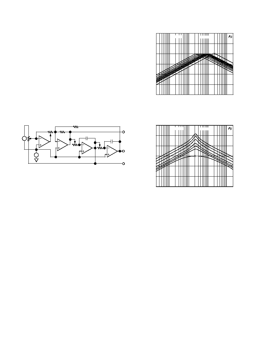
gain and Q of the filter outputs. Figure 44 shows the filter cir-
cuit using a +2.5 V virtual ground, which allows a
±
2.5 V
P
input
and output swing. RDAC2 and 3 set the LP, HP and BP cutoff
and center frequencies respectively. These variable resistors
should be programmed with the same data (as with ganged po-
tentiometers) to maintain the best circuit Q. Figure 45 shows
the measured filter response at the bandpass output as a func-
tion of the RDAC2 and RDAC3 settings which produce a range
of center frequencies from 2 kHz to 20 kHz. The filter gain re-
sponse at the bandpass output is shown in Figure 46. At a cen-
ter frequency of 2 kHz, the gain is adjusted over a ≠20 dB to
+20 dB range determined by RDAC1. Circuit Q is adjusted by
RDAC4. For more detailed reading on the state variable active
filter, see Analog Devices' application note, AN-318.
A1
A2
A3
A4
~
10k
RDAC4
10k
RDAC2
RDAC3
0.01µF
2.5V
0.01µF
RDAC1
V
IN
OP279
◊
2
HIGH-
PASS
LOW-
PASS
BAND-
PASS
±
B
B
B
B
Figure 44. Programmable State Variable Active Filter
FREQUENCY ≠ Hz
40
20
≠80
20
100k
100
1k
10k
0
≠20
≠40
≠60
200k
AMPLITUDE ≠ dB
≠0.16
20.0000 k
Figure 45. Programmed Center Frequency Bandpass
Response
FREQUENCY ≠ Hz
40
20
≠80
20
100k
100
1k
10k
0
≠20
≠40
≠60
200k
AMPLITUDE ≠ dB
≠19.01
2.00000 k
Figure 46. Programmed Amplitude Bandpass Response
AD8400/AD8402/AD8403
REV. B
≠17≠
OUTLINE DIMENSIONS
Dimensions shown in inches and (mm)
8-Pin Plastic DIP (N-8)
8
1
4
5
0.430 (10.92)
0.348 (8.84)
0.280 (7.11)
0.240 (6.10)
PIN 1
SEATING
PLANE
0.022 (0.558)
0.014 (0.356)
0.060 (1.52)
0.015 (0.38)
0.210 (5.33)
MAX
0.130
(3.30)
MIN
0.070 (1.77)
0.045 (1.15)
0.100
(2.54)
BSC
0.160 (4.06)
0.115 (2.93)
0.325 (8.25)
0.300 (7.62)
0.015 (0.381)
0.008 (0.204)
0.195 (4.95)
0.115 (2.93)
8-Lead SOIC (SO-8)
0.1968 (5.00)
0.1890 (4.80)
8
5
4
1
0.2440 (6.20)
0.2284 (5.80)
PIN 1
0.1574 (4.00)
0.1497 (3.80)
0.0688 (1.75)
0.0532 (1.35)
SEATING
PLANE
0.0098 (0.25)
0.0040 (0.10)
0.0192 (0.49)
0.0138 (0.35)
0.0500
(1.27)
BSC
0.0098 (0.25)
0.0075 (0.19)
0.0500 (1.27)
0.0160 (0.41)
8
∞
0
∞
0.0196 (0.50)
0.0099 (0.25)
x 45
∞
14-Pin Plastic DIP Package (N-14)
0.210
(5.33)
MAX
0.160 (4.06)
0.115 (2.93)
0.795 (20.19)
0.725 (18.42)
0.022 (0.558)
0.014 (0.356)
0.100
(2.54)
BSC
0.070 (1.77)
0.045 (1.15)
SEATING
PLANE
0.060 (1.52)
0.015 (0.38)
0.130
(3.30)
MIN
PIN 1
0.280 (7.11)
0.240 (6.10)
7
8
14
1
0.325 (8.25)
0.300 (7.62)
0.015 (0.381)
0.008 (0.204)
0.195 (4.95)
0.115 (2.93)
14-Pin Narrow Body SOIC Package (SO-14)
0.0098 (0.25)
0.0075 (0.19)
0.0500 (1.27)
0.0160 (0.41)
8
∞
0
∞
0.0196 (0.50)
0.0099 (0.25)
x 45
∞
PIN 1
0.1574 (4.00)
0.1497 (3.80)
0.2440 (6.20)
0.2284 (5.80)
1
14
8
7
0.0192 (0.49)
0.0138 (0.35)
0.0500
(1.27)
BSC
0.0688 (1.75)
0.0532 (1.35)
0.3444 (8.75)
0.3367 (8.55)
0.0098 (0.25)
0.0040 (0.10)
14-Lead TSSOP
(RU-14)
14
8
7
1
0.201 (5.10)
0.193 (4.90)
0.256 (6.50)
0.246 (6.25)
0.177 (4.50)
0.169 (4.30)
PIN 1
SEATING
PLANE
0.006 (0.15)
0.002 (0.05)
0.0118 (0.30)
0.0075 (0.19)
0.0256
(0.65)
BSC
0.0433
(1.10)
MAX
0.0079 (0.20)
0.0035 (0.090)
0.028 (0.70)
0.020 (0.50)
8
∞
0
∞

AD8400/AD8402/AD8403
≠18≠
REV. B
24-Pin Narrow Body Plastic DIP Package (N-24)
0.325 (8.25)
0.300 (7.62)
0.015 (0.381)
0.008 (0.203)
0.195 (4.95)
0.115 (2.93)
PIN 1
0.280 (7.11)
0.240 (6.10)
24
1
13
12
0.210
(5.33)
MAX
0.022 (0.558)
0.014 (0.356)
0.100 (2.54)
BSC
0.070 (1.77)
0.045 (1.15)
SEATING
PLANE
0.130
(3.30)
MIN
1.275 (32.30)
1.125 (28.60)
0.015
(0.38)
MIN
0.160 (4.06)
0.115 (2.92)
24-Pin SOIC Package (SOL-24)
0.0125 (0.32)
0.0091 (0.23)
0.0500 (1.27)
0.0157 (0.40)
8
∞
0
∞
0.0291 (0.74)
0.0098 (0.25)
x 45
∞
PIN 1
0.2992 (7.60)
0.2914 (7.40)
0.4193 (10.65)
0.3937 (10.00)
13
12
1
24
0.0192 (0.49)
0.0138 (0.35)
0.0500
(1.27)
BSC
0.1043 (2.65)
0.0926 (2.35)
0.6141 (15.60)
0.5985 (15.20)
0.0118 (0.30)
0.0040 (0.10)
24-Lead Thin Surface Mount TSSOP Package (RU-24)
24
13
12
1
0.311 (7.90)
0.303 (7.70)
0.256 (6.50)
0.246 (6.25)
0.177 (4.50)
0.169 (4.30)
PIN 1
SEATING
PLANE
0.006 (0.15)
0.002 (0.05)
0.0118 (0.30)
0.0075 (0.19)
0.0256 (0.65)
BSC
0.0433
(1.10)
MAX
0.0079 (0.20)
0.0035 (0.090)
0.028 (0.70)
0.020 (0.50)
8
∞
0
∞

≠19≠

PRINTED IN U.S.A.
C1997b≠12≠1/97
≠20≠