 | ÐлекÑÑоннÑй компоненÑ: AD8509 | СкаÑаÑÑ:  PDF PDF  ZIP ZIP |
Äîêóìåíòàöèÿ è îïèñàíèÿ www.docs.chipfind.ru
9- and 11-Channel, Muxed Input
LCD Reference Buffers
AD8509/AD8511
Rev. B
Information furnished by Analog Devices is believed to be accurate and reliable.
However, no responsibility is assumed by Analog Devices for its use, nor for any
infringements of patents or other rights of third parties that may result from its use.
Specifications subject to change without notice. No license is granted by implication
or otherwise under any patent or patent rights of Analog Devices. Trademarks and
registered trademarks are the property of their respective owners.
One Technology Way, P.O. Box 9106, Norwood, MA 02062-9106, U.S.A.
Tel: 781.329.4700
www.analog.com
Fax: 781.326.8703
© 2005 Analog Devices, Inc. All rights reserved.
FEATURES
Single-supply operation: 3.3 V to 6.5 V
High output current: 300 mA
Low supply current: 6 mA
Stable with 1000 pF loads
Pin-compatible with LMC6009
Pin-compatible with CL-FP6131
48-lead, Pb-free, TSSOP package
APPLICATION
LCD line inversion gamma references
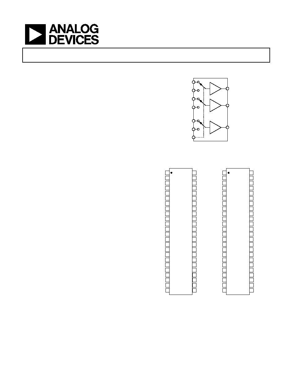
FUNCTIONAL BLOCK DIAGRAM
03237-001
INA1
INB1
INA2
INB2
INA11
INB11
A/B
VO11
VO2
VO1
Figure 1.
GENERAL DESCRIPTION
The AD8509 and AD8511 are 9-channel and 11-channel LCD
reference buffers, respectively, designed to drive 64 gray scale
column drivers. Each buffer has an A/B input to select between
two voltages for LCD displays. These buffers drive the resistor
ladders of LCD column drivers for gamma correction. These
LCD drivers have higher slew rates and higher output drive
currents than similar competitive parts. This increases the
stability of the reference ladder, resulting in better gray scale
and visual performance.
The AD8509 and AD8511 are specified over the -40°C to +85°C
temperature range. They are available in 48-lead, thin shrink
small outline (TSSOP), surface-mount, Pb-free packages in tape
and reel.
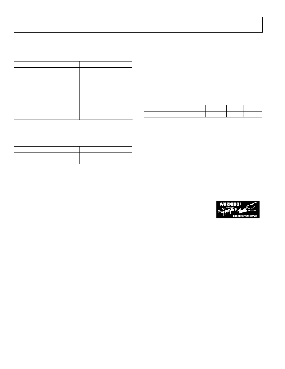
PIN CONFIGURATIONS
NC = NO CONNECT
14
13
12
11
10
9
8
1
2
3
4
7
6
5
19
18
17
16
15
20
23
22
21
24
29
28
27
32
31
30
40
39
38
37
36
35
34
33
26
25
41
42
43
44
45
46
47
48
NC
VO1
NC
NC
V
CC
GND
VO2
VO3
VO4
VO5
V
CC
GND
VO6
VO7
VO8
VO9
VO10
GND
V
CC
A/B
NC
INA1
INB1
INA2
INB2
INA3
INB3
INA4
INB4
INA5
INB5
INA6
INB6
INA7
INB7
INA8
INB8
INA9
INB9
INA10
NC
NC
VO11
NC
INB10
NC
INA11
INB11
AD8511
TOP VIEW
(Not to Scale)
NC = NO CONNECT
14
13
12
11
10
9
8
1
2
3
4
7
6
5
19
18
17
16
15
20
23
22
21
24
29
28
27
32
31
30
40
39
38
37
36
35
34
33
26
25
41
42
43
44
45
46
47
48
NC
NC
NC
NC
V
CC
GND
VO1
VO2
VO3
VO4
V
CC
GND
VO5
VO6
VO7
VO8
VO9
GND
V
CC
A/B
NC
NC
NC
INA1
INB1
INA2
INB2
INA3
INB3
INA4
INB4
INA5
INB5
INA6
INB6
INA7
INB7
INA8
INB8
INA9
NC
NC
NC
NC
INB9
NC
NC
NC
AD8509
TOP VIEW
(Not to Scale)
03237-002
Figure 2. AD8509 and AD8511 48-Lead TSSOP (RU Suffix)

AD8509/AD8511
Rev. B | Page 2 of 8
TABLE OF CONTENTS
Specifications..................................................................................... 3
Electrical Characteristics............................................................. 3
Absolute Maximum Ratings............................................................ 4
ESD Caution.................................................................................. 4
Typical Performance Characteristics ............................................. 5
Applications....................................................................................... 7
Outline Dimensions ......................................................................... 8
Ordering Guide............................................................................. 8
REVISION HISTORY
1/05--Rev. A to Rev. B
Changed Maximum Operating Voltage...........................Universal
Change to Features List.................................................................... 1
Changes to Specifications Table...................................................... 3
Changes to Ordering Guide ............................................................ 8
9/04--Rev. 0 to Rev. A
Format Updated..................................................................Universal
Added Pb-Free Part............................................................Universal
Changed Temperature Range............................................Universal
Changed Applications Section........................................................ 1
Changes to Ordering Guide ............................................................ 8
10/97--Revision 0: Initial Version

AD8509/AD8511
Rev. B | Page 3 of 8
SPECIFICATIONS
ELECTRICAL CHARACTERISTICS
V
S
= 5 V, T
A
= 25°C, unless otherwise noted.
Table 1.
Parameter
Symbol
Conditions
Min
Typ
Max
Unit
INPUT CHARACTERISTICS
Offset Voltage
V
OS
20
mV
Input Bias Current
I
B
50
nA
Voltage Gain
A
VO
0.985
V/V
OUTPUT CHARACTERISTICS
Output Voltage High
V
OH
I
LOAD
= +20 mA
4.8
V
Output Voltage Low
V
OL
I
LOAD
= -20 mA
200
mV
Output Short-Circuit Current
I
SC
120
350
mA
POWER SUPPLY
Load Regulation
V
IN
= 0.5 V - 4.5 V, I
SOURCE
= 20 mA
7
mV
V
IN
= 0.5 V - 4.5 V, I
SINK
= 20 mA
7
mV
Supply Current
I
SY
AD8509, V
IN
= 2.5 V
8.5
mA
I
SY
AD8511, V
IN
= 2.5 V
10
mA
Supply Voltage Range
V
S
3.3
6.5
V
DYNAMIC PERFORMANCE
Slew Rate
C
L
= 15 pF
7
V/µs
R
L
= 250
6.2
V/µs
Settling Time
t
S
IDC = 13 mA (sink/source)
3
6
µs
LOGIC INPUT CHARACTERISTICS
Input Current Low
I
IL
1.0
µA
Input Current High
I
IH
1.5
µA
Input Voltage Low
V
IL
0.8
V
Input Voltage High
V
IH
2.0
V
AD8509/AD8511
Rev. B | Page 4 of 8
ABSOLUTE MAXIMUM RATINGS
Table 2.
Parameter Rating
Supply Voltage
7 V
Input Voltage
GND to V
S
Storage Temperature Range
RU Package
-65°C to +150°C
Operating Temperature Range
-40°C to +85°C
Junction Temperature Range
RU Package
-65°C to +150°C
Lead Temperature Range
(Soldering, 60 sec)
300°C
Stresses above those listed under Absolute Maximum Ratings
may cause permanent damage to the device. This is a stress
rating only; the functional operation of the device at these or
any other conditions above those indicated in the operational
sections of this specification is not implied. Exposure to
absolute maximum rating conditions for extended periods may
affect device reliability.
Table 3.
Package Type
JA
1
JC
Unit
48-lead Pb-free TSSOP (RU)
115
42
°C/W
1
JA
is specified for the worst-case conditions, that is,
JA
is specified for
devices soldered in circuit boards for surface-mount packages.
Table 4. MUX Function
A/B Select (Pin 29)
Input
Logic High
INAx
Logic Low
INBx
ESD CAUTION
ESD (electrostatic discharge) sensitive device. Electrostatic charges as high as 4000 V readily accumulate on
the human body and test equipment and can discharge without detection. Although this product features
proprietary ESD protection circuitry, permanent damage may occur on devices subjected to high energy
electrostatic discharges. Therefore, proper ESD precautions are recommended to avoid performance
degradation or loss of functionality.
AD8509/AD8511
Rev. B | Page 5 of 8
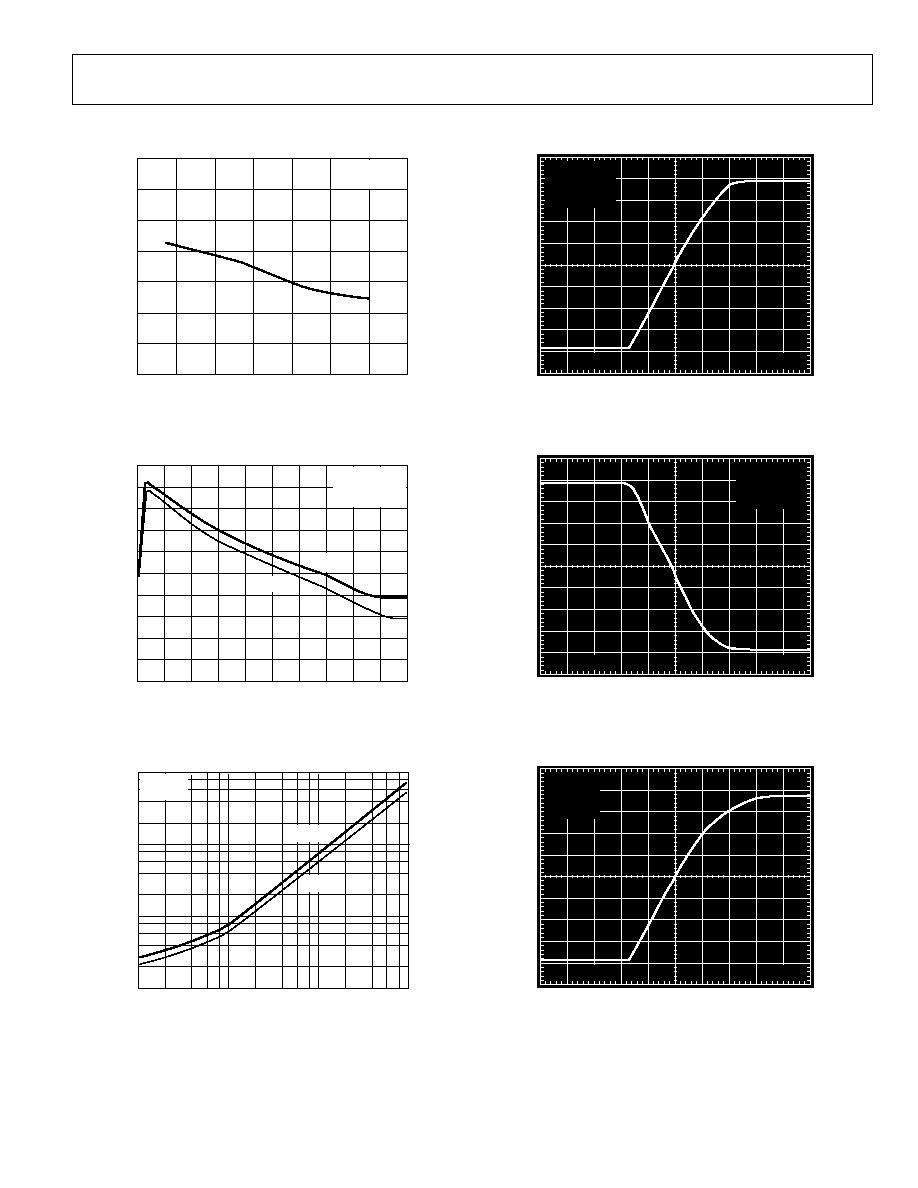
TYPICAL PERFORMANCE CHARACTERISTICS
10
9
8
7
6
5
4
3
35
15
5
25
45
65
85
105
03237-003
TEMPERATURE (
°
C)
SU
PPLY C
U
R
R
EN
T (
m
A
)
V
S
= 5V
R
L
= NO LOAD
Figure 3. Supply Current vs. Temperature
10
9
8
7
6
5
4
3
2
1
0
0
5
4
3
2
1
03237-004
COMMON-MODE VOLTAGE (V)
S
U
P
P
L
Y
CURRE
NT (mA)
AD8511
AD8509
V
S
= 5V
T
A
= 25
°
C
R
L
= NO LOAD
Figure 4. Supply Current vs. Common-Mode Voltage
1k
100
10
1
0.1
100
10
1
03237-005
LOAD CURRENT (mA)
OUTPUT VOLTAGE (mV)
SOURCE
SINK
V
S
= 5V
T
A
= 25
°
C
Figure 5. Output Voltage to Supply Rail vs. Load Current
03237-006
V
S
= 5V
T
A
= 25
°
C
R
L
= NO LOAD
C
L
= 15pF
620mV
2.5V
Figure 6. Large Signal Transient Response--Rising
03237-007
V
S
= 5V
T
A
= 25
°
C
R
L
= NO LOAD
C
L
= 15pF
620mV
2.5V
Figure 7. Large Signal Transient Response--Falling
03237-008
V
S
= 5V
T
A
= 25
°
C
R
L
= 250
C
L
= 15pF
620mV
2.5V
Figure 8. Large Signal Transient Response--Rising
Document Outline
- FEATURES
- APPLICATION
- GENERAL DESCRIPTION
- FUNCTIONAL BLOCK DIAGRAM
- PIN CONFIGURATIONS
- þÿ
- þÿ
- þÿ
- þÿ
- þÿ