 | –≠–ª–µ–∫—Ç—Ä–æ–Ω–Ω—ã–π –∫–æ–º–ø–æ–Ω–µ–Ω—Ç: AD8531 | –°–∫–∞—á–∞—Ç—å:  PDF PDF  ZIP ZIP |
Document Outline
- FEATURES
- APPLICATIONS
- GENERAL DESCRIPTION
- PIN CONFIGURATIONS
- SPECIFICATIONS
- ABSOLUTE MAXIMUM RATINGS
- PACKAGE INFORMATION
- ORDERING GUIDE
- Typical Performance Characteristics
- APPLICATIONS
- THEORY OF OPERATION
- Short-Circuit Protection
- Power Dissipation
- Calculating Power by Measuring Ambient and Case Temperature
- Calculating Power by Measuring Supply Current
- Input Overvoltage Protection
- Output Phase Reversal
- Capacitive Load Drive
- A High Output Current, Buffered Reference/Regulator
- A Single-Supply, Balanced Line Driver
- A Single-Supply Headphone Amplifier
- A Single-Supply, Two-Way Loudspeaker Crossover Network
- Direct Access Arrangement for Telephone Line Interface
- OUTLINE DIMENSIONS
- Revision History

REV. D
Information furnished by Analog Devices is believed to be accurate and
reliable. However, no responsibility is assumed by Analog Devices for its
use, nor for any infringements of patents or other rights of third parties that
may result from its use. No license is granted by implication or otherwise
under any patent or patent rights of Analog Devices.
a
Low Cost, 250 mA Output
Single-Supply Amplifiers
AD8531/AD8532/AD8534
GENERAL DESCRIPTION
The AD8531, AD8532, and AD8534 are single, dual and quad
rail-to-rail input and output single-supply amplifiers featuring
250 mA output drive current. This high output current makes
these amplifiers excellent for driving either resistive or capacitive
loads. AC performance is very good with 3 MHz bandwidth,
5 V/
ms slew rate and low distortion. All are guaranteed to oper-
ate from a 3 volt single supply as well as a 5 volt supply.
The very low input bias currents enable the AD853x to be used
for integrators, diode amplification and other applications requiring
low input bias current. Supply current is only 750
mA per amplifier
at 5 volts, allowing low current applications to control high
current loads.
Applications include audio amplification for computers, sound
ports, sound cards and set-top boxes. The AD853x family is
very stable and capable of driving heavy capacitive loads, such as
those found in LCDs.
The ability to swing rail-to-rail at the inputs and outputs enables
designers to buffer CMOS DACs, ASICs or other wide output
swing devices in single-supply systems.
The AD8531, AD8532, and AD8534 are specified over the
extended industrial (≠40
C to +85C) temperature range. The
AD8531. The AD8532 is available in 8-lead SOIC, MSOP,
TSSOP surface-mount packages. The AD8534 is available in
narrow SO-14 and 14-lead TSSOP surface-mount packages.
All TSSOP, SOT, and SC70 versions are available in tape
and reel only.
FEATURES
Single-Supply Operation: 2.7 Volts to 6 Volts
High Output Current: 250 mA
Low Supply Current: 750 A/Amplifier
Wide Bandwidth: 3 MHz
Slew Rate: 5 V/ s
No Phase Reversal
Low Input Currents
Unity Gain Stable
Rail-to-Rail Input and Output
APPLICATIONS
Multimedia Audio
LCD Driver
ASIC Input or Output Amplifier
Headphone Driver
PIN CONFIGURATIONS
One Technology Way, P.O. Box 9106, Norwood, MA 02062-9106, U.S.A.
Tel: 781/329-4700
www.analog.com
Fax: 781/326-8703
© Analog Devices, Inc., 2002
14-Lead SOIC, and TSSOP
(R, and RU Suffixes)
AD8534
1
2
3
4
14
13
12
11
OUT A
≠IN A
+IN A
V+
V≠
+IN D
≠IN D
OUT D
5
6
7
10
9
8
+IN B
≠IN B
OUT B
OUT C
≠IN C
+IN C
8-Lead SOIC, TSSOP, and MSOP
(R, RU, and RM Suffixes)
AD8532
1
2
3
4
8
7
6
5
OUT A
≠IN A
+IN A
V≠
+IN B
≠IN B
OUT B
V+
8-Lead SOIC, TSSOP, and MSOP
(R, RU, and RM Suffixes)
NULL
≠IN A
+IN A
V≠
V+
OUT A
NULL
NC
1
2
3
4
8
7
6
5
AD8531
5-Lead SC70 and SOT-23
(KS and RT Suffixes)
1
2
3
5
4
IN A
+IN A
V+
OUT A
AD8531
V

REV. D
≠2≠
AD8531/AD8532/AD8534≠SPECIFICATIONS
ELECTRICAL CHARACTERISTICS
Parameter
Symbol
Conditions
Min
Typ
Max
Unit
INPUT CHARACTERISTICS
Offset Voltage
V
OS
25
mV
≠40
C £ T
A
£ +85C
30
mV
Input Bias Current
I
B
5
50
pA
≠40
C £ T
A
£ +85C
60
pA
Input Offset Current
I
OS
1
25
pA
≠40
C £ T
A
£ +85C
30
pA
Input Voltage Range
0
3
V
Common-Mode Rejection Ratio
CMRR
V
CM
= 0 V to 3 V
38
45
dB
Large Signal Voltage Gain
A
VO
R
L
= 2 k
W, V
O
= 0.5 V to 2.5 V
25
V/mV
Offset Voltage Drift
DV
OS
/
DT
20
mV/C
Bias Current Drift
DI
B
/
DT
50
fA/
C
Offset Current Drift
DI
OS
/
DT
20
fA/
C
OUTPUT CHARACTERISTICS
Output Voltage High
V
OH
I
L
= 10 mA
2.85
2.92
V
≠40
C £ T
A
£ +85C
2.8
V
Output Voltage Low
V
OL
I
L
= 10 mA
60
100
mV
≠40
C £ T
A
£ +85C
125
mV
Output Current
I
OUT
±250
mA
Closed-Loop Output Impedance
Z
OUT
f = 1 MHz, A
V
= 1
60
W
POWER SUPPLY
Power Supply Rejection Ratio
PSRR
V
S
= 3 V to 6 V
45
55
dB
Supply Current/Amplifier
I
SY
V
O
= 0 V
0.70
1
mA
≠40
C £ T
A
£ +85C
1.25
mA
DYNAMIC PERFORMANCE
Slew Rate
SR
R
L
= 2 k
W
3.5
V/
ms
Settling Time
t
S
To 0.01%
1.6
ms
Gain Bandwidth Product
GBP
2.2
MHz
Phase Margin
fo
70
Degrees
Channel Separation
CS
f = 1 kHz, R
L
= 2 k
W
65
dB
NOISE PERFORMANCE
Voltage Noise Density
e
n
f = 1 kHz
45
nV/
˜Hz
f = 10 kHz
30
nV/
˜Hz
Current Noise Density
i
n
f = 1 kHz
0.05
pA/
˜Hz
Specifications subject to change without notice.
(@ V
S
= 3.0 V, V
CM
= 1.5 V, T
A
= 25 C unless otherwise noted)

ELECTRICAL CHARACTERISTICS
Parameter
Symbol
Conditions
Min
Typ
Max
Unit
INPUT CHARACTERISTICS
Offset Voltage
V
OS
25
mV
≠40
C £ T
A
£ +85C
30
mV
Input Bias Current
I
B
5
50
pA
≠40
C £ T
A
£ +85C
60
pA
Input Offset Current
I
OS
1
25
pA
≠40
C £ T
A
£ +85C
30
pA
Input Voltage Range
0
5
V
Common-Mode Rejection Ratio
CMRR
V
CM
= 0 V to 5 V
38
47
dB
Large Signal Voltage Gain
A
VO
R
L
= 2 k
W, V
O
= 0.5 V to 4.5 V
15
80
V/mV
Offset Voltage Drift
DV
OS
/
DT
≠40
C £ T
A
£ +85C
20
mV/C
Bias Current Drift
DI
B
/
DT
50
fA/
C
Offset Current Drift
DI
OS
/
DT
20
fA/
C
OUTPUT CHARACTERISTICS
Output Voltage High
V
OH
I
L
= 10 mA
4.9
4.94
V
≠40
C £ T
A
£ +85C
4.85
V
Output Voltage Low
V
OL
I
L
= 10 mA
50
100
mV
≠40
C £ T
A
£ +85C
125
mV
Output Current
I
OUT
±250
mA
Closed-Loop Output Impedance
Z
OUT
f = 1 MHz, A
V
= 1
40
W
POWER SUPPLY
Power Supply Rejection Ratio
PSRR
V
S
= 3 V to 6 V
45
55
dB
Supply Current/Amplifier
I
SY
V
O
= 0 V
0.75
1.25
mA
≠40
C £ T
A
£ +85C
1.75
mA
DYNAMIC PERFORMANCE
Slew Rate
SR
R
L
= 2 k
W
5
V/
ms
Full-Power Bandwidth
BW
p
1% Distortion
350
kHz
Settling Time
t
S
To 0.01%
1.4
ms
Gain Bandwidth Product
GBP
3
MHz
Phase Margin
fo
70
Degrees
Channel Separation
CS
f = 1 kHz, R
L
= 2 k
W
65
dB
NOISE PERFORMANCE
Voltage Noise Density
e
n
f = 1 kHz
45
nV/
˜Hz
f = 10 kHz
30
nV/
˜Hz
Current Noise Density
i
n
f = 1 kHz
0.05
pA/
˜Hz
Specifications subject to change without notice.
AD8531/AD8532/AD8534
REV. D
≠3≠
(@ V
S
= 5.0 V, V
CM
= 2.5 V, T
A
= 25 C unless otherwise noted)

AD8531/AD8532/AD8534
REV. D
≠4≠
ABSOLUTE MAXIMUM RATINGS
1
Supply Voltage (V
S
) . . . . . . . . . . . . . . . . . . . . . . . . . . . . . . 7 V
Input Voltage . . . . . . . . . . . . . . . . . . . . . . . . . . . . . GND to V
S
Differential Input Voltage
2
. . . . . . . . . . . . . . . . . . . . . . .
±6 V
Storage Temperature Range . . . . . . . . . . . . ≠65
C to +150C
Operating Temperature Range . . . . . . . . . . . ≠40
C to +85C
Junction Temperature Range . . . . . . . . . . . . ≠65
C to +150C
Lead Temperature Range (Soldering, 60 sec) . . . . . . . . 300
C
NOTES
1
Stresses above those listed under Absolute Maximum Ratings may cause perma-
nent damage to the device. This is a stress rating only; the functional operation of
the device at these or any other conditions above those indicated in the operational
sections of this specification is not implied. Exposure to absolute maximum rating
conditions for extended periods may affect device reliability.
2
For supplies less than +6 volts, the differential input voltage is equal to
±V
S
.
2.5
2
1.5
1
0.5
0
0
20
40
60
80
100
120
140
160
180
200
R
LOAD
≠
V
OUT
+V
OH
≠V
OL
Figure 1. Output Voltage vs. Load. V
S
=
±2.5 V, R
L
Is Connected to GND (0 V)
PACKAGE INFORMATION
Package Type
JA
*
JC
Unit
5-Lead SC70 (KS)
376
126
C/W
5-Lead SOT-23 (RT)
230
146
C/W
8-Lead SOIC (RN)
158
43
C/W
8-Lead MSOP (RM)
210
45
C/W
8-Lead TSSOP (RU)
240
43
C/W
14-Lead SOIC (RN)
120
36
C/W
14-Lead TSSOP (RU)
240
43
C/W
*
q
JA
is specified for the worst case conditions, i.e.,
q
JA
is specified for device in socket
for P-DIP packages;
q
JA
is specified for device soldered onto a circuit board for
surface-mount packages.
ORDERING GUIDE
Model
Temperature Range
Package Description
Package Option
Branding Information
AD8531AKS
*
≠40
C to +85C
5-Lead SC70
KS-5
A7B
AD8531AR
≠40
C to +85C
8-Lead SOIC
RN-8
AD8531ART
*
≠40
C to +85C
5-Lead SOT-23
RT-5
A7A
AD8532AR
≠40
C to +85C
8-Lead SOIC
RN-8
AD8532ARM
*
≠40
C to +85C
8-Lead MSOP
RM-8
ARA
AD8532ARU
*
≠40
C to +85C
8-Lead TSSOP
RU-8
AD8534AR
≠40
C to +85C
14-Lead SOIC
RN-14
AD8534ARU
*
≠40
C to +85C
14-Lead TSSOP
RU-14
*Available in reels only.
CAUTION
ESD (electrostatic discharge) sensitive device. Electrostatic charges as high as 4000 V readily
accumulate on the human body and test equipment and can discharge without detection. Although
the AD8531/AD8532/AD8534 features proprietary ESD protection circuitry, permanent damage
may occur on devices subjected to high-energy electrostatic discharges. Therefore, proper ESD
precautions are recommended to avoid performance degradation or loss of functionality.
WARNING!
ESD SENSITIVE DEVICE
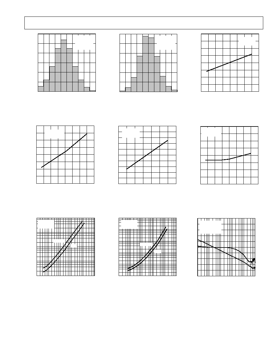
INPUT OFFSET VOLTAGE ≠ mV
QUANTITY ≠ Amplifiers
300
500
400
200
100
≠12 ≠10 ≠8 ≠6
≠4
≠2
0
2
4
V
S
= 2.7V
V
CM
= 1.35V
T
A
= 25 C
Figure 2. Input Offset Voltage
Distribution
TEMPERATURE ≠ C
≠35 ≠15
5
25
45
65
85
INPUT BIAS CURRENT ≠ pA
5
8
7
4
2
6
3
V
S
= 5V, 3V
V
CM
= V
S
/2
Figure 5. Input Bias Current vs.
Temperature
LOAD CURRENT ≠ mA
0.01
0.1
1000
1
10
100
OUTPUT VOLTAGE ≠ mV
1000
100
0.1
10
1
V
S
= 2.7V
T
A
= 25 C
SOURCE
SINK
Figure 8. Output Voltage to Supply
Rail vs. Load Current
Typical Performance Characteristics≠AD8531/AD8532/AD8534
REV. D
≠5≠
INPUT OFFSET VOLTAGE ≠ mV
QUANTITY ≠ Amplifiers
300
≠12 ≠10 ≠8
≠6
≠4 ≠2
0
2
4
500
400
200
100
V
S
= 5V
V
CM
= 2.5V
T
A
= 25 C
Figure 3. Input Offset Voltage
Distribution
COMMON-MODE VOLTAGE ≠ Volts
0
1
2
3
4
5
INPUT BIAS CURRENT ≠ pA
5
8
7
4
2
6
3
1
V
S
= 5V
T
A
= 25 C
Figure 6. Input Bias Current vs.
Common-Mode Voltage
LOAD CURRENT ≠ mA
0.01
0.1
1000
1
10
100
OUTPUT VOLTAGE ≠ mV
10000
100
0.01
10
1000
1
V
S
= 5V
T
A
= 25 C
SOURCE
SINK
Figure 9. Output Voltage to Supply
Rail vs. Load Current
TEMPERATURE ≠ C
≠35 ≠15
5
25
45
65
85
INPUT OFFSET VOLTAGE ≠ mV
≠5
≠2
≠3
≠6
≠8
≠4
≠7
V
S
= 5V
V
CM
= 2.5V
Figure 4. Input Offset Voltage
vs. Temperature
TEMPERATURE ≠ C
≠35
≠15
5
25
45
65
85
INPUT OFFSET CURRENT ≠ pA
3
2
0
4
1
≠1
≠2
5
6
V
S
= 5V, 3V
V
CM
= V
S
/2
Figure 7. Input Offset Current vs.
Temperature
FREQUENCY ≠ Hz
1k
10k
100k
1M
10M
100M
V
S
= 2.7V
R
L
= NO LOAD
T
A
= 25 C
80
60
40
20
0
GAIN ≠ dB
45
90
135
180
PHASE SHIFT ≠ De
g
rees
Figure 10. Open-Loop Gain and
Phase vs. Frequency