 | ÐлекÑÑоннÑй компоненÑ: AD8592 | СкаÑаÑÑ:  PDF PDF  ZIP ZIP |
Äîêóìåíòàöèÿ è îïèñàíèÿ www.docs.chipfind.ru
REV. A
Information furnished by Analog Devices is believed to be accurate and
reliable. However, no responsibility is assumed by Analog Devices for its
use, nor for any infringements of patents or other rights of third parties
which may result from its use. No license is granted by implication or
otherwise under any patent or patent rights of Analog Devices.
a
AD8591/AD8592/AD8594
One Technology Way, P.O. Box 9106, Norwood, MA 02062-9106, U.S.A.
Tel: 781/329-4700
World Wide Web Site: http://www.analog.com
Fax: 781/326-8703
© Analog Devices, Inc., 1999
CMOS Single Supply
Rail-to-Rail Input/Output
Operational Amplifiers with Shutdown
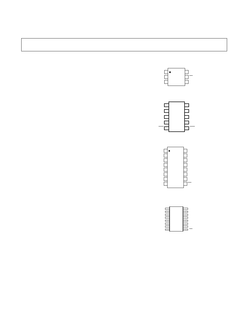
PIN CONFIGURATIONS
6-Lead SOT
(RT Suffix)
6
4
1
2
3
OUT A
IN A
V
V
IN A
5
SD
AD8591
10-Lead SOIC
(RM Suffix)
SDA
SDB
5
6
V
+IN B
4
7
OUT A
IN A
+IN A
V+
OUT B
1
2
3
10
9
8
IN B
AD8592
(Not to Scale)
16-Lead Narrow SOIC
(R Suffix)
TOP VIEW
(Not to Scale)
16
15
14
13
12
11
10
9
1
2
3
4
5
6
7
8
NC = NO CONNECT
OUT A
IN A
V
IN A
IN B
IN B
OUT B
NC
OUT D
IN D
IN D
V
IN C
IN C
OUT C
SD
AD8594
16-Lead TSSOP
(RU Suffix)
NC
SD
OUT A
IN A
IN A
V
IN D
IN D
V
OUT D
1
IN B
IN B
OUT B
IN C
OUT C
+IN C
16
AD8594
1
8
9
NC = NO CONNECT
FEATURES
Single Supply Operation: +2.5 V to +6 V
High Output Current: 250 mA
Extremely Low Shutdown Supply Current: 100 nA
Low Supply Current: 750 A/Amp
Wide Bandwidth: 3 MHz
Slew Rate: 5 V/ s
No Phase Reversal
Very Low Input Bias Current
High Impedance Outputs When in Shutdown Mode
Unity Gain Stable
APPLICATIONS
Mobile Communication Handset Audio
PC Audio
PCMCIA/Modem Line Driving
Battery Powered Instrumentation
Data Acquisition
ASIC Input or Output Amplifier
LCD Display Reference Level Driver
GENERAL DESCRIPTION
The AD8591, AD8592 and AD8594 are single, dual and quad
rail-to-rail input and output single supply amplifiers featuring
250 mA output drive current and a power saving shutdown
mode. The AD8592 includes an independent shutdown func-
tion for each amplifier. When both amplifiers are in shutdown
mode the total supply current is reduced to less than 1
µ
A. The
AD8591 and AD8594 include a single master shutdown func-
tion that reduces total supply current to less than 1
µ
A. All
amplifier outputs are in a high impedance state when in shut-
down mode.
These amplifiers have very low input bias currents, making them
suitable for integrators and diode amplification. Outputs are
stable with virtually any capacitive load. Supply current is less
than 750
µ
A per amplifier in active mode.
Applications for these amplifiers include audio amplification for
portable computers, portable phone headsets, sound ports, sound
cards and set-top boxes. The AD859x family is capable of driving
heavy capacitive loads such as LCD panel reference levels.
The ability to swing rail-to-rail at both the input and output
enables designers to buffer CMOS DACs, ASICs and other
wide output swing devices in single supply systems.
The AD8591, AD8592 and AD8594 are specified over the indus-
trial (40
°
C to +85
°
C) temperature range. The AD8591, single,
is available in the tiny 6-lead SOT package. The AD8592, dual, is
available in the 10-lead
µ
SOIC surface mount package. The
AD8594, quad, is available in 16-lead narrow SOIC and 16-lead
TSSOP packages.

2
REV. A
AD8591/AD8592/AD8594SPECIFICATIONS
ELECTRICAL CHARACTERISTICS
Parameter
Symbol
Conditions
Min
Typ
Max
Units
INPUT CHARACTERISTICS
Offset Voltage
V
OS
25
mV
40
°
C < T
A
< +85
°
C
30
mV
Input Bias Current
I
B
5
50
pA
40
°
C < T
A
< +85
°
C
60
pA
Input Offset Current
I
OS
1
25
pA
40
°
C < T
A
< +85
°
C
30
pA
Input Voltage Range
0
+2.7
V
Common-Mode Rejection Ratio
CMRR
V
CM
= 0 V to +2.7 V
38
45
dB
Large Signal Voltage Gain
A
VO
R
L
= 2 k
, V
O
= +0.3 V to +2.4 V
25
V/mV
Offset Voltage Drift
V
OS
/
T
20
µ
V/
°
C
Bias Current Drift
I
B
/
T
50
fA/
°
C
Offset Current Drift
I
OS
/
T
20
fA/
°
C
OUTPUT CHARACTERISTICS
Output Voltage High
V
OH
I
L
= 10 mA
+2.55
+2.61
V
40
°
C to +85
°
C
+2.5
V
Output Voltage Low
V
OL
I
L
= 10 mA
60
100
mV
40
°
C to +85
°
C
125
mV
Output Current
I
OUT
±
250
mA
Open-Loop Impedance
Z
OUT
f = 1 MHz, A
V
= 1
60
POWER SUPPLY
Power Supply Rejection Ratio
PSRR
V
S
= +2.5 V to +6 V
45
55
dB
Supply Current/Amplifier
I
SY
V
O
= 0 V
1
mA
40
°
C < T
A
< +85
°
C
1.25
mA
Supply Current Shutdown Mode
I
SD
All Amplifiers Shut Down
0.1
1
µ
A
40
°
C < T
A
< +85
°
C
1
µ
A
I
SD1
Amplifier 1 Shut Down (AD8592)
1.4
mA
I
SD2
Amplifier 2 Shut Down (AD8592)
1.4
mA
SHUTDOWN INPUTS
Logic High Voltage
V
INH
40
°
C < T
A
< +85
°
C
+1.6
V
Logic Low Voltage
V
INL
40
°
C < T
A
< +85
°
C
+0.5
V
Logic Input Current
I
IN
40
°
C < T
A
< +85
°
C
1
µ
A
DYNAMIC PERFORMANCE
Slew Rate
SR
R
L
= 2 k
3.5
V/
µ
s
Settling Time
t
S
To 0.01%
1.4
µ
s
Gain Bandwidth Product
GBP
2.2
MHz
Phase Margin
o
67
Degrees
Channel Separation
CS
f = 1 kHz, R
L
= 2 k
65
dB
NOISE PERFORMANCE
Voltage Noise Density
e
n
f = 1 kHz
45
nV/
Hz
f = 10 kHz
30
nV/
Hz
Current Noise Density
i
n
f = 1 kHz
0.05
pA/
Hz
Specifications subject to change without notice.
(V
S
= +2.7 V, V
CM
= +1.35 V, T
A
= +25 C unless otherwise noted)

3
REV. A
AD8591/AD8592/AD8594
ELECTRICAL CHARACTERISTICS
Parameter
Symbol
Conditions
Min
Typ
Max
Units
INPUT CHARACTERISTICS
Offset Voltage
V
OS
2
25
mV
40
°
C < T
A
< +85
°
C
30
mV
Input Bias Current
I
B
5
50
pA
40
°
C < T
A
< +85
°
C
60
pA
Input Offset Current
I
OS
1
25
pA
40
°
C < T
A
< +85
°
C
30
pA
Input Voltage Range
0
+5
V
Common-Mode Rejection Ratio
CMRR
V
CM
= 0 V to +5 V
38
47
dB
Large Signal Voltage Gain
A
VO
R
L
= 2 k
, V
O
= +0.5 V to +4.5 V
15
30
V/mV
Offset Voltage Drift
V
OS
/
T
40
°
C < T
A
< +85
°
C
20
µ
V/
°
C
Bias Current Drift
I
B
/
T
50
fA/
°
C
Offset Current Drift
I
OS
/
T
20
fA/
°
C
OUTPUT CHARACTERISTICS
Output Voltage High
V
OH
I
L
= 10 mA
+4.9
+4.94
V
40
°
C to +85
°
C
+4.85
V
Output Voltage Low
V
OL
I
L
= 10 mA
50
100
mV
40
°
C to +85
°
C
125
mV
Output Current
I
OUT
±
250
mA
Open-Loop Impedance
Z
OUT
f = 1 MHz, A
V
= 1
40
POWER SUPPLY
Power Supply Rejection Ratio
PSRR
V
S
= +2.5 V to +6 V
45
55
dB
Supply Current/Amplifier
I
SY
V
O
= 0 V
1.25
mA
40
°
C < T
A
< +85
°
C
1.75
mA
Supply Current-Shutdown Mode
I
SD
All Amplifiers Shut Down
0.1
1
µ
A
40
°
C < T
A
< +85
°
C
1
µ
A
I
SD1
Amplifier 1 Shut Down (AD8592)
1.6
mA
I
SD2
Amplifier 2 Shut Down (AD8592)
1.6
mA
SHUTDOWN INPUTS
Logic High Voltage
V
INH
40
°
C < T
A
< +85
°
C
+2.4
V
Logic Low Voltage
V
INL
40
°
C < T
A
< +85
°
C
+0.8
V
Logic Input Current
I
IN
40
°
C < T
A
< +85
°
C
1
µ
A
DYNAMIC PERFORMANCE
Slew Rate
SR
R
L
= 2 k
5
V/
µ
s
Full-Power Bandwidth
BW
P
1% Distortion
325
kHz
Settling Time
t
S
To 0.01%
1.6
µ
s
Gain Bandwidth Product
GBP
3
MHz
Phase Margin
o
70
Degrees
Channel Separation
CS
f = 1 kHz, R
L
= 10 k
65
dB
NOISE PERFORMANCE
Voltage Noise Density
e
n
f = 1 kHz
45
nV/
Hz
f = 10 kHz
30
nV/
Hz
Current Noise Density
i
n
f = 1 kHz
0.05
pA/
Hz
Specifications subject to change without notice.
(V
S
= +5.0 V, V
CM
= +2.5 V, T
A
= +25 C unless otherwise noted)
AD8591/AD8592/AD8594
4
REV. A
CAUTION
ESD (electrostatic discharge) sensitive device. Electrostatic charges as high as 4000 V readily
accumulate on the human body and test equipment and can discharge without detection. Although
the AD8591/AD8592/AD8594 features proprietary ESD protection circuitry, permanent damage
may occur on devices subjected to high energy electrostatic discharges. Therefore, proper ESD
precautions are recommended to avoid performance degradation or loss of functionality.
ABSOLUTE MAXIMUM RATINGS
1
Supply Voltage . . . . . . . . . . . . . . . . . . . . . . . . . . . . . . . . . +6 V
Input Voltage . . . . . . . . . . . . . . . . . . . . . . . . . . . . . GND to V
S
Differential Input Voltage . . . . . . . . . . . . . . . . . . . . . . . .
±
6 V
Output Short Circuit
Duration to GND
2
. . . . . . . . . . . . Observe Derating Curves
Storage Temperature Range
R, RT, RM, RU Packages . . . . . . . . . . . . 65
°
C to +150
°
C
Operating Temperature Range
AD8591/AD8592/AD8594 . . . . . . . . . . . . 40
°
C to +85
°
C
Junction Temperature Range
R, RT, RM, RU Packages . . . . . . . . . . . . 65
°
C to +150
°
C
Lead Temperature Range (Soldering, 60 sec) . . . . . . . +300
°
C
NOTES
1
Stresses above those listed under Absolute Maximum Ratings may cause perma-
nent damage to the device. This is a stress rating only; functional operation of the
device at these or any other conditions above those listed in the operational sections
of this specification is not implied. Exposure to absolute maximum rating condi-
tions for extended periods may affect device reliability.
2
For supplies less than
±
5 V the differential input voltage is limited to the supplies.
Package Type
JA
1
JC
Units
6-Lead SOT-23 (RT)
230
92
°
C/W
10-Lead
µ
SOIC (RM)
200
44
°
C/W
16-Lead SOIC (R)
120
36
°
C/W
16-Lead TSSOP (RU)
180
35
°
C/W
NOTE
1
JA
is specified for worst case conditions, i.e.,
JA
is specified for device in socket
for surface mount packages.
ORDERING GUIDE
Temperature
Package
Package
Model
Range
Description
Option
AD8591ART
40
°
C to +85
°
C
6-Lead SOT-23
RT-6
AD8592ARM 40
°
C to +85
°
C
10-Lead
µ
SOIC
RM-10
AD8594AR
40
°
C to +85
°
C
16-Lead SOIC
R-16A
AD8594ARU 40
°
C to +85
°
C
16-Lead TSSOP
RU-16
WARNING!
ESD SENSITIVE DEVICE
LOAD CURRENT mA
10
0.1
1k
0.01
OUTPUT VOLTAGE mV
0.1
1
10
1
100
1k
SOURCE
SINK
V
S
= +2.7V
T
A
= +25 C
100
Figure 1. Output Voltage to Supply
Rail vs. Load Current
LOAD CURRENT mA
10
0.1
1k
0.01
OUTPUT VOLTAGE mV
0.1
1
10
1
100
10k
SOURCE
SINK
V
S
= +5V
T
A
= +25 C
100
1k
Figure 2. Output Voltage to Supply
Rail vs. Load Current
TEMPERATURE C
40
20
100
0
20
40
60
80
SUPPLY CURRENT/AMPLIFIER mA
0.90
0.50
0.85
0.70
0.65
0.60
0.55
0.80
0.75
V
S
= +5V
V
S
= +2.7V
Figure 3. Supply Current per
Amplifier vs. Temperature
Typical Performance Characteristics
5
REV. A
AD8591/AD8592/AD8594
SUPPLY VOLTAGE Volts
SUPPLY CURRENT/AMPLIFIER mA
0.8
0.7
0
0.75
1.25
3
1.75
2.25
2.75
0.4
0.3
0.2
0.1
0.6
0.5
T
A
= +25 C
Figure 4. Supply Current per
Amplifier vs. Supply Voltage
TEMPERATURE C
INPUT OFFSET VOLTAGE mV
2
8
50
35
85
5
25
45
65
3
4
5
6
7
V
S
= +5V
V
CM
= +2.5V
15
Figure 5. Input Offset Voltage vs.
Temperature
TEMPERATURE C
INPUT BIAS CURRENT pA
8
2
50
35
85
5
25
45
65
7
6
5
4
3
V
S
= +2.7V, +5V
V
CM
= V
S
/2
15
Figure 6. Input Bias Current vs.
Temperature
TEMPERATURE C
INPUT OFFSET CURRENT pA
4
2
50
35
85
5
25
45
65
3
2
1
0
1
V
S
= +2.7V, +5V
V
CM
= V
S
/ 2
15
Figure 7. Input Offset Current vs.
Temperature
COMMON-MODE VOLTAGE Volts
INPUT BIAS CURRENT pA
8
7
1
0
1
5
2
3
4
5
4
3
2
6
V
S
= +5V
T
A
= +25 C
Figure 8. Input Bias Current vs.
Common-Mode Voltage
FREQUENCY Hz
GAIN dB
80
60
1k
10k
100M
100k
1M
10M
40
0
20
45
90
135
180
PHASE SHIFT Degrees
V
S
= +2.7V
R
L
= NO LOAD
T
A
= +25 C
Figure 9. Open-Loop Gain and Phase
vs. Frequency
FREQUENCY Hz
GAIN dB
80
60
1k
10k
100M
100k
1M
10M
40
0
20
45
90
135
180
PHASE SHIFT De
g
rees
V
S
= +5V
R
L
= NO LOAD
T
A
= +25 C
Figure 10. Open-Loop Gain and
Phase vs. Frequency
FREQUENCY Hz
OUTPUT SWING V p-p
5
4
0
1k
10k
10M
100k
1M
3
2
1
V
S
= +2.7V
R
L
= 2k
T
A
= +25 C
V
IN
= 2.5V p-p
Figure 11. Closed-Loop Output
Voltage Swing vs. Frequency
FREQUENCY Hz
OUTPUT SWING V p-p
5
4
0
1k
10k
10M
100k
1M
3
2
1
V
S
= +5V
R
L
= 2k
T
A
= +25 C
V
IN
= 4.9V p-p
Figure 12. Closed-Loop Output
Voltage Swing vs. Frequency