 | –≠–ª–µ–∫—Ç—Ä–æ–Ω–Ω—ã–π –∫–æ–º–ø–æ–Ω–µ–Ω—Ç: AD8628 | –°–∫–∞—á–∞—Ç—å:  PDF PDF  ZIP ZIP |
Document Outline
- Specifications
- Ordering Guide
- Features
- Applications
- Product Description
- Absolute Maximum Ratings
- DIAGRAMS
PRELIMINARY TECHNICAL DATA
Information furnished by Analog Devices is believed to be accurate and reliable.
However, no responsibility is assumed by Analog Devices for its use, nor for any
infringements of patents or other rights of third parties which may result from its
use. No license is granted by implication or otherwise under any patent or patent
rights of Analog Devices.
One Technology Way, P.O. Box 9106, Norwood, MA 02062-9106, U.S.A.
Tel: 617/329-4700
World Wide Web Site: http://www.analog.com
Fax: 617/326-8703
© Analog Devices, Inc., 2002
a
Zero-Drift, Single-Supply,
Rail-to-Rail Input/Output
Low Noise Operational Amplifier
Preliminary Technical Data
AD8628
FEATURES
Lowest auto-zero amplifier noise
Low Offset Voltage: 5 µV
Input Offset Drift: 0.03 µV/
∞C
Rail-to-Rail Input and Output Swing
5 V Single-Supply Operation
High Gain, CMRR, and PSRR: 120 dB
Very Low Input Bias Current: 100 pA
Low Supply Current: 1.3 mA
Overload Recovery Time: 0.2 ms
No External Components Required
APPLICATIONS
Automotive Sensors
Pressure and Position Sensors
Strain Gage Amplifiers
Medical Instrumentation
Thermocouple Amplifiers
GENERAL DESCRIPTION
This new family of amplifiers has ultra-low offset, drift and bias
current. The AD8628 is a wide bandwidth auto-zero amplifier
featuring rail-to-rail input and output swings and low noise.
Operation is fully specified from 2.7 to 5 volts single supply
(
±
1.35V to
±
2.5V dual supply).
The AD8628 family provides the benefits previously found only
in expensive auto-zeroing or chopper-stabilized amplifiers.
Using Analog Devices' new topology these zero-drift amplifiers
combine low cost, with high accuracy and low noise. (No
external capacitors are required.) In addition, the AD8628
greatly reduces the digital switching noise found in most
chopper stabilized amplifiers.
With an offset voltage of only 1µV, drift less than 0.005 µV/∞C
and noise of only 0.5uV P-P (0Hz to 10 Hz) the AD8628 is
perfectly suited for applications where error sources cannot be
tolerated. Position and pressure sensors, medical equipment, and
strain gage amplifiers benefit greatly from nearly zero drift over
their operating temperature range. Many systems may take
advantage of the rail-to-rail input and output swings provided by
the AD8628 family to reduce input biasing complexity and
maximize SNR.
The AD8628 family is specified for the extended industrial
(-40∞ to +125∞C) temperature range. The AD8628 amplifier is
available in the tiny SOT23 and the popular 8-pin narrow
SOIC plastic packages.
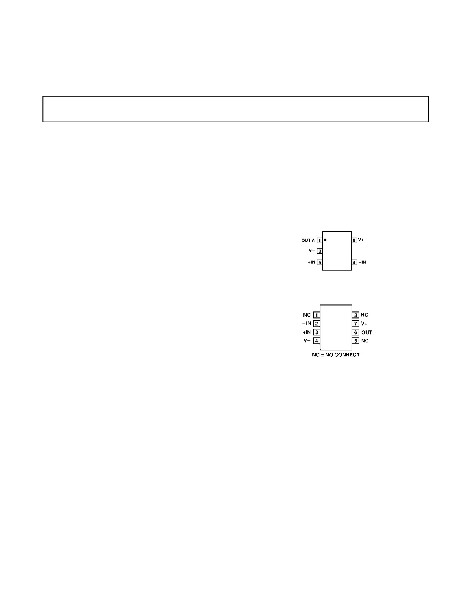
5-Lead SOT
(RT-5)
8-Lead SO
(R-8)
AD8628
AD8628
Specifications

PRELIMINARY TECHNICAL DATA
AD8628
≠ 2 ≠
REV. PrA 1/29/02
ELECTRICAL SPECIFICATIONS
(@ VS=+5.0V, VCM = +2.5V, VO=+2.5V, TA=+25∞C unless otherwise specified.)
Parameter
Symbol
Conditions
Min
Typ
Max
Units
INPUT CHARACTERISTICS
Offset Voltage
V
OS
1 5
µV
-40∞C
T
A
+125∞C
10
µV
Input Bias Current
I
B
30
100
pA
-40∞C
T
A
+125∞C
1.5
nA
Input Offset Current
I
OS
50 200
pA
-40∞C
T
A
+125∞C
250
pA
Input Voltage Range
0
5
V
Common-Mode Rejection Ratio
CMRR
V
CM
= 0V to 5V
120
140
dB
-40∞C
T
A
+125∞C
115
130
dB
Large Signal Voltage Gain (Note 1)
A
VO
R
L
= 10 k
, Vo=0.3 to 4.7V
125
145
dB
-40∞C
T
A
+125∞C
120
135
dB
Offset Voltage Drift
V
OS
/
T -40∞C
T
A
+125∞C
0.002
0.03
µV/∞C
OUTPUT CHARACTERISTICS
Output Voltage High
V
OH
R
L
= 100k
to Ground
4.99
4.996
V
-40∞C
T
A
+125∞C
4.99
4.995
V
R
L
= 10k
to Ground
4.95
4.98
V
-40∞C
T
A
+125∞C
4.95
4.97
V
Output Voltage Low
V
OL
R
L
= 100k
to V+
1
10
mV
-40∞C
T
A
+125∞C
2
10
mV
R
L
= 10 k
to V+
10
20
mV
-40∞C
T
A
+125∞C
15
20
mV
Short Circuit Limit
I
SC
± 25
± 50
mA
-40∞C
T
A
+125∞C
± 40
mA
Output Current
I
O
±
30
mA
-40∞C
T
A
+125∞C
± 15
mA
POWER SUPPLY
Power Supply Rejection Ratio
PSRR
V
S
= 2.7V to 5.5V
120
130
dB
-40∞C
T
A
+125∞C
115
130
dB
Supply Current/Amplifier
I
SY
V
O
= 0V
1.3
1.5
mA
-40∞C
T
A
+125∞C
1.6
1.8
mA
DYNAMIC PERFORMANCE
Slew Rate
SR
R
L
=10 k
0.8
V/µs
Overload Recovery Time
0.05
0.2
ms
Gain Bandwidth Product
GBP
2.5
MHz
NOISE PERFORMANCE
Voltage Noise
e
n p-p
0.1 to 10 Hz
0.5
µV
p-p
Voltage Noise
e
n p-p
0.1 to 1.0 Hz
0.16
µV
p-p
Voltage Noise Density
e
n
f = 1 kHz
22
nV/
Hz
Current Noise Density
in f=10
Hz
5
fA/
Hz
Note 1: Gain testing is highly dependent upon test bandwidth.

PRELIMINARY TECHNICAL DATA
AD8628
≠ 3 ≠
ELECTRICAL SPECIFICATIONS
(@ VS=+2.7V, VCM = +1.35 V, VO=1.4V, TA=+25∞C unless otherwise specified.)
Parameter
Symbol
Conditions
Min
Typ
Max
Units
INPUT CHARACTERISTICS
Offset Voltage
AD8628
V
OS
1 5
µV
-40∞C
T
A
+125∞C
10
µV
Input Bias Current
I
B
30
100
pA
-40∞C
T
A
+125∞C
1.0
1.5
nA
Input Offset Current
I
OS
50 200
pA
-40∞C
T
A
+125∞C
250
pA
Input Voltage Range
0
5
V
Common-Mode Rejection Ratio
CMRR
V
CM
= 0 to 2.9V
115
130
dB
-40∞C
T
A
+125∞C
110
120
dB
Large Signal Voltage Gain
A
VO
R
L
= 10 k
, Vo=0.3 to 4.7V
110
140
dB
-40∞C
T
A
+125∞C
105
130
dB
Offset Voltage Drift
V
OS
/
T -40∞C
T
A
+125∞C
0.002
0.03
µV/∞C
OUTPUT CHARACTERISTICS
Output Voltage High
V
OH
R
L
= 100k
to Ground
2.68
2.695
V
-40∞C
T
A
+125∞C
2.68
2.695
V
R
L
= 10k
to Ground
2.67
2.68
V
-40∞C
T
A
+125∞C
2.67
2.675
V
Output Voltage Low
V
OL
R
L
= 100k
to V+
1
10
mV
-40∞C
T
A
+125∞C
2
10
mV
R
L
= 10 k
to V+
10
20
mV
-40∞C
T
A
+125∞C
15
20
mV
Short Circuit Limit
I
SC
±10
±
15
mA
-40∞C
T
A
+125∞C
± 10
mA
Output Current
I
O
±
10
mA
-40∞C
T
A
+125∞C
± 5
mA
POWER SUPPLY
Power Supply Rejection Ratio
PSRR
V
S
= 2.7V to 5.5 V
120
130
dB
-40∞C
T
A
+125∞C
115
130
dB
Supply Current/Amplifier
I
SY
V
O
= 0V
1.1
1.4
mA
-40∞C
T
A
+125∞C
1.3
1.6
mA
DYNAMIC PERFORMANCE
Slew Rate
SR
R
L
=10 k
1
V/µs
Overload Recovery Time
0.05
ms
Gain Bandwidth Product
GBP
2
MHz
NOISE PERFORMANCE
Voltage Noise
e
n p-p
0.1 to 10 Hz
0.75
µV
p-p
Voltage Noise Density
e
n
f = 1 kHz
33
nV/
Hz
Current Noise Density
in f=10
Hz
5
fA/
Hz
Specifications

PRELIMINARY TECHNICAL DATA
AD8628
≠ 4 ≠
REV. PrA 1/29/02
ABSOLUTE MAXIMUM RATINGS
Supply Voltage ..........................................................................+6V
Input Voltage......................................................GND to Vs + 0.3V
Differential Input Voltage
1
.....................................................
±
5.0V
Output Short-Circuit Duration to Gnd...............................Indefinite
Storage Temperature Range
RT, R Package ...............................................-65∞C to +150∞C
Operating Temperature Range
AD8628 .........................................................-40∞C to +125∞C
Junction Temperature Range
RT, R Package ...............................................-65∞C to +150∞C
Lead Temperature Range (Soldering, 10 sec).......................+300∞C
Package Type
JA
2
JC Units
5-Pin SOT23 (RT)
∞C/W
8-Pin SOIC (R)
158
43
∞C/W
NOTES
1 Differential input voltage is limited to ±5.0 volts or the supply voltage, whichever is less.
2
JA is specified for the worst case conditions, i.e.,
JA is specified for device in socket
for P-DIP packages;
JAis specified for device soldered in circuit board for SOIC and
TSSOP packages.
ORDERING GUIDE
Temperature
Package Package
Model Range
Description Option
AD8628ART -40∞C to +125∞C 5-Pin SOT23
RT-5
AD8628AR
-40∞C to +125∞C 8-Pin SOIC
SO-8