 | –≠–ª–µ–∫—Ç—Ä–æ–Ω–Ω—ã–π –∫–æ–º–ø–æ–Ω–µ–Ω—Ç: AD8631 | –°–∫–∞—á–∞—Ç—å:  PDF PDF  ZIP ZIP |

REV. 0
Information furnished by Analog Devices is believed to be accurate and
reliable. However, no responsibility is assumed by Analog Devices for its
use, nor for any infringements of patents or other rights of third parties
which may result from its use. No license is granted by implication or
otherwise under any patent or patent rights of Analog Devices.
a
AD8631/AD8632
One Technology Way, P.O. Box 9106, Norwood, MA 02062-9106, U.S.A.
Tel: 781/329-4700
World Wide Web Site: http://www.analog.com
Fax: 781/326-8703
© Analog Devices, Inc., 2000
1.8 V, 5 MHz Rail-to-Rail
Low Power Operational Amplifiers
PIN CONFIGURATIONS
5-Lead SOT-23
(RT Suffix)
1
2
3
5
4 ≠IN A
+IN A
V+
OUT A
AD8631
V≠
8-Lead SOIC
(R Suffix)
OUT A
≠IN A
+IN A
V≠
V+
OUT B
≠IN B
+IN B
AD8632
1
8
2
7
3
6
4
5
8-Lead SOIC
(RM Suffix)
≠IN A
+IN A
V≠
OUT B
≠IN B
+IN B
V+
1
4
5
8
AD8632
OUT A
FEATURES
Single Supply Operation: 1.8 V to 6 V
Space-Saving SOT-23, SOIC Packaging
Wide Bandwidth: 5 MHz @ 5 V, 4 MHz @ 1.8 V
Low Offset Voltage: 4 mV Max, 0.8 mV typ
Rail-to-Rail Input and Output Swing
2 V/ s Slew Rate @ 1.8 V
Only 225 A Supply Current @ 1.8 V
APPLICATIONS
Portable Communications
Portable Phones
Sensor Interface
Active Filters
PCMCIA Cards
ASIC Input Drivers
Wearable Computers
Battery-Powered Devices
New Generation Phones
Personal Digital Assistants
GENERAL DESCRIPTION
The AD8631 brings precision and bandwidth to the SOT-23-5
package at single supply voltages as low as 1.8 V and low supply
current. The small package makes it possible to place the AD8631
next to sensors, reducing external noise pickup.
The AD8631 and AD8632 are rail-to-rail input and output bipolar
amplifiers with a gain bandwidth of 4 MHz and typical voltage
offset of 0.8 mV from a 1.8 V supply. The low supply current and
the low supply voltage makes these parts ideal for battery-powered
applications. The 3 V/
µs slew rate makes the AD8631/AD8632 a
good match for driving ASIC inputs, such as voice codecs.
The AD8631/AD8632 is specified over the extended industrial
(≠40 C to +125 C) temperature range. The AD8631 single is
available in 5-lead SOT-23 surface-mount packages. The dual
AD8632 is available in 8-lead SOIC and
µSOIC packages.

≠2≠
REV. 0
AD8631/AD8632≠SPECIFICATIONS
ELECTRICAL CHARACTERISTICS
Parameter
Symbol
Conditions
Min
Typ
Max
Unit
INPUT CHARACTERISTICS
Offset Voltage
V
OS
0.8
4.0
mV
≠40 C
T
A
+125 C
6
mV
Input Bias Current
I
B
250
nA
≠40 C
T
A
+125 C
500
nA
Input Offset Current
I
OS
±150
nA
≠40 C
T
A
+125 C
550
nA
Input Voltage Range
V
CM
0
5
V
Common-Mode Rejection Ratio
CMRR
0 V
V
CM
5 V,
63
70
dB
≠40 C
T
A
+125 C
56
dB
Large Signal Voltage Gain
A
VO
R
L
= 10 k
, 0.5 V < V
OUT
< 4.5 V
25
V/mV
R
L
= 100 k
, 0.5 V < V
OUT
< 4.5 V
100
400
V/mV
R
L
= 100 k
, ≠40 C T
A
+125 C
100
V/mV
Offset Voltage Drift
V
OS
/
T
3.5
µV/ C
Bias Current Drift
I
B
/
T
400
pA/ C
OUTPUT CHARACTERISTICS
Output Voltage Swing High
V
OH
I
L
= 100
µA
≠40 C
T
A
+125 C
4.965
V
I
L
= 1 mA
4.7
V
Output Voltage Swing Low
V
OL
I
L
= 100
µA
≠40 C
T
A
+125 C
35
mV
I
L
= 1 mA
200
mV
Short Circuit Current
I
SC
Short to Ground, Instantaneous
±10
mA
POWER SUPPLY
Power Supply Rejection Ratio
PSRR
V
S
= 2.2 V to 6 V,
75
90
dB
≠40 C
T
A
+125 C
72
dB
Supply Current/Amplifier
I
SY
V
OUT
= 2.5 V
300
450
µA
≠40 C
T
A
+125 C
650
µA
DYNAMIC PERFORMANCE
Slew Rate
SR
1 V < V
OUT
< 4 V, R
L
= 10 k
3
V/
µs
Gain Bandwidth Product
GBP
5
MHz
Settling Time
T
S
0.1%
860
ns
Phase Margin
m
53
Degrees
NOISE PERFORMANCE
Voltage Noise
e
n
p-p
0.1 Hz to 10 Hz
0.8
µV p-p
Voltage Noise Density
e
n
f = 1 kHz
23
nV/
Hz
Current Noise Density
i
n
f = 1 kHz
1.7
pA/
Hz
Specifications subject to change without notice.
(V
S
= 5 V, V≠ = 0 V, V
CM
= 2.5 V, T
A
= 25 C unless otherwise noted)

≠3≠
REV. 0
AD8631/AD8632
ELECTRICAL CHARACTERISTICS
Parameter
Symbol
Conditions
Min
Typ
Max
Unit
INPUT CHARACTERISTICS
Offset Voltage
V
OS
0.8
4.0
mV
≠40 C
T
A
+125 C
6
mV
Input Bias Current
I
B
250
nA
Input Offset Current
I
OS
±150
nA
Input Voltage Range
V
CM
0
2.2
V
Common-Mode Rejection Ratio
CMRR
0 V
V
CM
2.2 V,
54
70
dB
≠40 C
T
A
+125 C
47
dB
Large Signal Voltage Gain
A
VO
R
L
= 10 k
, 0.5 V < V
OUT
< 1.7 V
25
V/mV
R
L
= 100 k
50
200
V/mV
OUTPUT CHARACTERISTICS
Output Voltage Swing High
V
OH
I
L
= 100
µA
2.165
V
I
L
= 750
µA
1.9
V
Output Voltage Swing Low
V
OL
I
L
= 100
µA
35
mV
I
L
= 750
µA
200
mV
POWER SUPPLY
Supply Current/Amplifier
I
SY
V
OUT
= 1.1 V
250
350
µA
≠40 C
T
A
+125 C
500
µA
DYNAMIC PERFORMANCE
Slew Rate
SR
R
L
= 10 k
2.5
V/
µs
Gain Bandwidth Product
GBP
4.3
MHz
Phase Margin
m
50
Degrees
NOISE PERFORMANCE
Voltage Noise Density
e
n
f = 1 kHz
23
nV/
Hz
Current Noise Density
i
n
f = 1 kHz
1.7
pA/
Hz
Specifications subject to change without notice.
(V
S
= 2.2 V, V≠ = 0 V, V
CM
= 1.1 V, T
A
= 25 C unless otherwise noted)

≠4≠
REV. 0
AD8631/AD8632≠SPECIFICATIONS
ELECTRICAL CHARACTERISTICS
Parameter
Symbol
Conditions
Min
Typ
Max
Unit
INPUT CHARACTERISTICS
Offset Voltage
V
OS
0.8
4.0
mV
0 C
T
A
125 C
6
mV
Input Bias Current
I
B
250
nA
Input Offset Current
I
OS
±150
nA
Input Voltage Range
V
CM
0
1.8
V
Common-Mode Rejection Ratio
CMRR
0 V
V
CM
1.8 V,
0 C
T
A
125 C
49
65
dB
Large Signal Voltage Gain
A
VO
R
L
= 10 k
, 0.5 V < V
OUT
< 1.3 V
20
V/mV
R
L
= 100 k
, 0.5 V < V
OUT
< 1.3 V
40
200
V/mV
OUTPUT CHARACTERISTICS
Output Voltage Swing High
V
OH
I
L
= 100
µA
1.765
V
I
L
= 750
µA
1.5
V
Output Voltage Swing Low
V
OL
I
L
= 100
µA
35
mV
I
L
= 750
µA
200
mV
POWER SUPPLY
Power Supply Rejection Ratio
PSRR
V
S
= 1.7 V to 2.2 V,
68
86
dB
0 C
T
A
125 C
65
dB
Supply Current/Amplifier
I
SY
V
OUT
= 0.9 V
225
325
µA
0 C
T
A
125 C
450
µA
DYNAMIC PERFORMANCE
Slew Rate
SR
R
L
= 10 k
2
V/
µs
Gain Bandwidth Product
GBP
4
MHz
Phase Margin
m
49
Degrees
NOISE PERFORMANCE
Voltage Noise Density
e
n
f = 1 kHz
23
nV/
Hz
Current Noise Density
i
n
f = 1 kHz
1.7
pA/
Hz
Specifications subject to change without notice.
(V
S
= 1.8 V, V≠ = 0 V, V
CM
= 0.9 V, T
A
= 25 C unless otherwise noted)
AD8631/AD8632
≠5≠
REV. 0
ABSOLUTE MAXIMUM RATINGS
1
Supply Voltage . . . . . . . . . . . . . . . . . . . . . . . . . . . . . . . . . . 6 V
Input Voltage
2
. . . . . . . . . . . . . . . . . . . . . . . . . . . GND to V
S
Differential Input Voltage . . . . . . . . . . . . . . . . . . . . . .
±0.6 V
Internal Power Dissipation
SOT-23 (RT) . . . . . . . . . . . . See Thermal Resistance Chart
SOIC (R) . . . . . . . . . . . . . . . See Thermal Resistance Chart
µSOIC (RM) . . . . . . . . . . . . See Thermal Resistance Chart
Output Short-Circuit Duration . . . . . . . . . . . . . . . . Indefinite
Storage Temperature Range
R, RM, and RT Packages . . . . . . . . . . . . . ≠65 C to +150 C
Operating Temperature Range
AD8631, AD8632 . . . . . . . . . . . . . . . . . . ≠40 C to +125 C
Junction Temperature Range
R, RM, and RT Packages . . . . . . . . . . . . . ≠65 C to +150 C
Lead Temperature Range (Soldering, 60 sec) . . . . . . . . 300 C
NOTES
1
Stresses above those listed under Absolute Maximum Ratings may cause perma-
nent damage to the device. This is a stress rating only; functional operation of the
device at these or any other conditions above those listed in the operational sections
of this specification is not implied. Exposure to absolute maximum rating condi-
tions for extended periods may affect device reliability.
2
For supply voltages less than 6 V the input voltage is limited to the supply voltage.
Package Type
JA
1
JC
Unit
5-Lead SOT-23 (RT)
230
146
C/W
8-Lead SOIC (R)
158
43
C/W
8-Lead
µSOIC (RM)
210
45
C/W
NOTE
1
JA
is specified for worst-case conditions, i.e.,
JA
is specified for device soldered
in circuit board for SOT-23 and SOIC packages.
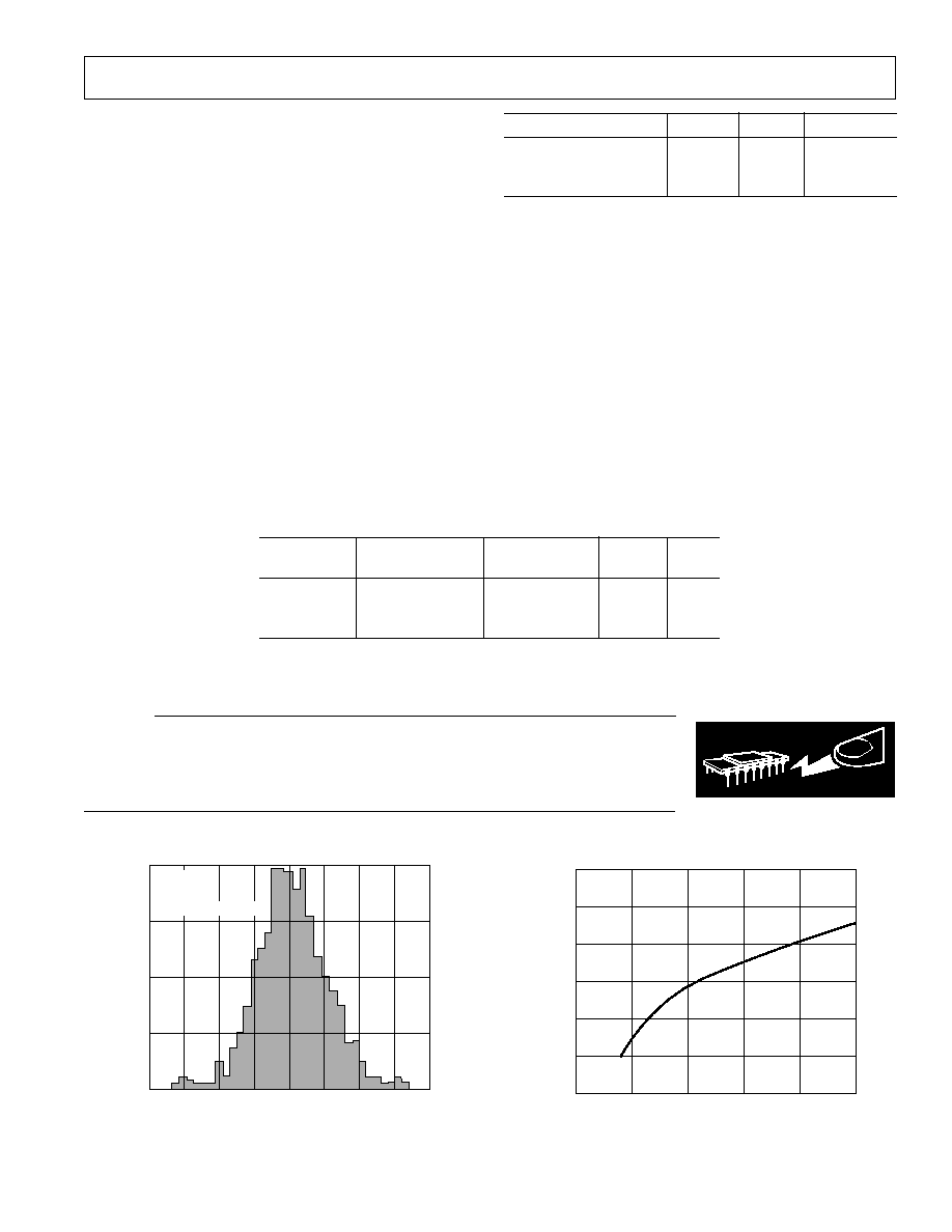
INPUT OFFSET VOLTAGE ≠ mV
120
0
≠4
QUANTITY OF AMPLIFIERS
90
60
30
≠3
≠2
≠1
0
1
2
3
4
V
S
= 5V
V
CM
= 2.5V
T
A
= 25 C
COUNT = 1,133 OP AMPS
Figure 1. Input Offset Voltage Distribution
SUPPLY VOLTAGE ≠ V
350
200
6
SUPPLY CURRENT
≠
A
1
3
4
5
325
300
275
250
225
2
T
A
= 25 C
Figure 2. Supply Current per Amplifier vs. Supply Voltage
CAUTION
ESD (electrostatic discharge) sensitive device. Electrostatic charges as high as 4000 V readily
accumulate on the human body and test equipment and can discharge without detection.
Although the AD8631/AD8632 features proprietary ESD protection circuitry, permanent dam-
age may occur on devices subjected to high energy electrostatic discharges. Therefore, proper
ESD precautions are recommended to avoid performance degradation or loss of functionality.
WARNING!
ESD SENSITIVE DEVICE
ORDERING GUIDE
Temperature
Package
Package
Model
Range
Description
Option
Brand
AD8631ART
1
≠40 C to +125 C
5-Lead SOT-23
RT-5
AEA
AD8632AR
≠40 C to +125 C
8-Lead SOIC
SO-8
AD8632ARM
2
≠40 C to +125 C
8-Lead
µSOIC
RM-8
AGA
NOTES
1
Available in 3,000-piece reels only.
2
Available in 2,500-piece reels only.
AD8631/AD8632
≠6≠
REV. 0
≠ Typical Characteristics
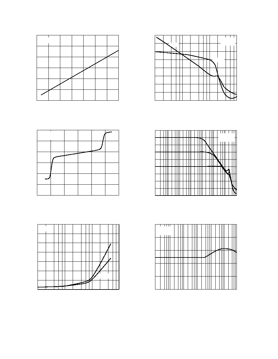
TEMPERATURE ≠ C
500
200
125
SUPPLY CURRENT
≠
A
50
25
50
100
450
400
350
300
250
V
S
= 5V
25
0
75
Figure 3. Supply Current per Amplifier vs. Temperature
COMMON-MODE VOLTAGE ≠ V
150
150
100
50
0
50
100
3
3
2
INPUT BIAS CURRENT
≠
nA
1
0
1
2
V
S
= 2.5V
T
A
= 25 C
Figure 4. Input Bias Current vs. Common-Mode Voltage
SOURCE
LOAD CURRENT ≠ A
140
120
0
10
10k
100
OUTPUT VOLTAGE
≠
mV
1k
100
80
60
40
20
T
A
= 25 C
Figure 5. Output Voltage to Supply Rail vs. Load Current
FREQUENCY ≠ Hz
100k
100M
1M
OPEN-LOOP GAIN
≠
dB
10M
40
40
30
20
10
0
10
20
30
45
0
45
90
90
PHASE SHIFT
≠
De
g
rees
V
S
= 5V
T
A
= 25 C
GAIN
PHASE
Figure 6. Open-Loop Gain vs. Frequency
FREQUENCY ≠ Hz
10
100M
1k
CLOSED-LOOP GAIN
≠
dB
1M
40
40
20
20
50
100
10k
100k
10M
V
S
= ±2.5V
T
A
= 25 C
30
10
0
10
30
Figure 7. Closed-Loop Gain vs. Frequency
FREQUENCY ≠ Hz
10
1k
CMRR
≠
dB
1M
100
20
40
60
80
0
100
10k
100k
10M
V
S
= 2.5V
T
A
= 25 C
Figure 8. CMRR vs. Frequency

AD8631/AD8632
≠7≠
REV. 0
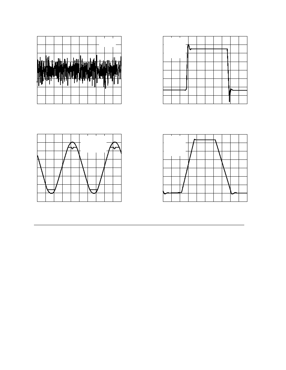
FREQUENCY ≠ Hz
10
1k
PSRR
≠
dB
1M
20
40
60
80
0
100
10k
100k
10M
120
PSRR
V
S
= 2.5V
T
A
= 25 C
PSRR
100
Figure 9. PSRR vs. Frequency
V
S
= 5V
V
CM
= 2.5V
R
L
= 10k
T
A
= 25 C
V
IN
= 50mV
A
V
= +1
CAPACITANCE ≠ pF
60
50
0
10
100
OVERSHOOT
≠
%
30
20
10
40
OS
+OS
Figure 10. Overshoot vs. Capacitance Load
FREQUENCY ≠ Hz
6
5
0
10k
1M
100k
MAXIMUM OUTPUT SWING
≠
V p-p
3
2
1
4
DISTORTION 3%
V
S
= 5V
A
V
= +1
R
L
= 10k
T
A
= 25 C
C
L
= 15pF
Figure 11. Output Swing vs. Frequency
FREQUENCY ≠ Hz
10
100M
1k
OUTPUT IMPEDANCE
≠
1M
0
60
40
100
10k
100k
10M
V
S
= 5V
T
A
= 25 C
10
20
30
50
A
V
= +10
A
V
= +1
Figure 12. Output Impedance vs. Frequency
FREQUENCY ≠ Hz
50
0
10
10k
100
VOLTAGE NOISE DENSITY
≠
pA/
Hz
1k
40
30
20
10
V
S
=5V
T
A
= 25 C
Figure 13. Voltage Noise Density vs. Frequency
FREQUENCY ≠ Hz
5
0
10
10k
100
CURRENT NOISE DENSITY
≠
pA/
Hz
1k
4
3
2
1
V
S
= 5V
T
A
= 25 C
Figure 14. Current Noise Density vs. Frequency
AD8631/AD8632
≠8≠
REV. 0
VOLTAGE
≠
200nV/DIV
TIME ≠ 1s/DIV
0
0
0
0
0
0
0
0
0
T
A
= 25 C
V
S
= 2.5V
Figure 15. 0.1 Hz to 10 Hz Noise
TIME ≠ 200 s/DIV
0
0
0
VOLTAGE
≠
1V/DIV
0
0
0
0
0
V
S
= 2.5V
A
V
= 1
V
IN
= SINE WAVE
T
A
= 25 C
Figure 16. No Phase Reversal
TIME ≠ 250ns/DIV
0
0
0
VOLTAGE
≠
20mV/DIV
0
0
0
0
0
V
S
= 2.5V
A
V
= +1
T
A
= 25 C
C
L
= 33pF
R
L
= 10k
Figure 17. Small Signal Transient Response
TIME ≠ 500ns/DIV
0
0
0
VOLTAGE
≠
500mV/DIV
0
0
0
0
0
V
S
= 2.5V
A
V
= +1
T
A
= 25 C
C
L
= 100pF
R
L
= 10k
Figure 18. Large Signal Transient Response
THEORY OF OPERATION
The AD863x is a rail-to-rail operational amplifier that can operate
at supply voltages as low as 1.8 V. This family is fabricated using
Analog Devices' high-speed complementary bipolar process, also
called XFCB. The process trench isolates each transistor to mini-
mize parasitic capacitance, thereby allowing high-speed perfor-
mance. Figure 19 shows a simplified schematic of the AD863x
family.
The input stage consists of two parallel complementary differen-
tial pair: one NPN pair (Q1 and Q2) and one PNP pair (Q3 and
Q4). The voltage drops across R7, R8, R9, and R10 are kept low
for rail-to-rail operation. The major gain stage of the op amp is a
double-folded cascode consisting of transistors Q5, Q6, Q8, and
Q9. The output stage, which also operates rail-to-rail, is driven by
Q14. The transistors Q13 and Q10 act as level-shifters to give
more headroom during 1.8 V operation.
As the voltage at the base of Q13 increases, Q18 starts to sink
current. When the voltage at the base of Q13 decreases I8 flows
through D16 and Q15 increasing the VBE of Q17, then Q20
sources current.
The output stage also furnishes gain, which depends on the load
resistance, since the output transistors are in common emitter
configuration. The output swing when sinking or sourcing 100
µA
is 35 mV maximum from each rail.
The input bias current characteristics depend on the common-
mode voltage (see Figure 4). As the input voltage reaches about
1 V below V
CC
, the PNP pair (Q3 and Q4) turns off.
The 1 k
input resistor R1 and R2, together with the diodes D7
and D8, protect the input pairs against avalanche damage.
The AD863x family exhibits no phase reversal as the input signal
exceeds the supply by more than 0.6 V. Excessive current can flow
through the input pins via the ESD diodes D1-D2 or D3-D4, in the
event their ~0.6 V thresholds are exceeded. Such fault currents must
be limited to 5 mA or less by the use of external series resistance(s).
LOW VOLTAGE OPERATION
Battery Voltage Discharge
The AD8631 operates at supply voltages as low as 1.8 V. This
amplifier is ideal for battery-powered applications since it can
operate at the end of discharge voltage of most popular batteries.
Table I lists the Nominal and End-of-Discharge Voltages of
several typical batteries.

AD8631/AD8632
≠9≠
REV. 0
The rail-to-rail feature of the AD8631 can be observed over the
supply voltage range, 1.8 V to 5 V. Traces are shown offset for
clarity.
INPUT BIAS CONSIDERATION
The input bias current (I
B
) is a non-ideal, real-life parameter that
affects all op amps. I
B
can generate a somewhat significant offset
voltage. This offset voltage is created by I
B
when flowing through
the negative feedback resistor R
F
. If I
B
is 250 nA (worst case), and
R
F
is 100 k
, the corresponding generated offset voltage is 25 mV
(V
OS
= I
B
R
F
).
Obviously the lower the R
F
the lower the generated voltage offset.
Using a compensation resistor, R
B
, as shown in Figure 21, can
minimize this effect. With the input bias current minimized we
still need to be aware of the input offset current (I
OS
) which will
generate a slight offset error. Figure 21 shows three different
configurations to minimize I
B
-induced offset errors.
NONINVERTING CONFIGURATION
AD8631
R
S
V
I
V
OUT
R
F
= R
S
UNITY GAIN BUFFER
V
OUT
R
F
R
I
R
B
= R
I
R
F
V
I
V
OUT
R
B
= R
I
R
F
V
I
R
F
R
I
AD8631
INVERTING CONFIGURATION
AD8631
Figure 21. Input Bias Cancellation Circuits
Q14
IN
V
EE
V
CC
V
OUT
Q1
Q3
R5
R6
I2
R1
IN
R2
R4
R3
I1
R7
R8
D2
ESD
D7
D8
Q2
Q4
D1
ESD
D3
ESD
D4
ESD
Q5
Q6
Q7
C1
Q8
Q11
Q9
I4
I3
I5
Q13
I7
I6
C3
R10
R9
R11
Q15
Q17
D6
R12
Q18
I8
C2
R14
Q19
Q20
C4
D9
V
CC
D16
R13
V
EE
Q10
Figure 19. Simplified Schematic
Table I. Typical Battery Life Voltage Range
Nominal
End-of-Voltage
Battery
Voltage (V)
Discharge (V)
Lead-Acid
2
1.8
Lithium
2.6≠3.6
1.7≠2.4
NiMH
1.2
1
NiCd
1.2
1
Carbon-Zinc
1.5
1.1
RAIL-TO-RAIL INPUT AND OUTPUT
The AD8631 features an extraordinary rail-to-rail input and
output with supply voltages as low as 1.8 V. With the amplifier's
supply set to 1.8 V, the input can be set to 1.8 V p-p, allowing the
output to swing to both rails without clipping. Figure 20 shows a
scope picture of both input and output taken at unity gain, with a
frequency of 1 kHz, at V
S
= 1.8 V and V
IN
= 1.8 V p-p.
TIME ≠ 200 s/Div
V
S
= 1.8V
V
IN
= 1.8V p-p
V
IN
V
OUT
Figure 20. Rail-to-Rail Input Output

AD8631/AD8632
≠10≠
REV. 0
DRIVING CAPACITIVE LOADS
Capacitive Load vs. Gain
Most amplifiers have difficulty driving capacitance due to degra-
dation of phase margin caused by additional phase lag from the
capacitive load. Higher capacitance at the output can increase the
amount of overshoot and ringing in the amplifier's step response
and could even affect the stability of the device. The value of
capacitive load that an amplifier can drive before oscillation varies
with gain, supply voltage, input signal, temperature, among oth-
ers. Unity gain is the most challenging configuration for driving
capacitive load. However, the AD8631 offers reasonably good
capacitive driving ability. Figure 22 shows the AD8631's ability to
drive capacitive loads at different gains before instability occurs.
This graph is good for all V
SY
.
GAIN ≠ V/V
1M
10
10
2
CAPACITIVE LOAD
≠
pF
4
6
8
10k
1k
100
9
3
5
7
1
UNSTABLE
STABLE
100k
Figure 22. Capacitive Load vs. Gain
In-the-Loop Compensation Technique for Driving
Capacitive Loads
When driving capacitance in low gain configuration, the in-the-loop
compensation technique is recommended to avoid oscillation as is
illustrated in Figure 23.
R
F
+
R
G
C
F
=
1
+
A
CL
1
R
F
C
L
R
O
[
[
R
X
=
R
O
R
G
R
F
WHERE R
O
= OPEN-LOOP OUTPUT RESISTANCE
AD8631
V
IN
V
OUT
R
X
C
L
C
F
R
F
R
G
Figure 23. In-the-Loop Compensation Technique for
Driving Capacitive Loads
Snubber Network Compensation for Driving Capacitive Loads
As load capacitance increases, the overshoot and settling time
will increase and the unity gain bandwidth of the device will
decrease. Figure 24 shows an example of the AD8631 in a non-
inverting configuration driving a 10 k
resistor and a 600 pF
capacitor placed in parallel, with a square wave input set to a
frequency of 90 kHz and unity gain.
VOLTAGE
≠
200mV/DIV
TIME ≠ 2 s/DIV
90kHz INPUT SIGNAL
A
V
= 1
C = 600pF
Figure 24. Driving Capacitive Loads without Compensation
By connecting a series R≠C from the output of the device to
ground, known as the "snubber" network, this ringing and over-
shoot can be significantly reduced. Figure 25 shows the network
setup, and Figure 26 shows the improvement of the output
response with the "snubber" network added.
AD8631
V
IN
V
OUT
5V
R
X
C
X
C
L
Figure 25. Snubber Network Compensation for Capacitive
Loads
VOLTAGE
≠
200mV/DIV
TIME ≠ 2 s/DIV
90kHz INPUT SIGNAL
A
V
= 1
C = 600pF
Figure 26. Photo of a Square Wave with the Snubber
Network Compensation
The network operates in parallel with the load capacitor, C
L
,
and provides compensation for the added phase lag. The actual
values of the network resistor and capacitor have to be empirically
determined. Table II shows some values of snubber network for
large capacitance load.

AD8631/AD8632
≠11≠
REV. 0
Table II. Snubber Network Values for Large Capacitive Loads
C
LOAD
Rx
Cx
600 pF
300
1 nF
1 nF
300
1 nF
10 nF
90
8
nF
TOTAL HARMONIC DISTORTION + NOISE
The AD863x family offers a low total harmonic distortion, which
makes this amplifier ideal for audio applications. Figure 27 shows
a graph of THD + N, which is ~0.02% @ 1 kHz, for a 1.8 V supply.
At unity gain in an inverting configuration the value of the Total
Harmonic Distortion + Noise stays consistently low over all volt-
ages supply ranges.
FREQUENCY ≠ Hz
0.1
0.001
10
20k
THD + N
≠
%
0.01
1
10
100
1k
10k
V
S
= 1.8V
V
S
= 5V
INVERTING
A
V
= 1
Figure 27. THD + N vs. Frequency Graph
AD8632 Turn-On Time
The low voltage, low power AD8632 features an extraordinary turn
on time. This is about 500 ns for V
SY
= 5 V, which is impressive
considering the low supply current (300
µA typical per amplifier).
Figure 28 shows a scope picture of the AD8632 with both channels
configured as followers. Channel A has an input signal of 2.5 V and
channel B has the input signal at ground. The top waveform shows
the supply voltage and the bottom waveform reflects the response
of the amplifier at the output of Channel A.
TIME ≠ 200ns/DIV
0
0
0
VOLTAGE
≠
1V/DIV
0
0
0
0
V
S
= 5V
A
V
= 1
V
IN
= 2.5V STEP
0V
0V
Figure 28. AD8632 Turn-On Time
A MICROPOWER REFERENCE VOLTAGE GENERATOR
Many single-supply circuits are configured with the circuit biased
to one-half of the supply voltage. In these cases, a false-ground
reference can be created by using a voltage divider buffered by an
amplifier. Figure 28 shows the schematic for such a circuit.
The two 1 M
resistors generate the reference voltages while
drawing only 0.9
µA of current from a 1.8 V supply. A capacitor
connected from the inverting terminal to the output of the op
amp provides compensation to allow a bypass capacitor to be
connected at the reference output. This bypass capacitor helps
establish an ac ground for the reference output.
AD8631
10k
0.022 F
V
REF
0.9V TO 2.5V
1 F
1 F
1M
1.8V TO 5V
100
1M
Figure 29. A Micropower Reference Voltage Generator
MICROPHONE PREAMPLIFIER
The AD8631 is ideal to use as a microphone preamplifier.
Figure 30 shows this implementation.
AD8631
V
OUT
R3
220k
1.8V
V
REF
= 0.9V
R2
22k
C1
0.1 F
1.8V
R1
2.2k
ELECTRET
MIC
A
V
= R3
R2
V
IN
Figure 30. A Microphone Preamplifier
R1 is used to bias an electret microphone and C1 blocks dc voltage
from the amplifier. The magnitude of the gain of the amplifier is
approximately R3/R2 when R2
10 R1. V
REF
should be equal to
1/2
1.8 V for maximum voltage swing.
Direct Access Arrangement for Telephone Line Interface
Figure 31 illustrates a 1.8 V transmit/receive telephone line interface
for 600
transmission systems. It allows full duplex transmission of
signals on a transformer-coupled 600
line in a differential manner.
Amplifier A1 provides gain that can be adjusted to meet the modem
output drive requirements. Both A1 and A2 are configured to apply
the largest possible signal on a single supply to the transformer.
Amplifier A3 is configured as a difference amplifier for two reasons:
(1) It prevents the transmit signal from interfering with the receive
signal and (2) it extracts the receive signal from the transmission line
for amplification by A4. A4's gain can be adjusted in the same
manner as A1's to meet the modem's input signal requirements.
Standard resistor values permit the use of SIP (Single In-line
Package) format resistor arrays. Couple this with the AD8631/

≠12≠
REV. 0
PRINTED IN U.S.A.
AD8631/AD8632
C3810≠2.5≠4/00 (rev. 0)
AD8632's 5-lead SOT-23, 8-lead
µSOIC, and 8-lead SOIC
footprint and this circuit offers a compact solution.
6.2V
6.2V
TRANSMIT
TxA
RECEIVE
RxA
C1
0.1 F
R1
10k
R2
9.09k
2k
P1
Tx GAIN
ADJUST
A1
A2
A3
A4
A1, A2 = 1/2 AD8632
A3, A4 = 1/2 AD8632
R3
360
1:1
T1
TO TELEPHONE
LINE
1
2
3
7
6
5
2
3
1
6
5
7
10 F
R7
10k
R8
10k
R5
10k
R6
10k
R9
10k
R14
14.3k
R10
10k
R11
10k
R12
10k
R13
10k
C2
0.1 F
P2
Rx GAIN
ADJUST
2k
Z
O
600
+1.8V DC
MIDCOM
671-8005
Figure 31. A Single-Supply Direct Access Arrangement
for Modems
OUTLINE DIMENSIONS
Dimensions shown in inches and (mm).
8-Lead Narrow Body SOIC
(SO-8)
0.1968 (5.00)
0.1890 (4.80)
8
5
4
1
0.2440 (6.20)
0.2284 (5.80)
PIN 1
0.1574 (4.00)
0.1497 (3.80)
0.0688 (1.75)
0.0532 (1.35)
SEATING
PLANE
0.0098 (0.25)
0.0040 (0.10)
0.0192 (0.49)
0.0138 (0.35)
0.0500
(1.27)
BSC
0.0098 (0.25)
0.0075 (0.19)
0.0500 (1.27)
0.0160 (0.41)
8
0
0.0196 (0.50)
0.0099 (0.25)
45
5-Lead SOT-23
(RT-5)
0.1181 (3.00)
0.1102 (2.80)
PIN 1
0.0669 (1.70)
0.0590 (1.50)
0.1181 (3.00)
0.1024 (2.60)
1
3
4
5
0.0748 (1.90)
BSC
0.0374 (0.95) BSC
2
0.0079 (0.20)
0.0031 (0.08)
0.0217 (0.55)
0.0138 (0.35)
10
0
0.0197 (0.50)
0.0138 (0.35)
0.0059 (0.15)
0.0019 (0.05)
0.0512 (1.30)
0.0354 (0.90)
SEATING
PLANE
0.0571 (1.45)
0.0374 (0.95)
8-Lead SOIC
(RM-8)
8
5
4
1
0.122 (3.10)
0.114 (2.90)
0.199 (5.05)
0.187 (4.75)
PIN 1
0.0256 (0.65) BSC
0.122 (3.10)
0.114 (2.90)
SEATING
PLANE
0.006 (0.15)
0.002 (0.05)
0.018 (0.46)
0.008 (0.20)
0.043 (1.09)
0.037 (0.94)
0.120 (3.05)
0.112 (2.84)
0.011 (0.28)
0.003 (0.08)
0.028 (0.71)
0.016 (0.41)
33
27
0.120 (3.05)
0.112 (2.84)
SPICE Model
The SPICE model for the AD8631 amplifier is available and
can be downloaded from the Analog Devices' web site at
http://www.analog.com. The macro-model accurately simulates
a number of AD8631 parameters, including offset voltage, input
common-mode range, and rail-to-rail output swing. The output
voltage versus output current characteristics of the macro-model
is identical to the actual AD8631 performance, which is a critical
feature with a rail-to-rail amplifier model. The model also accurately
simulates many ac effects, such as gain-bandwidth product, phase
margin, input voltage noise, CMRR and PSRR versus frequency,
and transient response. Its high degree of model accuracy makes the
AD8631 macro-model one of the most reliable and true-to-life
models available for any amplifier.