 | ÐлекÑÑоннÑй компоненÑ: AD8698 | СкаÑаÑÑ:  PDF PDF  ZIP ZIP |
Äîêóìåíòàöèÿ è îïèñàíèÿ www.docs.chipfind.ru
Dual Precision, Rail-to-Rail Output
Operational Amplifier
AD8698
Rev. 0
Information furnished by Analog Devices is believed to be accurate and reliable.
However, no responsibility is assumed by Analog Devices for its use, nor for any
infringements of patents or other rights of third parties that may result from its use.
Specifications subject to change without notice. No license is granted by implication
or otherwise under any patent or patent rights of Analog Devices. Trademarks and
registered trademarks are the property of their respective owners.
One Technology Way, P.O. Box 9106, Norwood, MA 02062-9106, U.S.A.
Tel: 781.329.4700
www.analog.com
Fax: 781.326.8703
© 2004 Analog Devices, Inc. All rights reserved.
FEATURES
Low offset voltage: 100 µV max
Low offset voltage drift: 2
µV/°C max
Low input bias current: 700 pA max
Low noise: 8 nV/
Hz
High common-mode rejection: 118 dB min
Wide operating temperature:
-40°C to +85°C
No phase reversal
APPLICATIONS
Photodiode amplifier
Sensors and controls
Multipole filters
Integrator
GENERAL DESCRIPTION
The AD8698 is a high precision, rail-to-rail output, low noise,
low input bias current operational amplifier. Offset voltage is a
respectable 100 µV max and drift over temperature is below
2 µV/°C, eliminating the need for manual offset trimming. The
AD8698 is ideal for high impedance sensors, minimizing offset
errors due to input bias and offset currents.
The rail-to-rail output maximizes dynamic range in a variety of
applications, such as photodiode amplifiers, DAC I/V
amplifiers, filters, and ADC input amplifiers.
The AD8698 dual amplifiers are offered in 8-lead MSOP and
narrow 8-lead SOIC packages. The MSOP version is available
in tape and reel only.
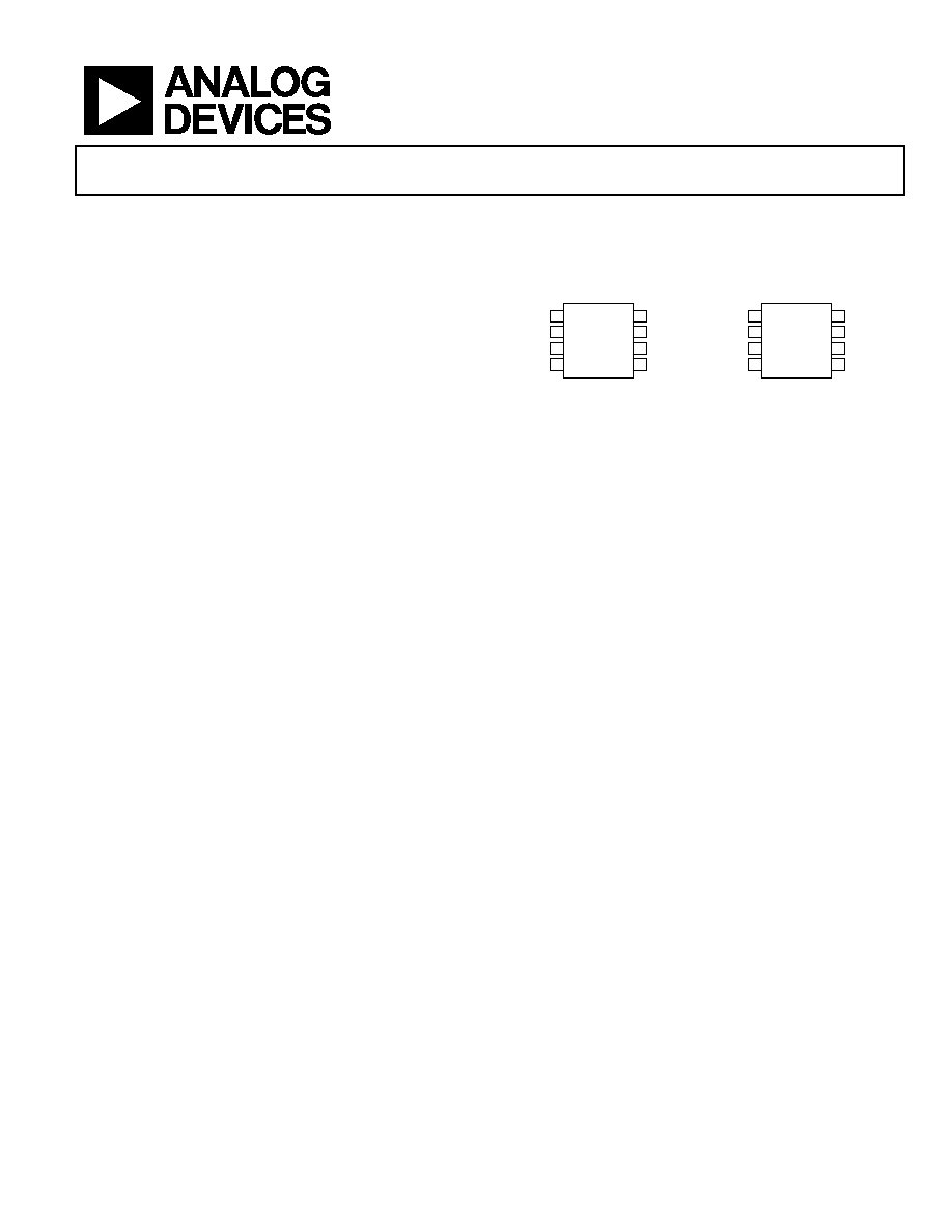
CONNECTION DIAGRAMS
8-Lead SOIC
(R-8)
OUT A
1
IN A
2
+IN A
3
V
4
V+
8
OUT B
7
IN B
6
+IN B
5
AD8698
TOP VIEW
(Not to Scale)
04807-0-069
8-Lead MSOP
(RM-8)
OUT A
1
IN A
2
+IN A
3
V
4
V+
8
OUT B
7
IN B
6
+IN B
5
AD8698
TOP VIEW
(Not to Scale)
04807-0-070
Figure 1.

AD8698
Rev. 0 | Page 2 of 20
TABLE OF CONTENTS
Specifications .................................................................................... 3
Absolute Maximum Ratings ........................................................... 5
Thermal Resistance ...................................................................... 5
ESD Caution.................................................................................. 5
Typical Performance Characteristics............................................. 6
Applications .................................................................................... 14
Input Overvoltage Protection................................................... 14
Driving Capacitive Loads .......................................................... 14
Instrumentation Amplifier ....................................................... 15
Composite Amplifier ................................................................. 15
Low Noise Applications ............................................................ 16
Driving ADCs ............................................................................. 16
Using the AD8698 in Active Filter Designs ........................... 16
Outline Dimensions....................................................................... 17
Ordering Guide .......................................................................... 17
REVISION HISTORY
4/04--Revision 0: Initial Version

AD8698
Rev. 0 | Page 3 of 20
SPECIFICATIONS
V
S
= ±15 V, V
CM
= 0 V (@T
A
= 25
o
C, unless otherwise noted.)
Table 1.
Parameter Symbol
Conditions
Min
Typ
Max
Unit
INPUT CHARACTERISTICS
Offset Voltage
V
OS
20
100
µV
-40°C < T
A
< +85°C
300
µV
Offset Voltage Drift
V
OS
/
T
-40°C < T
A
< +85°C
0.6
2 µV/°C
Input Bias Current
I
B
700
pA
-40°C < T
A
< +85°C
1500
pA
Input Offset Current
I
OS
700
pA
-40°C < T
A
< +85°C
1500
pA
Input Voltage Range
IVR
-40°C < T
A
< +85°C
-13.5V
13.5
V
Common-Mode Rejection Ratio
CMRR
V
CM
= ±13.5 V
118
132
dB
Large Signal Voltage Gain
A
VO
R
L
= 2 k
, V
O
= ±13.5 V
900 1450
V/mV
Input Capacitance
C
DIFF
6.5
pF
C
CM
4.6
pF
OUTPUT CHARACTERISTICS
Output Voltage Swing (Ref. to GND)
V
OH
I
L
= 1 mA,
-40°C < T
A
< +85°C
14.85 14.93
V
V
OH
I
L
= 5 mA,
-40°C < T
A
< +85°C
14.6 14.8
V
(Ref. to GND)
V
OL
I
L
= 1 mA,
-40°C < T
A
< +85°C
-14.93
-14.6
V
V
OL
I
L
= 5 mA,
-40°C < T
A
< +85°C
-14.82
-14.5
V
POWER SUPPLY
Power Supply Rejection Ratio
PSRR
±2.5 V < V
S
< ±15 V
114
132
dB
Supply Current
I
SY
V
O
= 0 V
2.8
3.2
mA
-40°C < T
A
< +85°C
3.8
mA
Supply Voltage
V
S
-40°C < T
A
< +85°C
±2.5
±15 V
DYNAMIC PERFORMANCE
Slew Rate
SR
R
L
= 2 k
0.4
V/µs
Gain Bandwidth Product
GBP
1
MHz
Phase Margin
Ø
O
60 Degrees
NOISE PERFORMANCE
Input Noise Voltage
e
n
p-p
0.1 Hz < f < 10 Hz
0.6
µV p-p
Input Voltage Noise Density
e
n
f = 10 Hz
15
nV/
Hz
Input Voltage Noise Density
e
n
f = 1 kHz
8
nV/
Hz
Current Noise Density
i
n
f = 1 kHz
0.2
pA/
Hz

AD8698
Rev. 0 | Page 4 of 20
V
S
= ±2.5 V, V
CM
= 0 V (@T
A
= 25
o
C, unless otherwise noted.)
Table 2.
Parameter Symbol
Conditions
Min
Typ
Max
Unit
INPUT CHARACTERISTICS
Offset Voltage
V
OS
20
100
µV
-40°C < T
A
< +85°C
300
µV
Offset Voltage Drift
V
OS
/
T
-40°C < T
A
< +85°C
2 µV/°C
Input Bias Current
I
B
700
pA
-40°C < T
A
< +85°C
1500
pA
Input Offset Current
I
OS
700
pA
-40°C < T
A
< +85°C
1500
pA
Input Voltage Range
IVR
-40°C < T
A
< +85°C
-1.5
+1.5
V
Common-Mode Rejection Ratio
CMRR
V
CM
= ±13.5 V
105
120
dB
Large Signal Voltage Gain
A
VO
R
L
= 2 k
, V
O
= ±13.5 V
600 1200
V/mV
Input Capacitance
C
DIFF
6.4
pF
C
CM
4.6
pF
OUTPUT CHARACTERISTICS
Output Voltage Swing (Ref. to GND)
V
OH
I
L
= 1 mA,
-40°C < T
A
< +85°C
2.35 2.44
V
V
OH
I
L
= 5 mA,
-40°C < T
A
< +85°C
2.1 2.29
V
(Ref. to GND)
V
OL
I
L
= 1 mA,
-40°C < T
A
< +85°C
-2.43
-2.2
V
V
OL
I
L
= 5 mA, T
A
= 25°C
-2.15
-1.9
V
I
L
= 5mA,
-40°C<T
A
<+85°C
-1.6
POWER SUPPLY
Power Supply Rejection Ratio
PSRR
±2.5 V < V
S
< ±15 V
114
132
dB
Supply Current
I
SY
V
O
= 0 V
2.3
2.8
mA
-40°C < T
A
< +85°C
3.3
mA
Supply Voltage
Vs
-40°C < T
A
< +85°C
±2.5
±15
V
DYNAMIC PERFORMANCE
Slew Rate
SR
R
L
= 2 k
0.4
V/µs
Gain Bandwidth Product
GBP
1
MHz
Phase Margin
Øo
60
Degrees
NOISE PERFORMANCE
Input Noise Voltage
e
n
p-p
0.1 Hz < f < 10Hz
0.6
µV p-p
Input Voltage Noise Density
e
n
f = 10 Hz
15
nV/
Hz
Input Voltage Noise Density
e
n
f =1 kHz
8
nV/
Hz
Current Noise Density
i
n
f = 1 kHz
0.2
pA/
Hz
AD8698
Rev. 0 | Page 5 of 20
ABSOLUTE MAXIMUM RATINGS
Table 3.
Parameter Rating
Supply Voltage
±15 V
Input Voltage
±V
S
Differential Input Voltage
±V
S
Output Short-Circuit Duration
to Gnd
Indefinite
Storage Temperature Range
R, RM Packages
-65°C to +150°C
Operating Temperature Range
-40°C to +85°C
Junction Temperature Range
R, RM Packages
-65°C to +150°C
Lead Temperature Range
(Soldering, 60 Sec)
+300°C
Stresses above those listed under Absolute Maximum Ratings
may cause permanent damage to the device. This is a stress
rating only; functional operation of the device at these or any
other conditions above those indicated in the operational
section of this specification is not implied. Exposure to absolute
maximum rating conditions for extended periods may affect
device reliability.
THERMAL RESISTANCE
JA
is specified for the worst-case conditions, i.e.,
JA
is specified
for devices soldered in circuit boards for surface-mount
packages.
Table 4. Thermal Resistance
Package Type
JA
JC
Unit
MSOP-8 (RM)
210
45
°C/W
SOIC-8 (R)
158
43
°C/W
ESD CAUTION
ESD (electrostatic discharge) sensitive device. Electrostatic charges as high as 1000 V readily accumulate on the
human body and test equipment and can discharge without detection. Although this product features
proprietary ESD protection circuitry, permanent damage may occur on devices subjected to high energy
electrostatic discharges. Therefore, proper ESD precautions are recommended to avoid performance
degradation or loss of functionality.
AD8698
Rev. 0 | Page 6 of 20
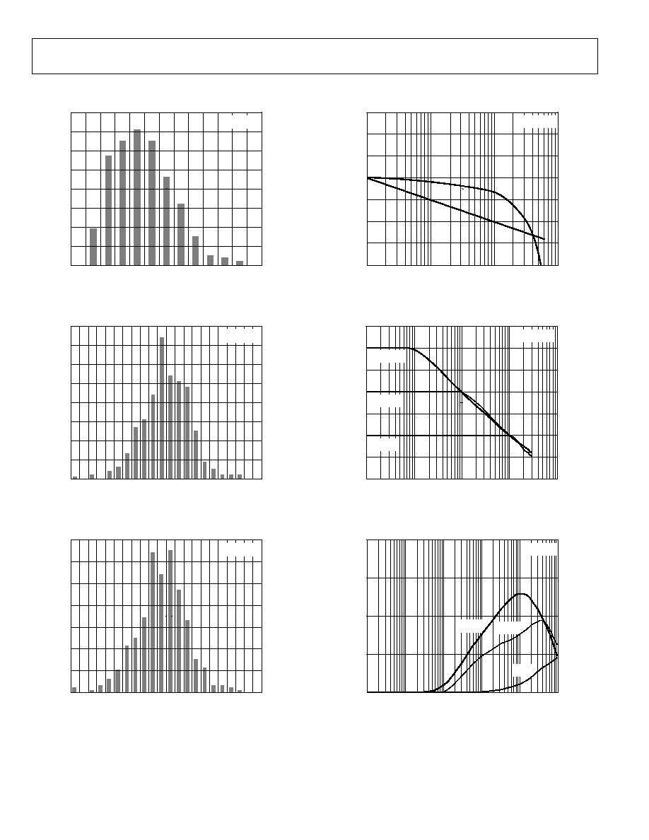
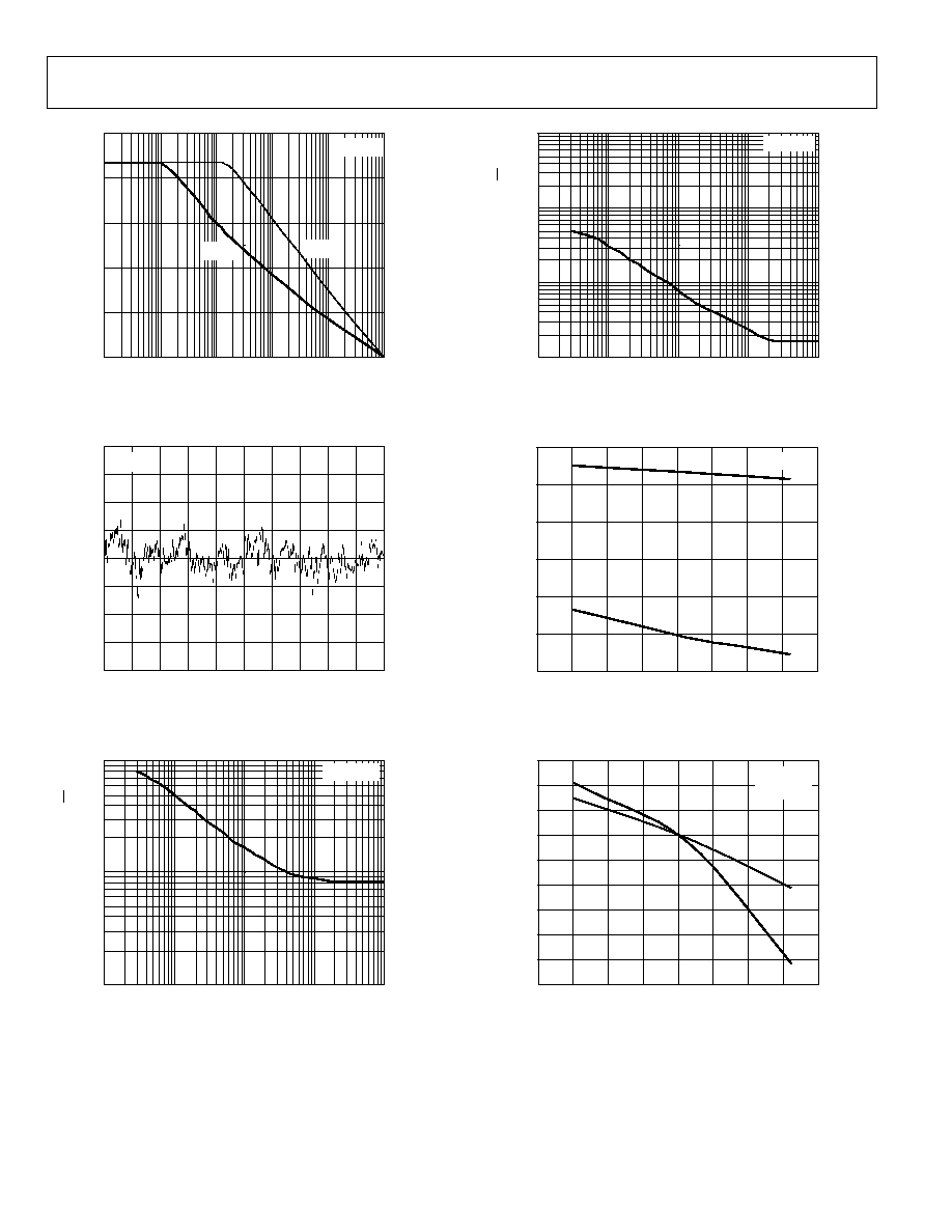
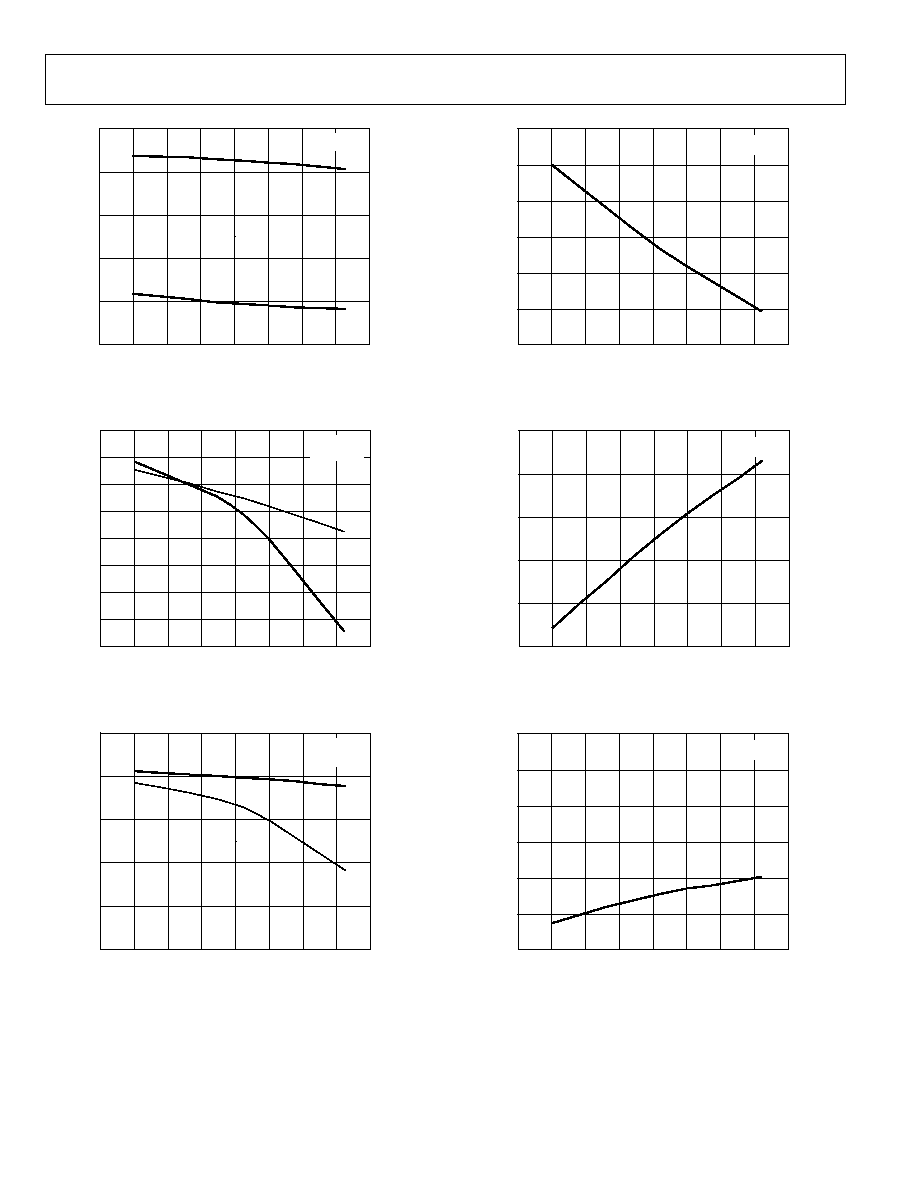
TYPICAL PERFORMANCE CHARACTERISTICS
0
10
20
30
40
50
NUMBE
R OF AMP
LIFIE
RS
60
70
80
0
0.2
0.4
0.6
0.8
1.0
1.2
TCV
OS
(
µV/°C)
04807-0-034
V
S
= ±15V
Figure 2. Input Offset Voltage Drift Distribution
0
10
20
30
40
50
NUMBE
R OF AMP
LIFIE
RS
60
70
80
100 80 60 40 20
0
40
80
20
60
100
V
OS
(
µV)
04807-0-058
V
S
= ±15V
Figure 3. Offset Voltage Distribution
0
10
20
30
40
50
60
70
NUMBE
R OF AMP
LIFIE
RS
400 320 240 160 80
0
160
320
80
240
400
I
B
(pA)
04807-0-060
V
S
= ±15V
Figure 4. Input Bias Distribution
40
20
0
20
40
60
80
100
GAIN (
d
B)
90
45
0
45
90
135
180
225
PH
A
SE M
A
R
G
IN
(
D
egrees)
FREQUENCY (Hz)
10k
1M
100k
10M
04807-0-001
V
S
= ±15V
Figure 5. Open-Loop Gain and Phase vs. Frequency
20
10
0
10
20
30
40
50
CLOSED-
L
OOP GAIN (
d
B)
FREQUENCY (Hz)
10k
1k
100k
1M
10M
04807-0-009
V
S
= ±15V
A
V
= 100
A
V
= 1
A
V
= 10
Figure 6. Closed-Loop Gain vs. Frequency
OUTP
UT IMP
E
DANCE
(
)
0
15
30
45
60
10
100
1k
10k
100k
1M
FREQUENCY (Hz)
04807-0-007
V
S
= ±15V
A
V
= 100
A
V
= 1
A
V
= 10
Figure 7. Output Impedance vs. Frequency
AD8698
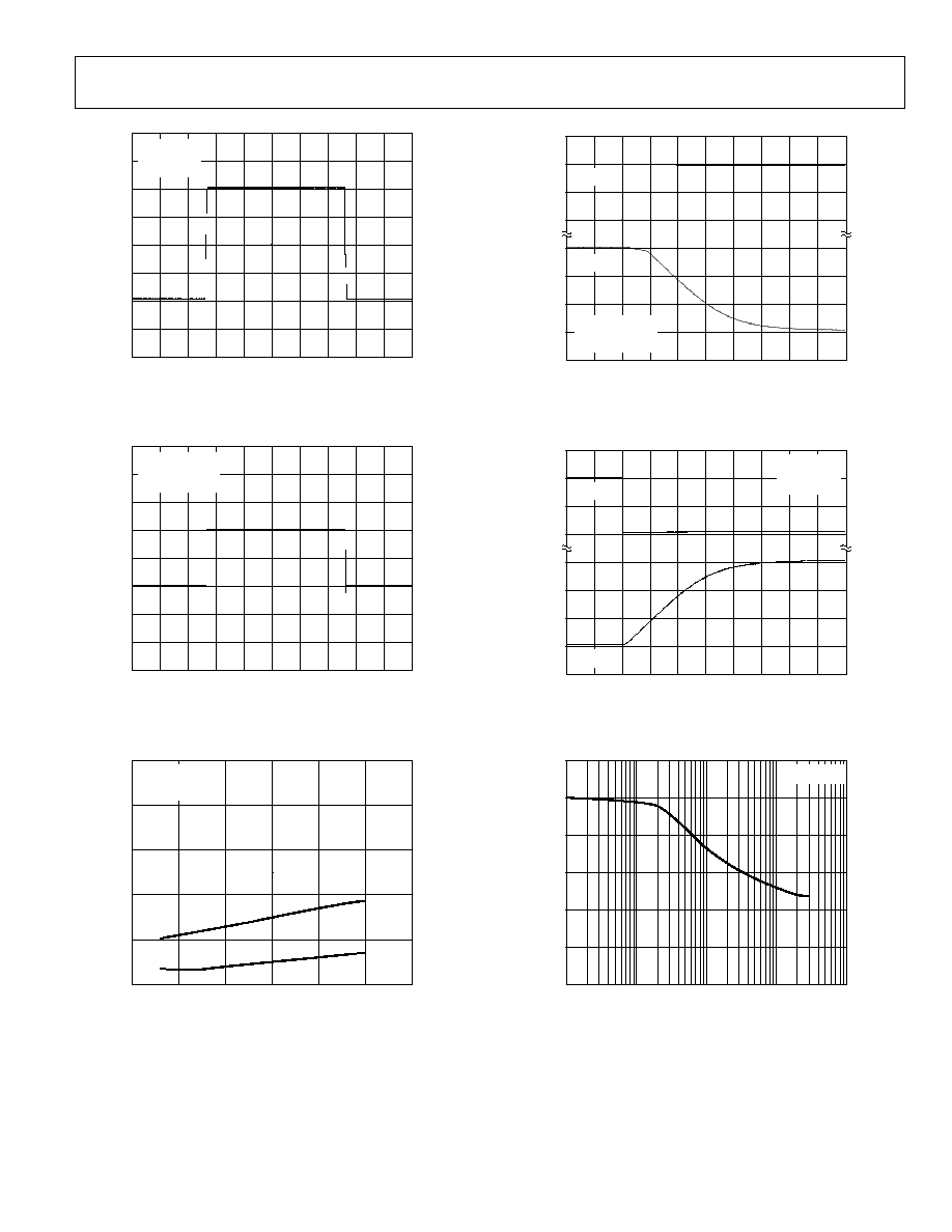
Rev. 0 | Page 7 of 20
VOLTA
GE (
1
V/D
IV)
V
S
= ±15V
V
IN
= 4V p-p
C
L
= 1nF
TIME (100
µs/DIV)
04807-0-037
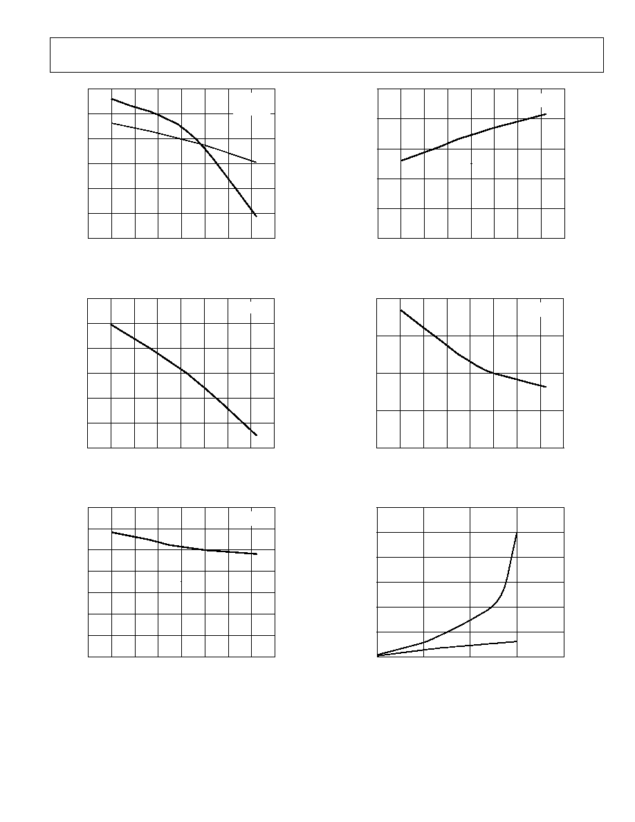
Figure 8. Large Signal Transient Response
VOLTA
GE (
100mV/D
IV)
V
S
= ±15V
V
IN
= 200mV p-p
C
L
= 1nF
TIME (100
µs/DIV)
04807-0-044
Figure 9. Small Signal Transient Response
0
10
20
30
50
OVER
SH
OOT (
%
)
V
S
= ±15V
V
IN
= 200mV
A
V
= 1
1000
1500
0
500
2000
2500
3000
CAPACITIVE LOAD (pF)
04807-0-013
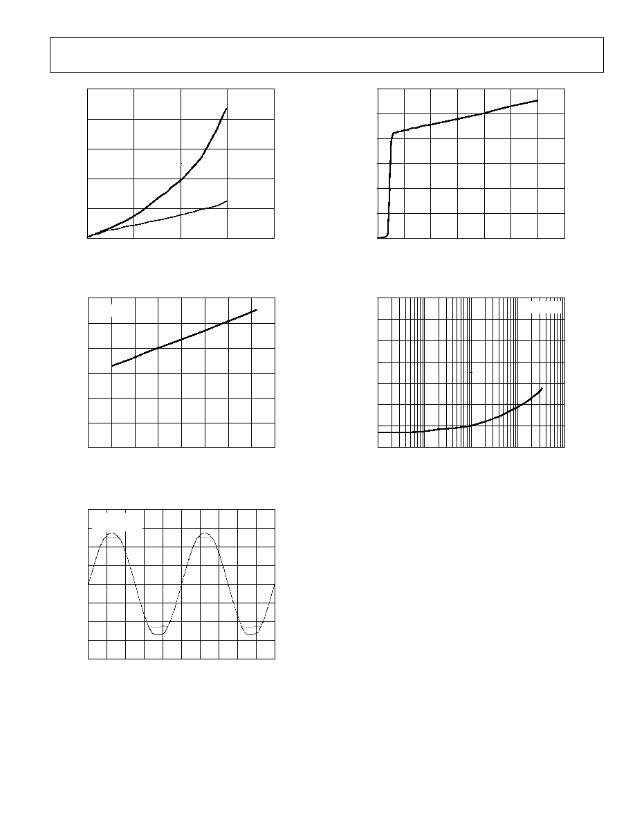
Figure 10. Overshoot vs. Load Capacitance
V
S
= ±15V
V
IN
= 200mV p-p
A
V
= 100
VOLTAGE (V)
V
OLTAGE (mV)
V
IN
200
0
0
15
V
OUT
TIME (10
µs/DIV)
04807-0-041
Figure 11. Positive Overvoltage Recovery
V
S
= ±15V
V
IN
= 200mV
A
V
= 100
TIME (400
µs/DIV)
04807-0-040
VOLTAGE (V)
V
OLTAGE (mV)
V
IN
0
200
15
0
V
OUT
Figure 12. Negative Overvoltage Recovery
0
20
40
60
80
100
120
CMRR (dB)
FREQUENCY (Hz)
10k
1k
100k
1M
10M
04807-0-003
V
S
= ±15V
Figure 13. CMRR vs. Frequency
AD8698
Rev. 0 | Page 8 of 20
0
20
40
60
80
100
10
100
1k
10k
100k
1M
FREQUENCY (Hz)
04807-0-005
V
S
= ±15V
+PSRR
PSRR
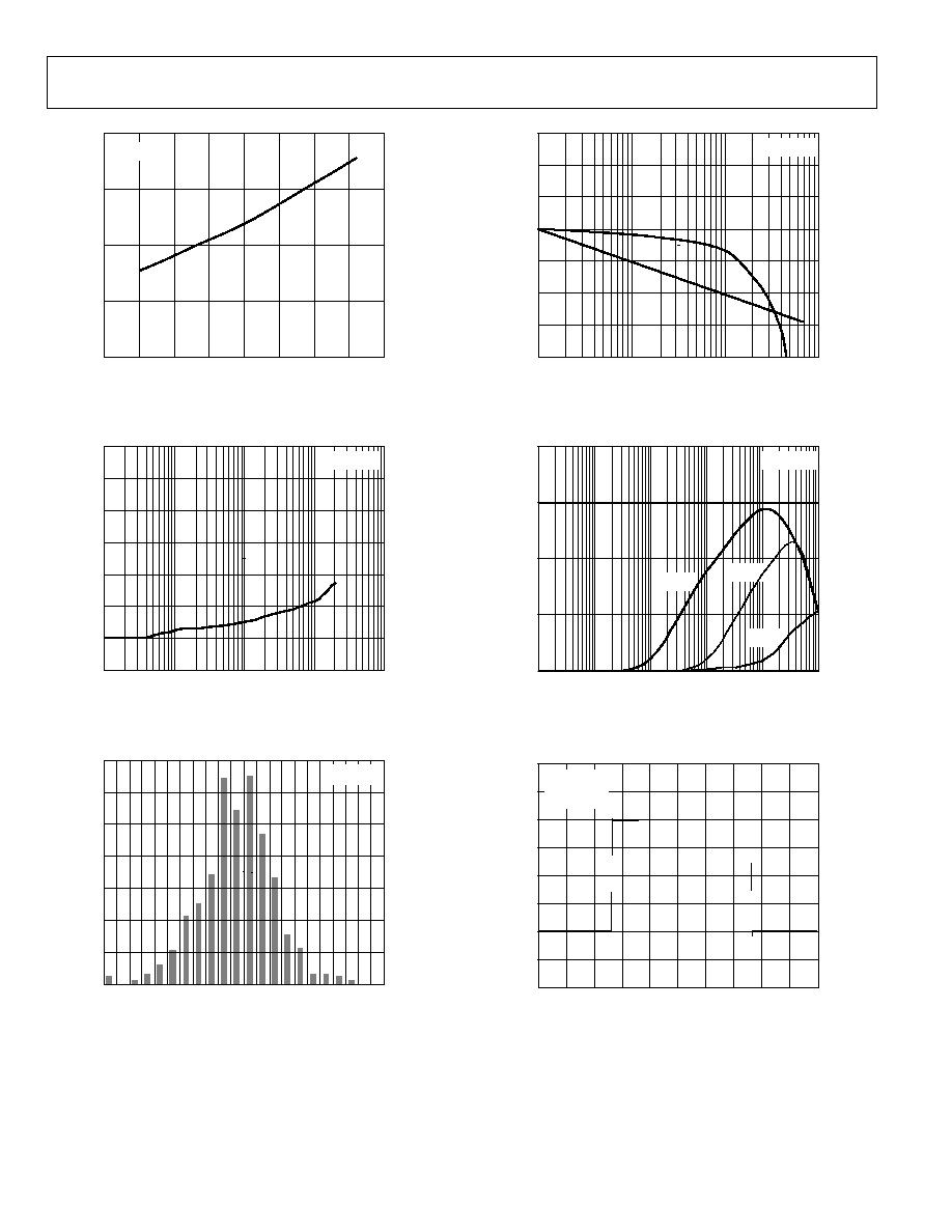
Figure 14. PSRR vs. Frequency
VOLTAGE (200nV/DIV)
V
S
= ±15V
TIME (1s/DIV)
04807-0-035
Figure 15. Input Voltage Noise
1
10
100
VOLTA
GE N
OISE D
E
N
S
ITY (
n
V/
Hz)
FREQUENCY (Hz)
1
0.1
10
100
1k
04807-0-032
V
S
= ±15V
Figure 16. Voltage Noise Density vs. Frequency
0.1
10
1
100
FREQUENCY (Hz)
1
0.1
10
100
1k
04807-0-033
V
S
= ±15V
CURRE
NT NOIS
E
DE
NS
ITY
(nV
/
Hz)
Figure 17. Current Noise Density vs. Frequency
40
30
20
10
0
10
20
S
H
ORT-CIRCUIT CURRE
NT (mA)
20
0
40
20
60
40
60
80
100
TEMPERATURE (°C)
04807-0-030
V
S
= ±15V
+I
SC
I
SC
Figure 18. Short-Circuit Current vs. Temperature
14.87
14.88
14.89
14.90
14.91
14.92
14.93
14.94
14.95
14.96
OUTPUT SW
ING (
V
)
20
0
40
20
60
40
60
80
100
TEMPERATURE (°C)
04807-0-019
V
S
= ±15V
I
L
= 1mA
V
OH
V
OL
Figure 19. Output Swing vs. Temperature
AD8698
Rev. 0 | Page 9 of 20
14.60
14.65
14.70
14.75
14.80
14.85
14.90
OUTPUT VOLTAGE SW
ING (
V
)
20
0
40
20
60
40
60
80
100
TEMPERATURE (°C)
04807-0-020
V
S
= ±15V
I
L
= 5mA
V
OH
V
OL
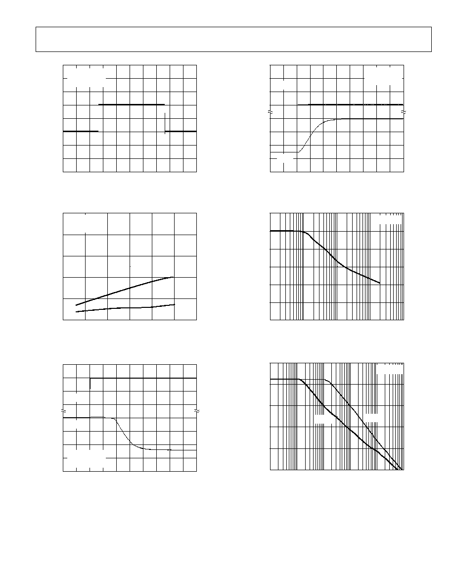
Figure 20. Output Voltage Swing vs. Temperature
30
20
10
0
10
20
30
OFFSET VOLTA
GE (
µ
V)
20
0
40
20
60
40
60
80
100
TEMPERATURE (°C)
04807-0-023
V
S
= ±15V
Figure 21.
Offset Voltage vs. Temperature
120
125
130
135
140
145
150
155
CMRR (dB)
20
0
40
20
60
40
60
80
100
TEMPERATURE (°C)
04807-0-027
V
S
= ±15V
Figure 22. CMRR vs. Temperature
130
132
134
136
138
140
P
S
RR (dB)
20
0
40
20
60
40
60
80
100
TEMPERATURE (°C)
04807-0-029
V
S
= ±15V
Figure 23. PSRR vs. Temperature
INP
U
T BIAS
CURRE
NT (pA)
100
50
0
50
100
20
0
40
20
60
40
60
80
100
TEMPERATURE (°C)
04807-0-025
V
S
= ±15V
Figure 24.
Input Bias Current vs. Temperature
0
1
2
3
4
5
6
OUTPUT SW
ING (
V
)
LOAD CURRENT (mA)
5
0
10
15
20
04807-0-015
V
S
= ±15V
V
OL
V
OH
Figure 25.
Output Voltage Swing from Rails vs. Load Current
AD8698
Rev. 0 | Page 10 of 20
S
U
P
P
L
Y
CURRE
NT (mA)
1.5
2.0
2.5
3.0
3.5
20
0
40
20
60
40
60
80
100
TEMPERATURE (°C)
04807-0-017
V
S
= ±15V
Figure 26. Supply Current vs. Temperature
140
120
100
80
60
40
20
0
CHANNE
L S
E
P
ARATION (dB)
FREQUENCY (Hz)
10k
1k
100k
1M
10M
04807-0-010
V
S
= ±15V
Figure 27. Channel Separation
0
10
20
30
40
50
60
70
NUMBE
R OF AMP
LIFIE
RS
100 80 60 40 20
0
40
80
20
60
100
V
OS
(
µV)
04807-0-059
V
S
= ±2.5V
Figure 28. Offset Voltage Distribution
40
20
0
20
40
60
80
100
GAIN (
d
B)
90
45
0
45
90
135
180
225
P
HAS
E
MARGIN (De
gre
e
s
)
FREQUENCY (Hz)
10k
1M
100k
10M
04807-0-002
V
S
= ±2.5V
Figure 29. Open-Loop Gain and Phase vs. Frequency
OUTP
UT IMP
E
DANCE
(
)
0
15
30
45
60
10
100
1k
10k
100k
1M
FREQUENCY (Hz)
04807-0-008
V
S
= ±2.5V
A
V
= 100
A
V
= 1
A
V
= 10
Figure 30. Output Impedance vs. Frequency
VOLTA
GE (
500mV/D
IV)
V
S
= ±2.5V
V
IN
= 2V p-p
C
L
= 1nF
0
TIME (100
µs/DIV)
04807-0-038
Figure 31. Large Signal Transient Response
AD8698
Rev. 0 | Page 11 of 20
VOLTAGE (
100mV/DIV)
V
S
= ±2.5V
V
IN
= 200mV p-p
C
L
= 1nF
TIME (100
µs/DIV)
04807-0-045
Figure 32. Small Signal Transient Response
0
10
20
30
40
50
OVER
SH
OOT (
%
)
V
S
= ±2.5V
V
IN
= 200mV
A
V
= 1
1000
1500
0
500
2000
2500
3000
CAPACITIVE LOAD (pF)
04807-0-014
Figure 33. Overshoot vs. Load Capacitance
V
S
= ±2.5V
V
IN
= 200mV p-p
A
V
= 100
TIME (4
µs/DIV)
04807-0-043
VOLTAGE (V)
V
OLTAGE (mV)
V
IN
200
0
0
2.5
V
OUT
Figure 34. Positive Overvoltage Recovery
V
S
= ±2.5V
V
IN
= 200mV p-p
A
V
= 100
TIME (4
µs/DIV)
04807-0-042
VOLTAGE (V)
V
OLTAGE (mV)
V
IN
0
200
2.5
0
V
OUT
Figure 35. Negative Overvoltage Recovery
0
20
40
60
80
100
120
CMRR (dB)
FREQUENCY (Hz)
10k
1k
100k
1M
10M
04807-0-004
V
S
= ±2.5V
Figure 36. CMRR vs. Frequency
0
20
40
60
80
100
P
S
RR (dB)
10
100
1k
10k
100k
1M
FREQUENCY (Hz)
04807-0-006
V
S
= ±2.5V
+PSRR
PSRR
Figure 37. PSRR vs. Frequency
AD8698
Rev. 0 | Page 12 of 20
30
20
10
0
10
20
S
H
ORT-CIRCUIT CURRE
NT (mA)
20
0
40
20
60
40
60
80
100
TEMPERATURE (°C)
04807-0-031
V
S
= ±2.5V
+I
SC
I
SC
Figure 38. Short-Circuit Current vs. Temperature
2.38
2.39
2.40
2.41
2.42
2.43
OUTPUT VOLTAGE (V)
2.44
2.45
2.46
20
0
40
20
60
40
60
80
100
TEMPERATURE (°C)
04807-0-021
V
S
= ±2.5V
I
L
= 1mA
V
OH
V
OL
Figure 39. Output Swing vs. Temperature
1.5
1.7
1.9
2.1
2.3
2.5
OUTPUT VOLTAGE SW
ING (
V
)
20
0
40
20
60
40
60
80
100
TEMPERATURE (°C)
04807-0-022
V
S
= ±2.5V
I
L
= 5mA
V
OH
V
OL
Figure 40. Output Voltage Swing vs. Temperature
30
20
10
0
10
20
30
OFFSET VOLTA
GE (
µ
V)
20
0
40
20
60
40
60
80
100
TEMPERATURE (°C)
04807-0-024
V
S
= ±2.5V
Figure 41.
Offset Voltage vs. Temperature
124
126
128
130
132
134
CMRR (dB)
20
0
40
20
60
40
60
80
100
TEMPERATURE (°C)
04807-0-028
V
S
= ±2.5V
Figure 42. CMRR vs. Temperature
80
70
60
50
40
30
20
INP
U
T OFFS
E
T CURRE
NT (pA)
20
0
40
20
60
40
60
80
100
TEMPERATURE (°C)
04807-0-026
V
S
= ±2.5V
Figure 43.
Input Bias Current vs. Temperature
AD8698
Rev. 0 | Page 13 of 20
0
500
1000
1500
2000
2500
OUTPUT SW
ING (
mV)
LOAD CURRENT (mA)
5
0
10
15
20
04807-0-016
V
S
= ±2.5V
V
OH
V
OL
Figure 44.
Output Voltage Swing from Rails vs. Load Current
0
0.5
1.0
1.5
2.0
2.5
3.0
S
U
P
P
L
Y
CURRE
NT (mA)
20
0
40
20
60
40
60
80
100
TEMPERATURE (°C)
04807-0-018
V
S
= ±2.5V
Figure 45. Supply Current vs. Temperature
VOLTA
GE (
2
V/D
IV)
V
S
= ±5V
V
IN
= 11.4V p-p
TIME (400
µs/DIV)
04807-0-039
Figure 46. No Phase Reversal
0
0.5
1.0
1.5
2.0
2.5
3.0
S
U
P
P
LY
CURRE
NT (mA)
0
5
10
15
20
25
30
35
SUPPLY VOLTAGE (V)
04807-0-012
Figure 47. Supply Current vs. Supply Voltage
140
120
100
80
60
40
20
0
CHANNE
L S
E
P
ARATION (dB)
FREQUENCY (Hz)
10k
1k
100k
1M
10M
04807-0-011
V
S
= ±2.5V
Figure 48. Channel Separation
AD8698
Rev. 0 | Page 14 of 20
APPLICATIONS
INPUT OVERVOLTAGE PROTECTION
The AD8698 has internal protective circuitry which allows
voltages at either input to exceed the supply voltage. However,
if voltages applied at either input exceed the supply voltage by
more than 2 V, it is recommended to use a resistor in series
with the inputs to limit the input current and prevent damaging
the device.
The value of the resistor can be calculated from the following
formula:
mA
5
500
+
-
S
S
IN
R
V
V
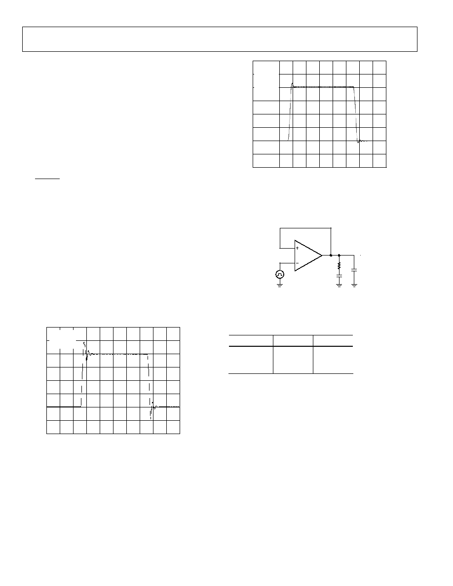
DRIVING CAPACITIVE LOADS
The AD8698 is stable even when driving heavy capacitive
loads in any configuration. Although the AD8698 will safely
drive capacitive loads well over 10 nF, it is recommended to
use external compensation should the amplifier be subjected
to driving a load exceeding 50 nF. This is particularly
important in positive unity gain configurations, the worst
case for stability.
Figure
49 shows the output of the AD8698
with a 68 nF load in response to a 400 mV signal at its
positive input; the overshoot is less than 25% without any
external compensation. Using a simple "snubber" network
reduces the overshoot to less than 10% as shown in
Figure
50.
VOLTA
GE (
100mV/D
IV)
V
S
= ±15V
C
L
= 68nF
A
V
= 1
TIME (10
µs/DIV)
04807-0-057.
Figure 49. Heavy Capacitive Load Drive without Compensation
VOLTA
GE (
100mV/D
IV)
V
S
= ±15V
C
L
= 68nF
R
S
= 30
C
S
= 5nF
A
V
= 1
TIME (10
µs/DIV)
04807-0-061
Figure 50. Compensated Capacitive Load Drive with Snubber
The snubber network consists of a simple RC network
whose values are determined empirically.
V+
R
S
C
S
C
L
V
400mV
+
04807-0-063
Figure 51. Snubber Network
Table 5
provides a few starting values for optimum
compensation.
Table 5. Compensation Values
C
L
(nF)
R
S
(
)
C
S
(nF)
47 20
7
68 30
5
100 50 3
The use of the snubber network does not recover the loss of
bandwidth incurred by the load capacitance. The AD8698
maintains a unity gain bandwidth of 1 MHz with load
capacitances of up to 1 nF.
AD8698
Rev. 0 | Page 15 of 20
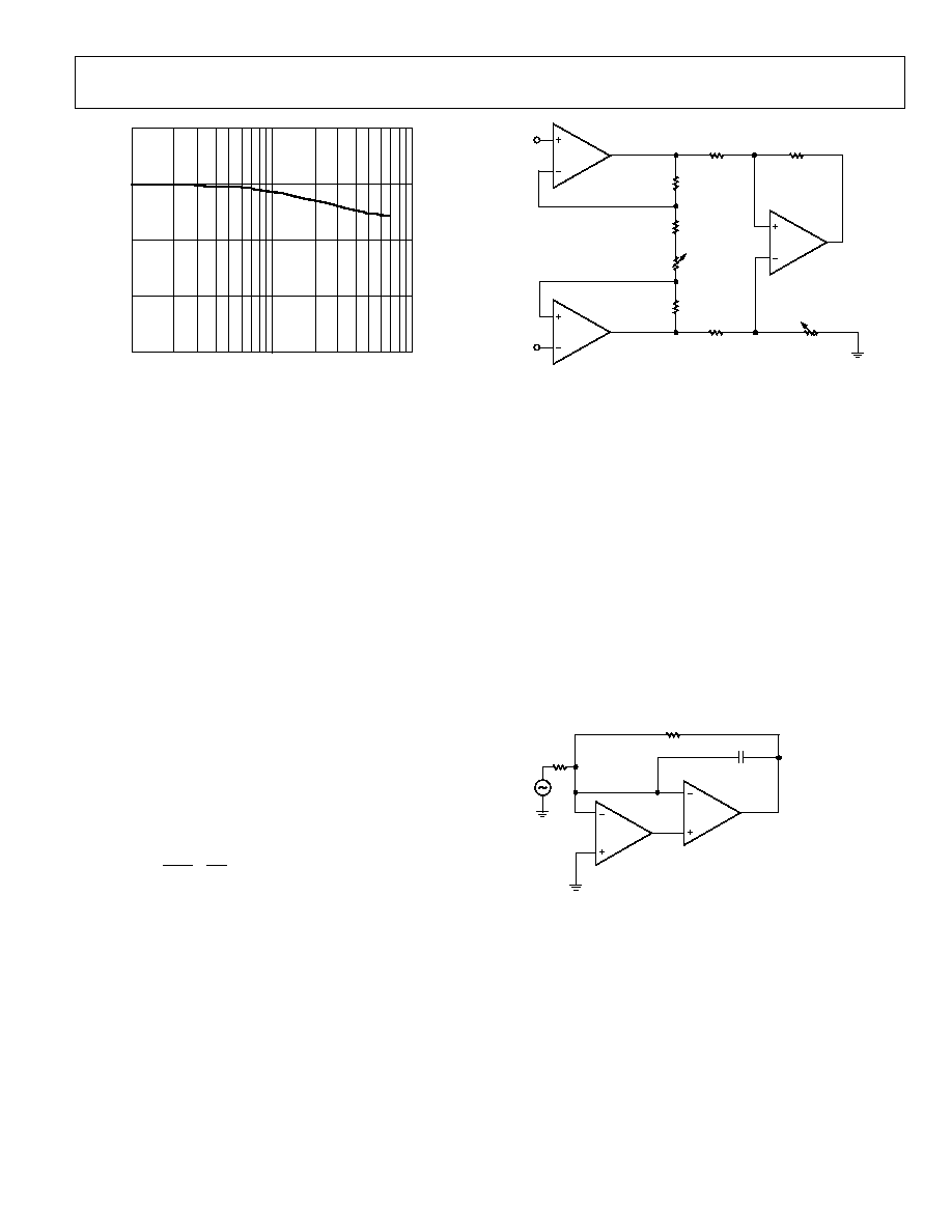
UNITY
GAIN BANDWIDTH (MHz)
1k
10k
100k
1M
10M
LOAD CAPACITANCE (nF)
1
10
100
04807-0-062
Figure 52. Unity Gain Bandwidth vs. Load Capacitance
Figure 52 shows the unity gain bandwidth as a function of load
capacitance.
INSTRUMENTATION AMPLIFIER
Instrumentation amplifiers are used in applications requiring
precision, accuracy, and high CMRR. One popular application
is signal conditioning in process control, test automation, and
measurement instrumentation, where the amplifier is used to
amplify small signals.
The triple op amp implementation uses the AD8698 at the
front end with the OP184 for optimum accuracy.
The circuit in Figure 53 enjoys a high overall gain, excellent dc
performance, high CMRR, as well as the benefit of an output
that swings to the supplies.
The CMRR of the in-amp will be limited by the choice of
resistor tolerance. R5 is an optional potentiometer that can be
used to calibrate the circuit for maximum gain. R7 can be
trimmed for optimum CMRR.
The output voltage is given by:
+
=
1
R
2
R
4
R
3
R
V
V
IN
O
2
1
V
V+
V+
R3
9k
R1
1k
R2
10k
R1
9.8k
R7
400
R4
2k
R5
10k
R3
9k
V
V2
V1
04807-0-064
V
V+
OP184
1/2 AD8698
1/2 AD8698
Figure 53. Three Op Amp In-Amp
COMPOSITE AMPLIFIER
The dc accuracy of the AD8698 and the ac performance of the
OP184 are combined in the circuit shown in Figure 54. The
composite amplifier provides a higher bandwidth, a lower offset
voltage, and a higher loop, thereby reducing the gain error
substantially.
The circuit shown exhibits a total output rms noise of less than
500 µV, corresponding to less than 3 mV of peak-to-peak noise
over approximately a 3 MHz bandwidth. Cf is used to minimize
peaking.
The circuit has an inverting gain of 10. In applications with
higher closed-loop gains, Cf is necessary to maintain a
sufficient phase margin and ensure stability. This results in a
narrower closed-loop bandwidth.
V+
OP184
1/2 AD8698
V
V+
V
04807-0-065
R2
10k
R1
1k
Cf
20pF
V
IN
Figure 54. Composite Amplifier Circuit
AD8698
Rev. 0 | Page 16 of 20
LOW NOISE APPLICATIONS
In some applications, it is critical to minimize the noise, and
although the AD8698 has a low noise of typically 8 nV/Hz at
1 kHz, paralleling the two amplifiers within the same package
reduces the total noise referred to the input to approximately
5.5 nV/Hz. This simple technique is depicted in Figure 55.
V
V+
V+
R4
10k
V
04807-0-066
R2
10k
V
OUT
V
IN
R3
1k
R1
1k
R5
100
R3
100
Figure 55. Paralleling Amplifiers
DRIVING ADCs
The AD8698 can drive extremely heavy capacitive loads
without any compensation. Sometimes capacitors are placed at
the output of the amplifier to absorb transient currents while
the op amp is interfaced with the ADC. Most op amps need a
small resistor with the output to isolate the load capacitance.
This results in a loss of bandwidth and slows the amplifier
down substantially. However, the AD8698 maintains a unity
gain bandwidth of 1 MHz with loads of up to 1 nF, as shown in
Figure 52.
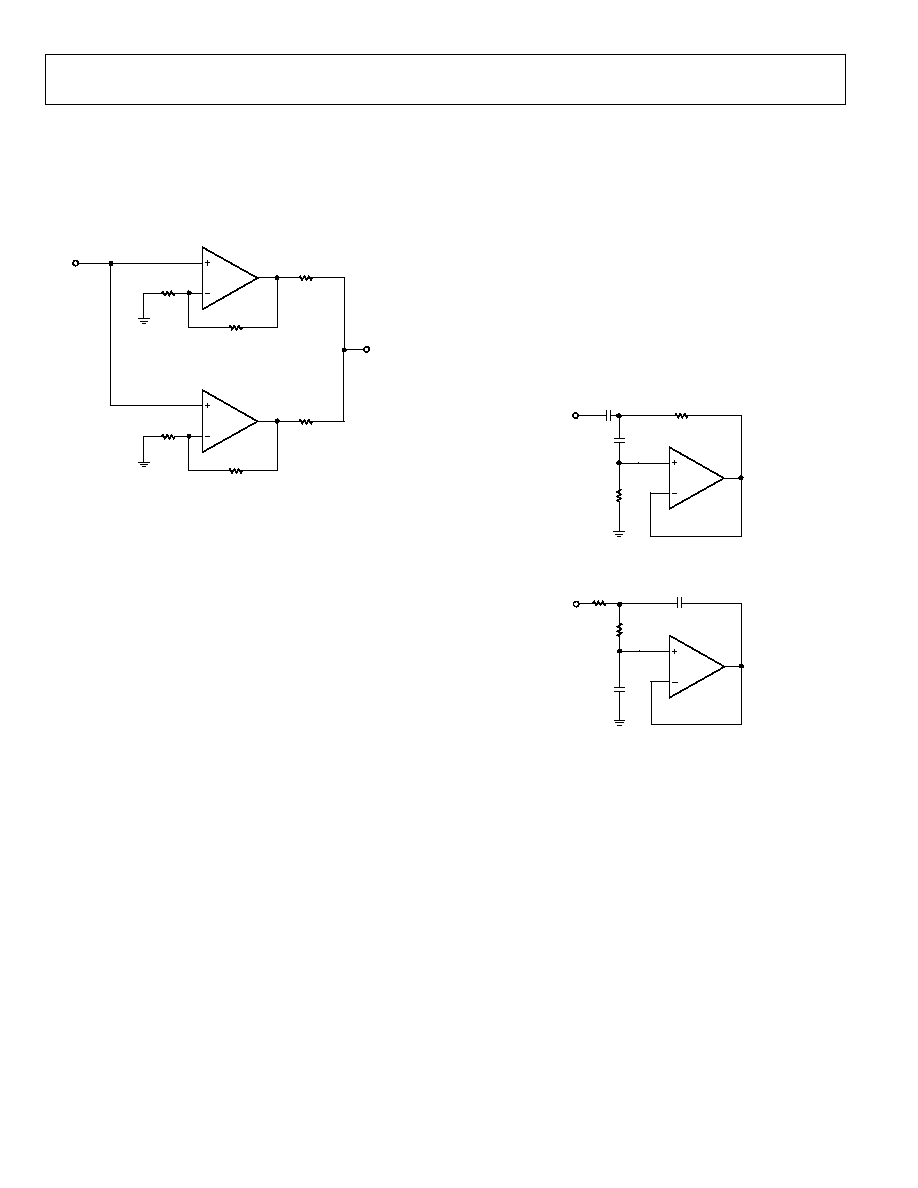
USING THE AD8698 IN ACTIVE FILTER DESIGNS
The AD8698 is recommended for unity gain filter designs with
a corner frequency of up to 100 kHz, one tenth of the op amp's
unity gain bandwidth.
If a higher gain is desired, the corner frequency should be
chosen accordingly. For example, if the amplifier is configured
with a gain of 10, the corner frequency of the filter should not
be more than 10 kHz.
An example of an active filter is the Sallen Key. This topology
gives the user the flexibility of implementing a low-pass or a
high-pass filter by simply interchanging the resistors and the
capacitors.
In the high-pass filter of Figure 56, the damping factor Q is set
to 1/2 for a maximally flat response (Butterworth).
The gain is unity and the bandwidth is 10 kHz with the values
shown.
V
V+
04807-0-067
R2
22k
R1
11k
C1
1nF
C2
1nF
V
IN
Figure 56. Two Pole High-Pass Filter
V
V+
04807-0-068
R2
11k
R1
11k
C1
2nF
C2
1nF
VIN
Figure 57. Two Pole Low-Pass Filter
The circuit of Figure 57 has a bandwidth of 10 kHz and a
maximally flat response. In this case, the damping factor is
controlled by the ratio of the capacitors and the gain is unity.
AD8698
Rev. 0 | Page 17 of 20
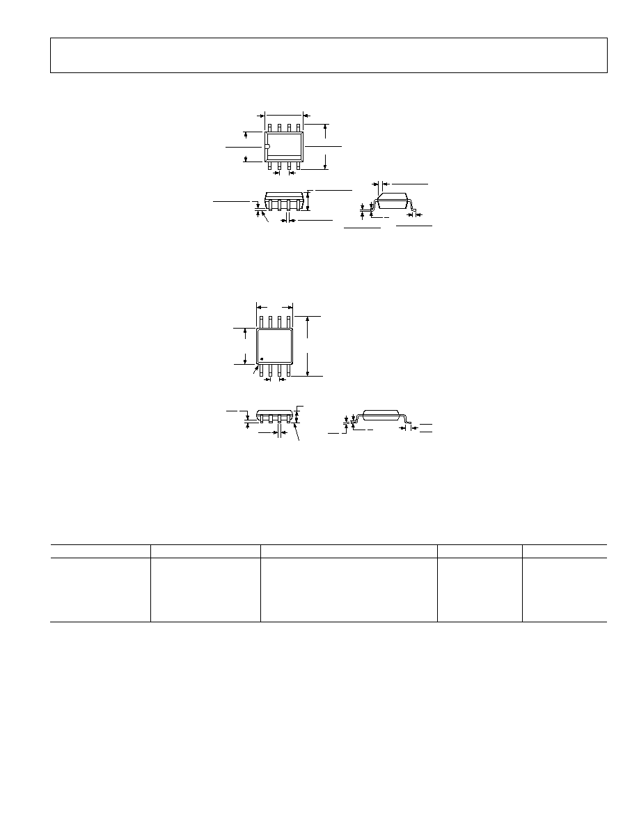
OUTLINE DIMENSIONS
0.25 (0.0098)
0.17 (0.0067)
1.27 (0.0500)
0.40 (0.0157)
0.50 (0.0196)
0.25 (0.0099)
× 45°
8°
0°
1.75 (0.0688)
1.35 (0.0532)
SEATING
PLANE
0.25 (0.0098)
0.10 (0.0040)
4
1
8
5
5.00 (0.1968)
4.80 (0.1890)
4.00 (0.1574)
3.80 (0.1497)
1.27 (0.0500)
BSC
6.20 (0.2440)
5.80 (0.2284)
0.51 (0.0201)
0.31 (0.0122)
COPLANARITY
0.10
CONTROLLING DIMENSIONS ARE IN MILLIMETERS; INCH DIMENSIONS
(IN PARENTHESES) ARE ROUNDED-OFF MILLIMETER EQUIVALENTS FOR
REFERENCE ONLY AND ARE NOT APPROPRIATE FOR USE IN DESIGN
COMPLIANT TO JEDEC STANDARDS MS-012AA
Figure 58. 8-Lead Small Outline IC [SOIC] (R-8)--Dimensions shown in millimeters
0.80
0.60
0.40
8°
0°
4
8
5
4.90
BSC
PIN 1
0.65 BSC
3.00
BSC
SEATING
PLANE
0.15
0.00
0.38
0.22
1.10 MAX
3.00
BSC
COPLANARITY
0.10
0.23
0.08
COMPLIANT TO JEDEC STANDARDS MO-187AA
Figure 59. 8-Lead Small Outline IC [SOIC] (RM-8)--Dimensions shown in millimeters
ORDERING GUIDE
Model Temperature
Package
Package
Description
Package Option
Branding
AD8698ARM-R2
40°C to +85°C
MSOP
RM-8
A02
AD8698ARM-REEL
40°C to +85°C
MSOP
RM-8
A02
AD8698AR
40°C to +85°C
SOIC
R-8
AD8698AR-REEL
40°C to +85°C
SOIC
R-8
AD8698AR-REEL7
40°C to +85°C
SOIC
R-8

AD8698
Rev. 0 | Page 18 of 20
NOTES

AD8698
Rev. 0 | Page 19 of 20
NOTES

AD8698
Rev. 0 | Page 20 of 20
NOTES
© 2004 Analog Devices, Inc. All rights reserved. Trademarks and
registered trademarks are the property of their respective owners.
D04807-0-4/04(0)
Document Outline
- FEATURES
- APPLICATIONS
- GENERAL DESCRIPTION
- SPECIFICATIONS
- þÿ
- þÿ
- þÿ
- þÿ