
REV. B
Information furnished by Analog Devices is believed to be accurate and
reliable. However, no responsibility is assumed by Analog Devices for its
use, nor for any infringements of patents or other rights of third parties
which may result from its use. No license is granted by implication or
otherwise under any patent or patent rights of Analog Devices.
a
10-Bit 40 MSPS
A/D Converter
AD9040A
FEATURES
Low Power: 940 mW
53 dB SNR @ 10 MHz A
IN
On-Chip T/H, Reference
CMOS-Compatible
2 V p-p Analog Input
Fully Characterized Dynamic Performance
APPLICATIONS
Ultrasound Medical Imaging
Digital Oscilloscopes
Professional Video
Digital Communications
Advanced Television (MUSE Decoders)
Instrumentation
GENERAL DESCRIPTION
The AD9040A is a complete 10-bit monolithic sampling analog-
to-digital converter (ADC) with on-board track-and-hold and
reference. The unit is designed for low cost, high performance
applications and requires only an encode signal to achieve
40 MSPS sample rates with 10-bit resolution.
Digital inputs and outputs are CMOS compatible; the analog
input requires a signal of 2 V p-p amplitude. The two-step
architecture used in the AD9040A is optimized to provide the
best dynamic performance available while maintaining low
power requirements of only 940 mW typically; maximum dissi-
pation is 1.1 watt at 40 MSPS.
The signal-to-noise ratio (SNR), including harmonics, is 53 dB,
or 8.5 ENOB, when sampling an analog input of 10.3 MHz at
40 MSPS. Competitive devices perform at less than 7.5 ENOB
and require external references and larger input signals.
The AD9040A A/D converter is available as either a 28-lead
plastic DIP or a 28-lead SOIC. The two models operate over a
commercial temperature range of 0
�
C to +70
�
C. Contact the
factory regarding availability of ceramic military temperature
range devices.
FUNCTIONAL BLOCK DIAGRAM
ERROR
CORRECTION
AD9040A
10
BANDGAP
REFERENCE
6-BIT
ADC
5-BIT
ADC
T/H
T/H
DECODE
LOGIC
DECODE
LOGIC
ENCODE
A
IN
GND
V
OUT
V
REF
BP
REF
AMP
ARRAY
REF
AMP
PRODUCT HIGHLIGHTS
1. CMOS compatible logic for direct interface to ASICs.
2. On-board T/H provides excellent high frequency perfor-
mance on analog inputs, critical for communications and
medical imaging applications.
3. High input impedance and 2 volt p-p input range reduce
need for external amplifiers.
4. Easy to use; no cumbersome external voltage references
required, allowing denser packing of ADCs for multichannel
applications.
5. Available in 28-lead plastic DIP and SOIC packages.
6. Evaluation board includes AD9040AJR, reconstruction
DAC, and latches. Space is available near the analog input
and digital outputs of the converter for additional circuits.
Order as part number AD9040A/PCB (schematic shown in
data sheet).
One Technology Way, P.O. Box 9106, Norwood, MA 02062-9106, U.S.A.
Tel: 781/329-4700
World Wide Web Site: http://www.analog.com
Fax: 781/326-8703
� Analog Devices, Inc., 1999

AD9040A�SPECIFICATIONS
ELECTRICAL CHARACTERISTICS
Test
AD9040AJN/JR
Parameter (Conditions)
Temp
Level
Min
Typ
Max
Units
RESOLUTION
10
Bits
DC ACCURACY
Differential Nonlinearity
+25
�
C
I
1.0
2.0
LSB
Full
VI
2.5
LSB
Integral Nonlinearity
+25
�
C
I
1.0
2.0
LSB
Full
VI
2.5
LSB
No Missing Codes
Full
VI
Guaranteed
Gain Error
+25
�
C
I
�
0.5
�
1.5
% FS
Full
VI
�
2
% FS
Gain Tempco
1
Full
V
�
70
ppm/
�
C
ANALOG INPUT
Input Voltage Range
+25
�
C
V
2
V p-p
Input Offset Voltage
+25
�
C
I
�
2
�
25
mV
Full
VI
�
30
mV
Input Bias Current
+25
�
C
I
7
15
�
A
Full
VI
25
�
A
Input Resistance
+25
�
C
I
200
350
k
Input Capacitance
+25
�
C
V
5
pF
Analog Bandwidth
+25
�
C
V
48
MHz
BANDGAP REFERENCE
Output Voltage
Full
VI
2.4
2.6
V
Temperature Coefficient
1
Full
V
�
40
ppm/
�
C
SWITCHING PERFORMANCE
Maximum Conversion Rate
+25
�
C
I
40
MSPS
Minimum Conversion Rate
+25
�
C
IV
2
10
MSPS
Aperture Delay (t
A
)
+25
�
C
V
1.9
ns
Aperture Uncertainty (Jitter)
+25
�
C
V
7
ps, rms
Output Propagation Delay (t
PD
)
2
+25
�
C
I
7.5
10
12
ns
Full
IV
6
14
ns
DYNAMIC PERFORMANCE
Transient Response
+25
�
C
V
25
ns
Overvoltage Recovery Time
+25
�
C
V
40
ns
Signal-to-Noise Ratio
3
f
IN
= 2.3 MHz
+25
�
C
I
51
54
dB
f
IN
= 10.3 MHz
+25
�
C
I
50
53
dB
Signal-to-Noise Ratio
3
(Without Harmonics)
f
IN
= 2.3 MHz
+25
�
C
I
52
55
dB
f
IN
= 10.3 MHz
+25
�
C
I
51
54
dB
Signal-to-Noise Ratio
3, 4
f
IN
= = 2.3 MHz
+25
�
C
I
52
56
dB
f
IN
= = 10.3 MHz
+25
�
C
I
51
55
dB
Signal-to-Noise Ratio
3, 4
(Without Harmonics)
f
IN
= 2.3 MHz
+25
�
C
I
53
57
dB
f
IN
= 10.3 MHz
+25
�
C
I
53
56
dB
2nd Harmonic Distortion
f
IN
= 2.3 MHz
+25
�
C
I
56
67
dBc
f
IN
= 10.3 MHz
+25
�
C
I
56
65
dBc
3rd Harmonic Distortion
f
IN
= 2.3 MHz
+25
�
C
I
58
73
dBc
f
IN
= 10.3 MHz
+25
�
C
I
58
70
dBc
Two-Tone Intermodulation
+25
�
C
V
62
dBc
Distortion Rejections
Differential Phase
+25
�
C
III
0.15
0.5
Degrees
Differential Gain
+25
�
C
III
0.25
1.0
%
REV. B
�2�
(+V
S
= V
D
= +5 V; �V
S
= �5 V; internal reference: ENCODE = 40.5 MSPS unless
otherwise noted)

AD9040A
REV. B
�3�
Test
AD9040AJN/JR
Parameter (Conditions)
Temp
Level
Min
Typ
Max
Units
ENCODE INPUT
Logic "1" Voltage
Full
VI
4.0
V
Logic "0" Voltage
Full
VI
1.0
V
Logic "1" Current
Full
VI
�
1
�
A
Logic "0" Current
Full
VI
�
1
�
A
Input Capacitance
+25
�
C
V
14
pF
Encode Pulsewidth (High) (t
EH
)
6
+25
�
C
IV
10
100
ns
Encode Pulsewidth (Low) (t
EL
)
6
+25
�
C
IV
10
100
ns
DIGITAL OUTPUTS
Logic "1" Voltage
Full
VI
4.95
V
Logic "0" Voltage
Full
VI
0.05
V
Output Coding
Offset Binary
POWER SUPPLY
V
D
Supply Current
Full
VI
13
20
mA
+V
S
Supply Current
Full
VI
89
110
mA
�V
S
Supply Current
Full
VI
87
105
mA
Power Dissipation
Full
VI
0.94
1.2
W
Power Supply
Rejection Ratio (PSRR)
7
+25
�
C
I
�
15
mV/V
NOTES
1
"Gain Tempco" is for converter using internal reference; "Temperature
Coefficient" is for bandgap reference only.
2
Output propagation delay (t
PD
) is measured from the 50% point of the falling
edge of the encode command to the min/max voltage levels of the digital
outputs with 10 pF maximum loads.
3
RMS signal to rms noise with analog input signal 1 dB below full scale at
specified frequency.
4
ENCODE = 32 MSPS.
5
3rd order intermodulation measured with analog input frequencies of 2.3 MHz
and 2.4 MHz at 7 dB below full scale.
6
For rated performance at 40 MSPS, duty cycle of encode command should be
50%
�
10%.
7
Measured as the ratio of the change in offset voltage for a 5% change in +V
S
or �V
S
.
Specifications subject to change without notice.
EXPLANATION OF TEST LEVELS
Test Level
I
� 100% Production Tested.
II � 100% production tested at +25
�
C, and sample tested at
specified temperatures. AC testing done on sample basis.
III � Sample Tested Only.
IV � Parameter is guaranteed by design and characterization
testing.
V � Parameter is a typical value only.
VI � All devices are 100% production tested at +25
�
C. 100%
production tested at temperature extremes for military
temperature devices; guaranteed by design and character-
ization testing for industrial devices.
ABSOLUTE MAXIMUM RATINGS
1
�
V
S
. . . . . . . . . . . . . . . . . . . . . . . . . . . . . . . . . . . . . . . . . .
�
7 V
V
D
. . . . . . . . . . . . . . . . . . . . . . . . . . . . . . . . . . . . . . . . . . . +7 V
ANALOG IN . . . . . . . . . . . . . . . . . . . . . . . . . . . . �V
S
to +V
S
DIGITAL INPUTS . . . . . . . . . . . . . . . . . . . . . . . . . 0 V to +V
S
V
REF
Input . . . . . . . . . . . . . . . . . . . . . . . . . . . . . . . . 0 V to +V
S
Digital Output Current . . . . . . . . . . . . . . . . . . . . . . . . . 20 mA
Operating Temperature
AD9040AJN/JR . . . . . . . . . . . . . . . . . . . . . . . . 0
�
C to +70
�
C
Storage Temperature . . . . . . . . . . . . . . . . . �65
�
C to +150
�
C
Maximum Junction Temperature
2
(JN/JR Suffixes) . . . +150
�
C
Lead Soldering Temp (10 sec) . . . . . . . . . . . . . . . . . . . +300
�
C
NOTES
1
Absolute maximum ratings are limiting values to be applied individually, and
beyond which the serviceability of the circuit may be impaired. Functional
operability is not necessarily implied. Exposure to absolute maximum rating
conditions for an extended period of time may affect device reliability.
2
Typical thermal impedances (parts soldered to board):
N Package (Plastic DIP):
JA
= 42
�
C/W;
JC
= 10
�
C/W.
R Package (SOIC):
JA
= 47
�
C/W;
JC
= 10
�
C/W.
ORDERING GUIDE
Model
Temperature Range
Package Description
Package Option
AD9040AJN
0
�
C to +70
�
C
28-Lead Plastic DIP
N-28
AD9040AJR
0
�
C to +70
�
C
28-Lead SOIC Package
R-28
AD9040A/PWB
Printed Circuit Board (Only) of Evaluation Circuit
AD9040A/PCB
Complete Evaluation Board, Assembled and Tested,
Including AD9040AJR
AD9040A
REV. B
�4�
PIN FUNCTION DESCRIPTIONS
Pin No.
Name
Function
1, 12, 21
�V
S
5 V Power Supply
2, 4, 11, 14, 22
GND
Ground
3, 10
+V
S
Analog +5 V Power Supply
5
V
OUT
Internal Bandgap Voltage
Reference (Nominally +2.5 V)
6
V
REF
Noninverting Input to Reference
Amplifier. Voltage reference for
ADC is connected here.
7
BP
REF
External Connection for (0.1
�
F)
Reference Bypass Capacitor
8
NC
No Connection Internally
9
ENCODE Encode Clock Input to ADC.
Internal T/H placed in hold mode
(ADC is encoding) on rising edge.
13
A
IN
Noninverting Input to T/H
Amplifier
15
OR
Out-of-Range Condition Output.
Active high when analog input
exceeds input range of ADC by
1 LSB (<FS �1 LSB or >+FS
+ 1 LSB).
16
D9 (MSB) Most Significant Bit of ADC
Output; TTL/CMOS Compatible
17�20
D8�D5
Digital Output Bits of ADC; TTL/
CMOS Compatible
23
V
D
Digital +5 V Power Supply
24�27
D4�D1
Digital Output Bits of ADC;
TTL/CMOSL Compatible
28
D0 (LSB)
Least Significant Bit of ADC
Output; TTL/CMOS Compatible
TOP VIEW
(Not to Scale)
28
27
26
25
24
23
22
21
20
19
18
17
16
15
1
2
3
4
5
6
7
8
9
10
11
12
13
14
AD9040A
NC = NO CONNECT
GND
A
IN
�V
S
GND
+V
S
ENCODE
NC
�V
S
GND
+V
S
GND
BP
REF
V
REF
V
OUT
OR
D9 (MSB)
D8
D7
D6
D5
�V
S
D0 (LSB)
D1
D2
D3
GND
V
D
D4
PDIP and SOIC Pinouts
ENCODE
GND
+V
S
V
REF
V
OUT
D1
D0 (LSB)
GND
+V
S
�V
S
D9 (MSB)
D8
OR
GND
GND
A
IN
�V
S
NC
BP
REF
D7
D6
D5
D4
D3
D2
DGND
�V
S
V
D
DIE LAYOUT AND MECHANICAL INFORMATION
Die Dimensions . . . . . . . . . . . . . . . . . 204
�
185
�
21 (
�
1) mils
Pad Dimensions . . . . . . . . . . . . . . . . . . . . . . . . . . . . . 4
�
4 mils
Metalization . . . . . . . . . . . . . . . . . . . . . . . . . . . . . . . Aluminum
Backing . . . . . . . . . . . . . . . . . . . . . . . . . . . . . . . . . . . . . . None
Substrate Potential . . . . . . . . . . . . . . . . . . . . . . . . . . . . . . .�V
S
Transistor Count . . . . . . . . . . . . . . . . . . . . . . . . . . . . . . . 5,070
Passivation . . . . . . . . . . . . . . . . . . . . . . . . . . . . . . . . Oxynitride
Die Attach (JN/JR) . . . . . . . . . . . . . . . . . . . . . . . . . . . . Epoxy
Bond Wire (JN/JR) . . . . . . . . . . . . . . . . . . . . . . . . . . . . . Gold
N
N + 1
#2
#3
ENCODE
N � 3
N � 2
N � 1
t
A
t
EH
t
EL
t
PD
A
IN
DIGITAL
OUTPUTS
APERTURE DELAY
PULSEWIDTH HIGH
PULSEWIDTH LOW
OUTPUT PROP DELAY
t
A
t
EH
t
EL
t
PD
1.9
10ns
10
7.5
100
12
MIN
TYP
MAX
10
100
Figure 1. Timing Diagram

AD9040A
REV. B
�5�
DEFINITIONS OF SPECIFICATIONS
Analog Bandwidth
The analog input frequency at which the spectral power of the
fundamental frequency (as determined by FFT analysis) is
reduced by 3 dB.
Aperture Delay
The delay between the rising edge of the ENCODE command
and the instant at which the analog input is sampled.
Aperture Uncertainty (Jitter)
The sample-to-sample variation in aperture delay.
Differential Gain
The percentage of amplitude change of a small high frequency
sine wave (3.58 MHz) superimposed on a low frequency signal
(15.734 kHz).
Differential Nonlinearity
The deviation of any code from an ideal 1 LSB step.
Differential Phase
The phase change of a small high frequency sine wave (3.58 MHz)
superimposed on a low frequency signal (15.734 kHz).
Harmonic Distortion
The rms value of the fundamental divided by the rms value of
the harmonic.
Integral Nonlinearity
The deviation of the transfer function from a reference line
measured in fractions of 1 LSB using a "best straight line" de-
termined by a least square curve fit.
Minimum Conversion Rate
The encode rate at which the SNR of the lowest analog signal
frequency tested drops by no more than 3 dB below the guaran-
teed limit.
Maximum Conversion Rate
The encode rate at which parametric testing is performed.
Output Propagation Delay
The delay between the 50% point of the falling edge of the
ENCODE command and the 1 V/4 V points of output data.
Overvoltage Recovery Time
The amount of time required for the converter to recover to
10-bit accuracy after an analog input signal 150% of full scale is
reduced to the full-scale range of the converter.
Power Supply Rejection Ratio (PSRR)
The ratio of a change in input offset voltage to a change in
power supply voltage.
Signal-to-Noise Ratio (SNR)
The ratio of the rms signal amplitude to the rms value of
"noise," which is defined as the sum of all other spectral com-
ponents, including harmonics but excluding dc, with an analog
input signal 1 dB below full scale.
Signal-to-Noise Ratio (Without Harmonics)
The ratio of the rms signal amplitude to the rms value of
"noise," which is defined as the sum of all other spectral com-
ponents, excluding the first eight harmonics and dc, with an
analog input signal 1 dB below full scale.
Transient Response
The time required for the converter to achieve 10-bit accuracy
when a step function is applied to the analog input.
Two-Tone Intermodulation Distortion (IMD) Rejection
The ratio of the power of either of two input signals to the
power of the strongest third-order IMD signal.
V
CC
V
SS
A
IN
2k
1k
1mA
1mA
1k
ANALOG INPUT
V
CC
V
REF
GND
6.8k
R
L
2.5k
V
SS
BP
REF
REFERENCE CIRCUIT
V
CC
V
OUT
R
L
GND
BANDGAP OUTPUT
V
CC
GND
D0-9
CMOS OUTPUT
1k
1k
Figure 2. Equivalent Circuits
AD9040A
REV. B
�6�
THEORY OF OPERATION
Refer to the block diagram.
The AD9040A employs subranging architecture and digital error
correction. This combination of design techniques insures true
10-bit accuracy at the digital outputs of the converter.
At the input, the analog signal is applied to a track-and-hold
(T/H) that holds the analog value which is present when the
unit is strobed with an ENCODE command. The conversion
process begins on the rising edge of this pulse, which should
have a 50% (
�
10%) duty cycle. Minimum encode rate of the
AD9040A is 10 MSPS because of the use of three internal T/H
devices.
The held analog value of the first track-and-hold is applied to a
5-bit flash converter and a pair of internal T/Hs (shown in the
block diagram as a single unit). The T/Hs pipeline the analog
signal to the amplifier array through a residue ladder and switch-
ing circuit while the 5-bit flash converter resolves the most
significant bits (MSBs) of the held analog voltage.
When the 5-bit flash converter has completed its cycle, its out-
put activates 1-of-32 ladder switches; these, in turn, cause the
correct residue signal to be applied to the error amplifier array.
The output of the error amplifier is applied to a 6-bit flash con-
verter whose output supplies the five least significant bits (LSBs)
of the digital output along with one bit of error correction for
the 5-bit main range converter.
Decode logic aligns the data from the two converters and pre-
sents the result as a 10-bit parallel digital word. The output
stage of the AD9040A is CMOS. Output data are strobed on
the trailing edge of the ENCODE command.
Full-scale range of the AD9040A is determined by the reference
voltage applied to the V
RFF
(Pin 6) input. This voltage sets the
internal flash and residue ladder voltage drops; these establish
the value of the LSB. Because of headroom restraints, the full-
scale range cannot be increased by applying a higher-than
specified reference voltage. Conversely, a lower reference volt-
age will reduce the full-scale range of the converter, but will also
decrease its performance. An internal bandgap reference voltage
of +2.5 V is provided to assure optimum performance over the
operating temperature range.
USING THE AD9040A
Timing
The duty cycle of the encode clock for the AD9040A is critical
for obtaining rated performance of the ADC. Internal pulse
widths within the track-and-hold are established by the encode
command pulse width; to ensure rated performance, the duty
cycle should be held at 50%. Duty cycle variations of less than
�
10% will cause no degradation in performance.
Operation at encode rates less than 10 MSPS is not recom-
mended. The internal track-and-hold saturates, causing errone-
ous conversions. This T/H saturation precludes clocking the
AD9040A in burst mode. The 50% duty cycle must be main-
tained even for sample rates down to 10 MSPS.
The AD9040A provides latched data outputs, with 2 1/2 pipe-
line delays. Data outputs are available one propagation delay
(t
PD
) after the falling edge of the encode command (refer to
AD9040A Timing Diagram). The length of the output data
lines and the loads placed on them should be minimized to
reduce transients within the AD9040A; these transients can
detract from the converter's dynamic performance.
Voltage Reference
A stable voltage reference is required to establish the 2-V p-p
range of the AD9040A. There are two options for creating this
reference. The easiest and least expensive way to implement it is
to use the (+2.5 V) bandgap voltage reference which is internal
to the ADC. Figure 3 illustrates the connections for using the
internal reference. The internal reference has 500
�
A of extra
drive current which can be used for other circuits.
REF
AMP
BANDGAP
REFERENCE
REFERENCE
+2.5V
AD9040A
0.1 F
V
OUT
V
REF
�V
S
BP
REF
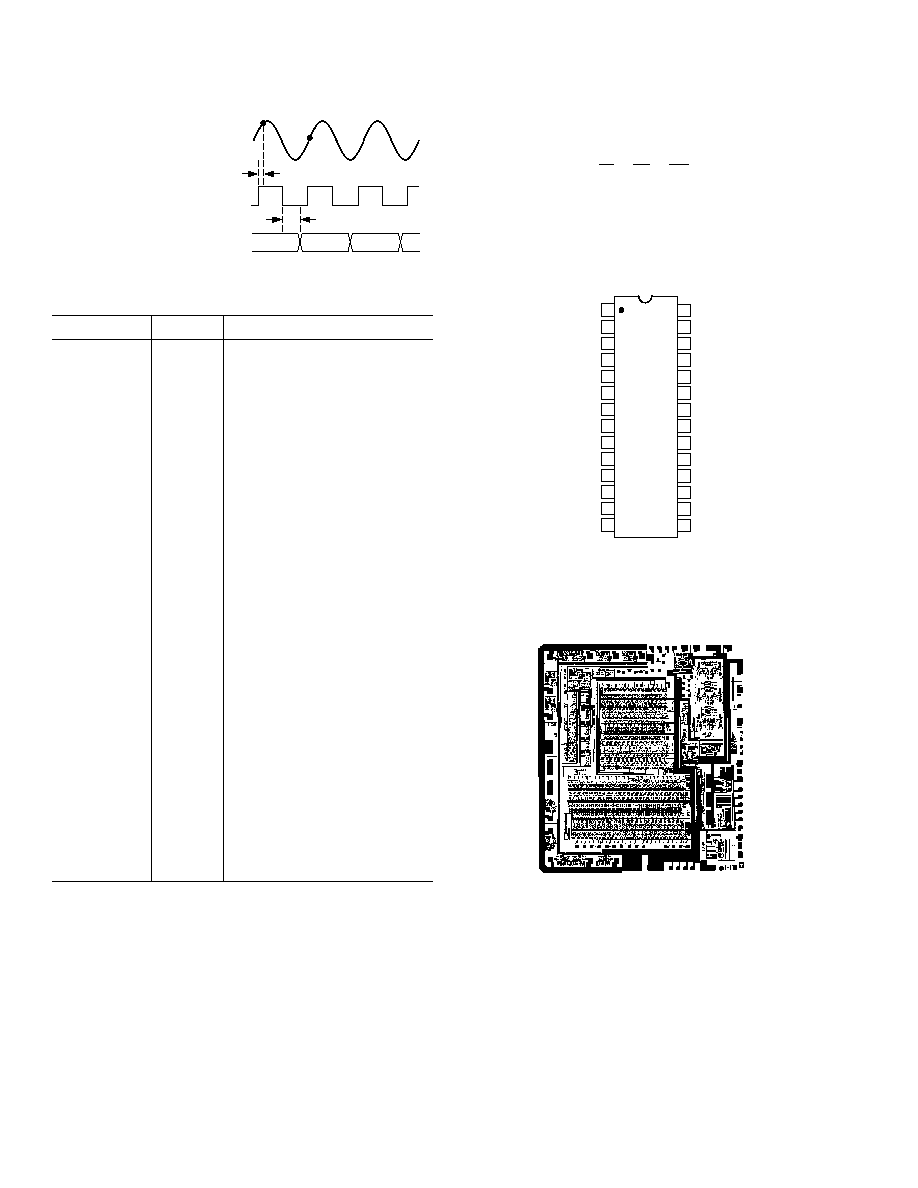
Figure 3. Using Internal Reference
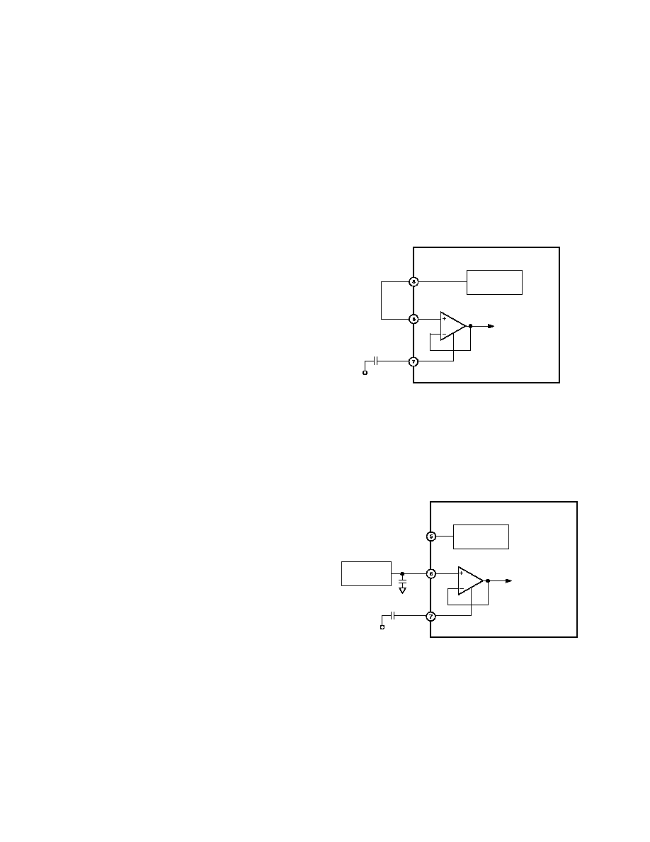
Some applications may require greater accuracy, improved
temperature performance, or adjustment of the gain (input
range) of the AD9040A which cannot be obtained by using the
internal reference. For these applications, an external +2.5 V
reference can be used, as shown in Figure 4. The V
REF
input
requires 5
�
A of drive current.
REF
AMP
BANDGAP
REFERENCE
REFERENCE
AD9040A
0.1 F
V
OUT
V
REF
�V
S
BP
REF
REFERENCE
0.1 F
Figure 4. Using External Reference
AD9040A
REV. B
�7�
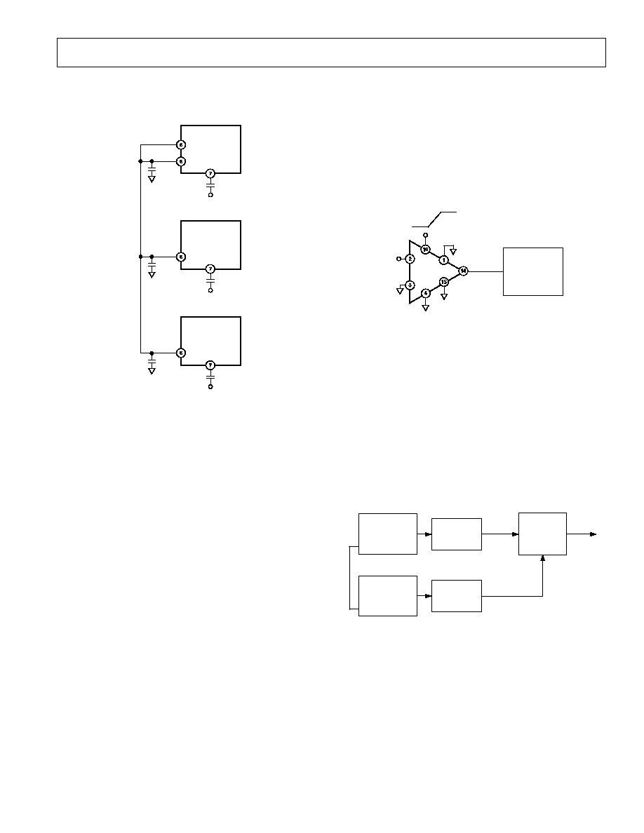
In applications using multiple AD9040As, slaving the reference
inputs to a single reference output will improve gain tracking
among the ADCs, as shown in Figure 5.
V
OUT
V
REF
AD9040A
0.1 F
�V
S
V
REF
AD9040A
V
REF
AD9040A
�V
S
�V
S
0.1 F
0.1 F
0.1 F
0.1 F
0.1 F
Figure 5. Slaving Multiple AD9040As to a Single Internal
Reference
In the specifications table, the Gain Tempco parameter under
DC ACCURACY applies to the ADC when the internal refer-
ence is being used. If an external reference is used, its tempera-
ture coefficient must be taken into account to determine overall
temperature performance.
The input range can be varied by adjusting the reference voltage
applied to the AD9040A. By decreasing the reference voltage,
the gain can be reduced approximately 10% with no degrada-
tion in performance. Increasing the reference voltage increases
the gain; but for proper operation, the reference voltage should
not exceed +2.6 V.
Time-Gain Control ADC
Ultrasound and sonar systems require an increase in gain versus
time. This allows the system to correct for attenuation of return
pulses. Figure 6 shows the AD600/AD602 amplifier and the
AD9040A ADC configured as a time-gain control analog-to-
digital converter. The control voltage ramps from �625 mV to
+625 mV, permitting 40 dB of gain-control range. The voltage
used for gain control can be either a linear ramp, or the output
of a voltage-output DAC such as the AD7242.
AD9040A
A
IN
�625mV
+625mV
GAIN CONTROL
VOLTAGE
AD600/602
Figure 6.
Ultrasound/Sonar Time-Gain Control ADC
Using X-AMPsTM
Transient Response
Figure 7 illustrates the method for evaluating ADC transient
performance. Two synthesizers are locked in synchronization,
but tuned to frequencies which are slightly offset from a 2-to-1
submultiple.
One synthesizer clocks a flat pulse network at a frequency of
19.9609375 MHz to provide the analog input signal; the other
synthesizer output is shaped to provide a CMOS 40 MHz sam-
pling clock. At the output of the AD9040A, output data reflects
an interleaved alias of the input pulse. The repetitive sampling
allows the measurement of ADC transient response as shown in
performance graphs elsewhere in this data sheet.
AD9040A
MARCONI 2030
SYNTHESIZER
REF
MARCONI 2030
SYNTHESIZER
REF
19.9609375 MHz
40 MHz
FLAT PULSE
NETWORK
SINE
TO
CMOS
ANALOG
IN
ENCODE
OUTPUT
Figure 7. Transient Response Test
X-AMP is a trademark of Analog Devices, Inc.

AD9040A
REV. B
�8�
Layout Information
Preserving the accuracy and dynamic performance of the
AD9040A requires that designers pay special attention to the
layout of the printed circuit board.
Analog paths should be kept as short as possible and be properly
terminated to avoid reflections. The analog input and reference
voltage connections should be kept away from digital signal
paths; this reduces the amount of digital switching noise which
is capacitively coupled into the analog section. Digital signal
paths should also be kept short, and run lengths should be
matched to avoid propagation delay mismatch. The AD9040A
digital outputs should be buffered or latched close to the device
(<2 cm). This prevents load transients which may feedback into
the device.
In high speed circuits, layout of the ground is critical. A single,
low impedance ground plane on the component side of the
board is recommended. Power supplies should be capacitively
coupled to the ground plane with high quality chip capacitors to
reduce noise in the circuit. Multilayer boards allow designers to
lay out signal traces without interrupting the ground plane, and
provide low impedance ground planes. In systems with dedi-
cated analog and digital grounds, all grounds of the AD9040A
should be connected to the analog ground plane.
The power supplies of the AD9040A should be isolated from
the supplies used for external devices; this reduces the amount
of noise coupled into the ADC. The digital +5 volt connection
of the device (V
D
, Pin 23) powers the digital outputs and should
be connected to the same supply as +V
S
(Pins 3 and 10). Con-
necting V
D
to a system digital supply may couple noise into the
device. Sockets limit dynamic performance and are not recom-
mended for use with the AD9040A.
EVALUATION BOARD
The evaluation board for the AD9040A (AD9040A/PCB) pro-
vides an easy and flexible method for evaluating the ADC's
performance without (or prior to) developing a user-specific
printed circuit board. The two-sided board includes a recon-
struction DAC and digital output interface, and uses the layout
and applications suggestions outlined above. It is available from
Analog Devices at nominal cost.
Generous space is provided near the analog input and digital
outputs to support additional signal processing components the
user may wish to add. This prototyping area includes through
holes with 100-mil centers to support a variety of component
additions.
Input/Output/Supply Information
Power supply, analog input, clock connections, and recon-
structed output (RC OUTPUT) are identified by labels on the
evaluation board. Operation of the evaluation board should
conform to the following characteristics:
Table I. Evaluation Board Characteristics
Parameter
Typical
Units
Supply Current
+5 V
250
mA
�5.2 V
300
mA
A
IN
Impedance
51
Voltage Range
�
1.0
V
CLOCK
Impedance
51
Frequency
40
MSPS
RC OUTPUT
Impedance
51
Voltage Range
0 V to �1 V
V
Analog Input
Analog input signals can be fed directly into the Device Under
Test input (A
IN
). The A
IN
input is terminated at the device with
a 51
resistor.

AD9040A
REV. B
�9�
Figure 9. PCB Bottom View
Table II. Digital Coding
Analog
Voltage
Out-of-
Input
Level
Range
Digital Output
MSB . . . LSB
+1.002 V
Positive Full Scale + 1 LSB 1
1111111111
+1 V
Positive Full Scale
0
1111111111
Full Scale � 1 LSB
0
1111111110
+1/2 V
Positive 1/2 Scale
0
1100000000
1/2 Scale � 1 LSB
0
1011111111
0 V
Bipolar
Zero
0
10000000000
0
01111111111
�1/2 V
1/2 Scale + 1 LSB
0
0100000000
Negative 1/2 Scale
0
0011111111
�1 V
Full Scale + 1 LSB
0
0000000001
Negative Full Scale
0
0000000000
�1.002 V
Negative Full Scale � 1 LSB 1
0000000000
Figure 8. PCB Top View
DAC Reconstruction
The AD9040A evaluation board provides an onboard AD9721
reconstruction DAC for observing the digitized analog input
signal. The AD9721 is terminated into 51 ohms to provide a
1 V p-p signal at the output (RC OUTPUT).
Output Data
The output data bits are latched with a CMOS 74AC574 which
drives a 40-pin connector (AMP p/n 102153-9). The data and
clock signals are available on the connector per the pin assign-
ments shown on the schematic of the evaluation board. Output
data are available on the falling edge of the clock.

AD9040A
REV. B
�10�
+5V
C7
0.1 F
C8
0.1 F
C9
0.1 F
C10
0.1 F
C11
0.1 F
C12
0.1 F
C18
0.1 F
C14
0.1 F
C15
0.1 F
C16
0.1 F
C17
0.1 F
C13
0.1 F
�5V
�5V
�5V
�5V
+5V
+5V
+5V
GND
GND
GND
GND
GND
U2
AD9040AJR
R2
51
9
10
8
U1
74HC86
D7
R16 100
U3
74AC574
9
8
7
6
5
4
3
2
1
11
12
13
14
15
16
17
18
19
U4
74AC574
2
3
4
5
6
7
8
9
1
11
19
18
17
16
15
14
13
12
CK
OE
1D
2D
3D
4D
5D
6D
7D
8D
1Q
2Q
3Q
4Q
5Q
6Q
7Q
8Q
CK
OE
8D
7D
6D
5D
4D
3D
2D
1D
8Q
7Q
6Q
5Q
4Q
3Q
2Q
1Q
V
REF
V
OUT
NC
A
IN
ENC
�V
S
�V
S
�V
S
+V
S
+V
S
+V
D
GND
GND
GND
GND
GND
BPREF
(MSB)
D9
OR
D8
D7
D6
D5
D4
D3
D2
D1
D0
(LSB)
�5V
E1
D9
D8
D6
D5
D4
D3
D2
D1
D0
R18 100
R17 100
R13 100
R15 100
R14 100
R11 100
R12 100
R9 100
R10 100
U5
AD9721BR
�5V
GND
�5V
GND
�5V
GND
+5V
R7
2k
R5
51
R6
51
C6
0.1 F
C21
10 F
�5V
�5V
RC
OUTPUT
BNC
J5
1
2
3
U1
74HC86
4
5
6
U1
74HC86
U1
74HC86
12
13
11
C1
0.1 F
CLK
+5V
R1
51
AIN
BNC
J1
BNC
J2
CLK
H1
H2
C3
10 F
C2
0.1 F
J7
+5V
C5
10 F
C4
0.1 F
J8
�5V
J9
GND
H3
#4
H4
#4
H5
#4
H6
#4
H40DMC
J3
1
2
3
4
5
6
7
8
9
10
11
12
13
14
15
16
17
18
19
20
CLK
D9
D8
D7
D6
D5
D4
D3
D2
D1
D0
GND
GND
GND
GND
GND
GND
GND
GND
GND
GND
GND
GND
GND
GND
GND
GND
GND
GND
GND
GND
21
22
23
24
25
26
27
28
29
30
31
32
33
34
35
36
37
38
39
40
CAMP IN
�5V
GND
�5V
GND
REF OUT
CAMP OUT
REF IN
IOUT
ANA RET
RSET
�5V
GND
+5V
IOUT
D1 (MSB)
D2
D3
D4
D5
D6
D7
D8
D9
D10 (LSB)
CLOCK
INVERT
Figure 10. PCB Schematic

AD9040A
REV. B
�11�
1.2
0.8
0.6
0.4
1.0
DISSIPATION � Watts
1
2
4
6
10
20
40
60
CLOCK RATE � MSPS
Figure 11. Power Dissipation vs.
Clock Rate
LEAST SIGNIFICANT BITS � LSBs
0
0.5
1.0
40
0
30
20
10
CLOCK RATE � MSPS
Figure 14. Differential Nonlinearity
vs. Clock Rate
60
40
125
55
45
�55
50
85 105
65
45
25
5
�15
�35
SIGNAL-TO-NOISE RATIO � dB
TEMPERATURE � C
ENCODE = 32.2 MSPS
A
IN
= 10.3 MHz
ENCODE = 40.5 MSPS
Figure 17. SNR vs. Temperature
0
2.5
5.0
FREQUENCY � MHz
0
�65
dBc
ENCODE = 40.5 MSPS
f1 IN = 2.25 MHz @ �7 dBFS
f2 IN = 2.35 MHz @ �7 dBFS
2f1 � f2 = �69.4 dBFS
2f2 � f1 = �69.2 dBFS
Figure 20.
60
66
48
42
54
36
28
20
12
4
CLOCK RATE � MSPS
SIGNAL-TO-NOISE RATIO � dB
A = 10.3 MHz
IN
Figure 13. SNR vs. Clock Rate
992
960
928
96
64
32
0
5
10
15
20
25
30
35
40
45
50
0
TIME � ns
AD9040A DIGITAL OUTPUT CODE
1024
Figure 16. Transient Response
(Expanded View)
0
8.0
0
�65
dBc
8.0
FREQUENCY � MHz
16.1
ENCODE = 32.2 MSPS
ANALOG IN = 10.3 MHZ
SNR = 55.37 dB
SNR (w/o har.) = 56.77 dB
2nd HARMONIC = �63.3 dB
3rd HARMONIC = �75.4 dB
Figure 19.
0
�65
0
10.1
20.2
FREQUENCY � MHz
dBc
ENCODE = 40.5 MSPS
ANALOG IN = 10.3 MHz
SNR = 53.38 dB
SNR (w/o har.) = 54.31 dB
2nd HARMONIC = �64.7 dB
3rd HARMONIC = �73.7 dB
Figure 22.
FREQUENCY � MHz
HARMONIC DISTORTION � dBc
�63
�73
�48
�68
�53
�58
1
10
100
2
4
6
20
40 60
SIGNAL-TO-NOISE RATIO � dB
60
42
66
48
54
ENCODE = 40.5 MSPS
HARMONIC
DISTORTION
SNR
Figure 12. Harmonic Distortion
and SNR vs. Analog Input
1024
896
768
640
512
384
256
128
0
5
10
15
20
25
30
35
40
45
50
0
TIME � ns
AD9040A DIGITAL OUTPUT CODE
Figure 15. Transient Response
0
8.0
16.1
FREQUENCY � MHz
0
�65
dBc
ENCODE = 32.2 MSPS
ANALOG IN = 2.3 MHz
SNR = 56.79 dB
SNR (w/o har.) = 57.58 dB
2nd HARMONIC = �68.5 dB
3rd HARMONIC = 80.7 dB
Figure 18.
0
10.1
20.2
FREQUENCY � MHz
0
�65
dBc
ENCODE = 40.5 MSPS
ANALOG IN = 2.3 MHz
SNR = 55.20 dB
SNR (w/o har.) = 55.90 dB
2nd HARMONIC = �75.1 dB
3rd HARMONIC = �73.2 dB
Figure 21.
AD9040A
REV. B
�12�
C1835a�0�5/99
PRINTED IN U.S.A.
OUTLINE DIMENSIONS
Dimensions shown in inches and (mm)
28-Lead Plastic DIP
(N-28)
28
1
14
15
1.565 (39.70)
1.380 (35.10)
0.550 (13.97)
0.530 (13.46)
PIN 1
0.022 (0.558)
0.014 (0.356)
0.015 (0.38)
MIN
0.140
(3.55)
MIN
SEATING
PLANE
0.250
(6.35)
MAX
0.100
(2.54)
BSC
0.070
(1.77)
MAX
0.015 (0.381)
0.008 (0.204)
0.625 (15.87)
0.600 (15.24)
28-Lead SOIC Package
(R-28)
0.012 (0.30)
0.004 (0.10)
0.019 (0.48)
0.014 (0.36)
0.104 (2.64)
0.093 (2.36)
0.050
(1.27)
BSC
0.013 (0.33)
0.009 (0.23)
0.04 (1.02)
0.024 (0.61)
0.712 (18.08)
0.700 (17.78)
0.419 (10.64)
0.393 (9.98)
0.300 (7.60)
0.292 (7.40)
PIN 1
28
15
14
1