 | –≠–ª–µ–∫—Ç—Ä–æ–Ω–Ω—ã–π –∫–æ–º–ø–æ–Ω–µ–Ω—Ç: AD9060JE | –°–∫–∞—á–∞—Ç—å:  PDF PDF  ZIP ZIP |
REV. A
Information furnished by Analog Devices is believed to be accurate and
reliable. However, no responsibility is assumed by Analog Devices for its
use, nor for any infringements of patents or other rights of third parties
which may result from its use. No license is granted by implication or
otherwise under any patent or patent rights of Analog Devices.
a
10-Bit 75 MSPS
A/D Converter
AD9060
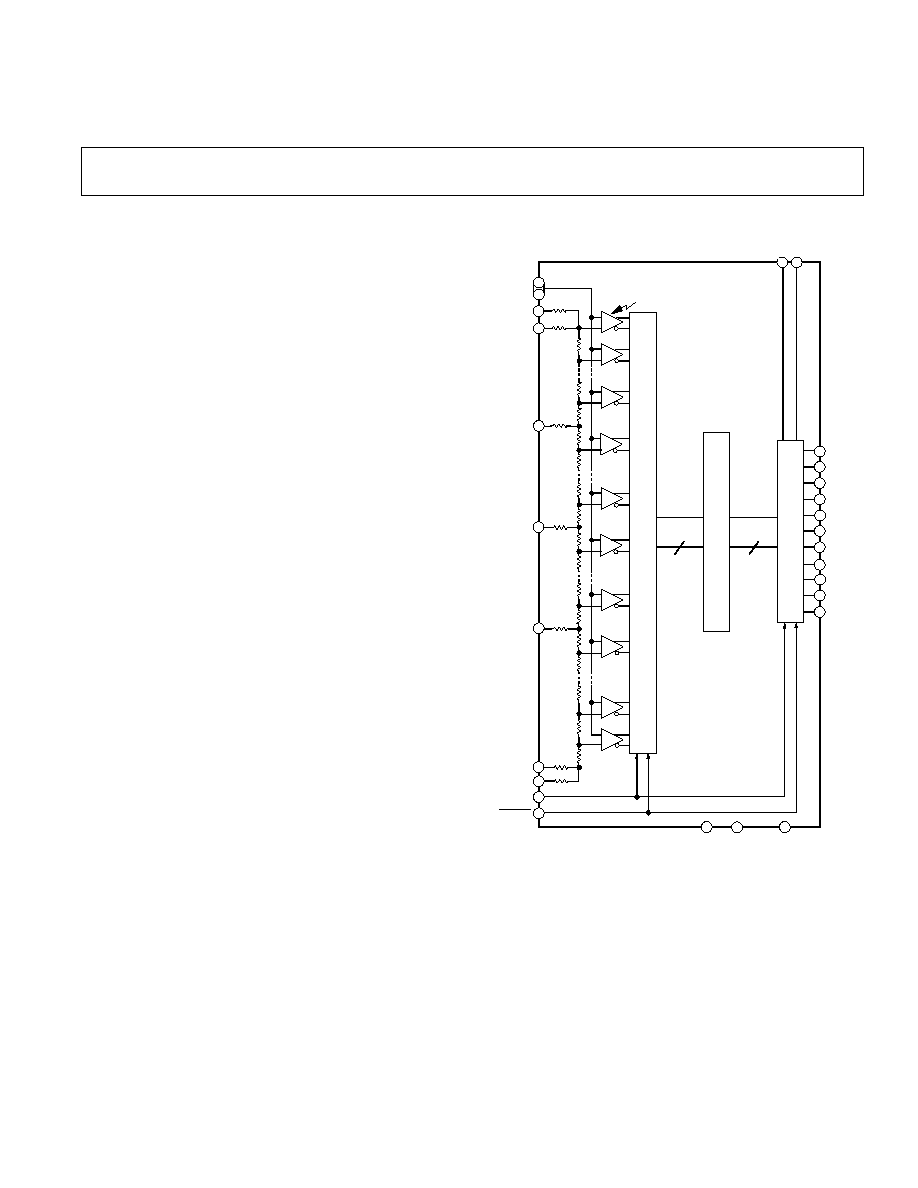
FUNCTIONAL BLOCK DIAGRAM
2
56
1
512
C
O
M
P
A
R
A
T
O
R
L
A
T
C
H
E
S
OVERFLOW
OVERFLOW
1024
10
7
59
61
128
129
256
257
384
385
51
50
49
48
47
46
23
22
21
20
19
OVERFLOW
R
R/2
R
R/2
R
R/2
R
R/2
R
R/2
R
R/2
R
R
11
L
A
T
C
H
63
12
57
14
ENCODE
ANALOG IN
GROUND
OVERFLOW
LSBS
INVERT
MSB
INVERT
R/2
R/2
1
D
E
C
O
D
E
L
O
G
I
C
13
ENCODE
+V
REF
+V
SENSE
≠V
REF
≠V
SENSE
3/4
REF
1/2
REF
1/4
REF
≠V
S
+V
S
D
9
(MSB)
D
8
D
7
D
6
D
5
D
4
D
3
D
2
D
1
D
0
(LSB)
8
9
FEATURES
Monolithic 10-Bit/75 MSPS Converter
ECL Outputs
Bipolar ( 1.75 V) Analog Input
57 dB SNR @ 2.3 MHz Input
Low (45 pF) Input Capacitance
MIL-STD-883 Compliant Versions Available
APPLICATIONS
Digital Oscilloscopes
Medical Imaging
Professional Video
Radar Warning/Guidance Systems
Infrared Systems
GENERAL DESCRIPTION
The AD9060 A/D converter is a 10-bit monolithic converter ca-
pable of word rates of 75 MSPS and above. Innovative architec-
ture using 512 input comparators instead of the traditional 1024
required by other flash converters reduces input capacitance and
improves linearity.
Inputs and outputs are ECL-compatible, which makes the
AD9060 the recommended choice for systems with conversion
rates >30 MSPS to minimize system noise. An overflow bit is
provided to indicate analog input signals greater than +V
SENSE
.
Voltage sense lines are provided to ensure accurate driving of
the
±
V
REF
voltages applied to the units. Quarter-point taps on
the resistor ladder help optimize the integral linearity of the
unit.
Either 68-pin ceramic leaded (gull wing) packages or ceramic
LCCs are available and specifically designed for low thermal im-
pedances. Two performance grades for temperatures of both
0
∞
C to +70
∞
C and ≠55
∞
C to +125
∞
C ranges are offered to allow
the user to select the linearity best suited for each application.
Dynamic performance is fully characterized and production
tested at +25
∞
C. MIL-STD-883 units are available.
The AD9060 A/D converter is available in versions compliant
with MIL-STD-883. Refer to the Analog Devices Military Prod-
ucts Databook or current AD9060/883B data sheet for detailed
specifications.
One Technology Way, P.O. Box 9106, Norwood, MA 02062-9106, U.S.A.
Tel: 617/329-4700
World Wide Web Site: http://www.analog.com
Fax: 617/326-8703
© Analog Devices, Inc., 1997

REV. A
≠2≠
AD9060≠SPECIFICATIONS
ABSOLUTE MAXIMUM RATINGS
1
+V
S
. . . . . . . . . . . . . . . . . . . . . . . . . . . . . . . . . . . . . . . . . +6 V
≠V
S
. . . . . . . . . . . . . . . . . . . . . . . . . . . . . . . . . . . . . . . . . ≠6 V
ANALOG IN . . . . . . . . . . . . . . . . . . . . . . . . . . . . ≠2 V to +2 V
+V
REF
, ≠V
REF
, 3/4
REF
, 1/2
REF
, 1/4
REF
. . . . . . . . . ≠2 V to +2 V
+V
REF
to ≠V
REF
. . . . . . . . . . . . . . . . . . . . . . . . . . . . . . . 4.0 V
ENCODE,
ENCODE . . . . . . . . . . . . . . . . . . . . . . . 0 V to ≠V
S
3/4
REF
, 1/2
REF
, 1/4
REF
Current . . . . . . . . . . . . . . . . . .
±
10 mA
Digital Output Current . . . . . . . . . . . . . . . . . . . . . . . . 20 mA
Operating Temperature
AD9060JE/KE/JZ/KZ . . . . . . . . . . . . . . . . . . 0
∞
C to +70
∞
C
Storage Temperature . . . . . . . . . . . . . . . . . . ≠65
∞
C to +150
∞
C
Maximum Junction Temperature
2
. . . . . . . . . . . . . . . +175
∞
C
Lead Soldering Temp (10 sec) . . . . . . . . . . . . . . . . . . +300
∞
C
ELECTRICAL CHARACTERISTICS
Test
AD9060JE/JZ
AD9060KE/KZ
Parameter (Conditions)
Temp
Level
Min
Typ
Max
Min
Typ
Max
Units
RESOLUTION
10
10
Bits
DC ACCURACY
3
Differential Nonlinearity
+25
∞
C
I
1.0
1.25
0.75
1.0
LSB
Full
VI
1.5
1.25
LSB
Integral Nonlinearity
+25
∞
C
I
1.25
2.0
1.0
1.5
LSB
Full
VI
2.5
2.0
LSB
No Missing Codes
Full
VI
Guaranteed
ANALOG INPUT
Input Bias Current
4
+25
∞
C
I
0.4
1.0
0.4
1.0
mA
Full
VI
2.0
2.0
mA
Input Resistance
+25
∞
C
I
2.0
7.0
2.0
7.0
k
Input Capacitance
4
+25
∞
C
V
45
45
pF
Analog Bandwidth
+25
∞
C
V
175
175
MHz
REFERENCE INPUT
Reference Ladder Resistance
+25
∞
C
I
22
37
56
22
37
56
Full
VI
14
66
14
66
Ladder Tempco
Full
V
0.1
0.1
/
∞
C
Reference Ladder Offset
Top of Ladder
+25
∞
C
I
45
90
45
90
mV
Full
VI
90
90
mV
Bottom of Ladder
+25
∞
C
I
45
90
45
90
mV
Full
VI
90
90
mV
Offset Drift Coefficient
Full
V
50
50
µ
V/
∞
C
SWITCHING PERFORMANCE
Conversion Rate
+25
∞
C
I
75
75
MSPS
Aperture Delay (t
A
)
+25
∞
C
V
1
1
ns
Aperture Uncertainty (Jitter)
+25
∞
C
V
5
5
ps, rms
Output Delay (t
OD
)
5
+25
∞
C
I
2
4
9
2
4
9
ns
Output Rise Time
+25
∞
C
I
1
3
1
3
ns
Output Fall Time
+25
∞
C
I
1
3
1
3
ns
Output Time Slew
5
+25
∞
C
I
1.5
3
1.5
3
ns
DYNAMIC PERFORMANCE
Transient Response
+25
∞
C
V
10
10
ns
Overvoltage Recovery Time
+25
∞
C
V
10
10
ns
Effective Number of Bits (ENOB)
f
IN
= 2.3 MHz
+25
∞
C
I
8.7
9.1
8.7
9.1
Bits
f
IN
= 10.3 MHz
+25
∞
C
IV
8.0
8.6
8.0
8.6
Bits
f
IN
= 29.3 MHz
+25
∞
C
IV
7.0
7.4
7.0
7.4
Bits
Signal-to-Noise Ratio
6
f
IN
= 2.3 MHz
+25
∞
C
I
54
56
54
56
dB
f
IN
= 10.3 MHz
+25
∞
C
I
51
54
51
54
dB
f
IN
= 29.3 MHz
+25
∞
C
I
44
47
44
47
dB
(+V
S
= +5 V; ≠V
S
= ≠5.2 V; V
SENSE
= 1.75 V; ENCODE = 60 MSPS
unless otherwise noted)
3

AD9060
≠3≠
REV. A
Test
AD9060JE/JZ
AD9060KE/KZ
Parameter (Conditions)
Temp
Level
Min
Typ
Max
Min
Typ
Max
Units
DYNAMIC PERFORMANCE
(CONTINUED)
Signal-to-Noise Ratio
6
(Without Harmonics)
f
IN
= 2.3 MHz
+25
∞
C
I
54
56
54
58
dB
f
IN
= 10.3 MHz
+25
∞
C
I
51
55
51
55
dB
f
IN
= 29.3 MHz
+25
∞
C
I
46
48
46
48
dB
Harmonic Distortion
f
IN
= 2.3 MHz
+25
∞
C
I
61
65
61
65
dBc
f
IN
= 10.3 MHz
+25
∞
C
I
55
58
55
58
dBc
f
IN
= 29.3 MHz
+25
∞
C
I
47
50
47
50
dBc
Two-Tone Intermodulation
Distortion Rejection
7
+25
∞
C
V
70
70
dBc
Differential Phase
+25
∞
C
V
0.5
0.5
Degree
Differential Gain
+25
∞
C
V
1
1
%
ENCODE INPUT
Logic "1" Voltage
Full
VI
≠1.1
≠1.1
V
Logic "0" Voltage
Full
VI
≠1.5
≠1.5
V
Logic "1" Current
Full
VI
150
300
150
300
µ
A
Logic "0" Current
Full
VI
150
300
150
300
µ
A
Input Capacitance
+25
∞
C
V
5
5
pF
Pulse Width (High)
+25
∞
C
I
6
6
ns
Pulse Width (Low)
+25
∞
C
I
6
6
ns
DIGITAL OUTPUTS
Logic "1" Voltage
Full
VI
≠1.1
≠1.1
V
Logic "0" Voltage
Full
VI
≠1.5
≠1.5
V
POWER SUPPLY
+V
S
Supply Current
+25
∞
C
VI
420
500
420
500
mA
Full
VI
500
500
mA
≠V
S
Supply Current
+25
∞
C
VI
150
180
150
180
mA
Full
VI
190
190
mA
Power Dissipation
+25
∞
C
VI
2.8
3.3
2.8
3.3
W
Full
VI
3.5
3.5
W
Power Supply Rejection
Ratio (PSRR)
8
Full
VI
6
10
6
10
mV/V
NOTES
1
Absolute maximum ratings are limiting values to be applied individually and beyond which the serviceability of the circuit may be impaired. Functional operability is
not necessarily implied. Exposure to absolute maximum rating conditions for an extended period of time may affect device reliability.
2
Typical thermal impedances (part soldered onto board): 68-pin leaded ceramic chip carrier:
JC
= 1
∞
C/W;
JA
= 17
∞
C/W (no air flow);
JA
= 15
∞
C/W
(air flow = 500 LFM). 68-pin ceramic LCC:
JC
= 2.6
∞
C/W;
JA
= 15
∞
C/W (no air flow);
JA
= 13
∞
C/W (air flow = 500 LFM).
3
3/4
REF
, 1/2
REF
and 1/4
REF
reference ladder taps are driven from dc sources at +0.875 V, 0 V and ≠0.875 V, respectively. Outputs terminated through 100
to ≠2.0 V;
C
L
< 4 pF. Accuracy of the overflow comparator is not tested and not included in linearity specifications.
4
Measured with ANALOG IN = +V
SENSE
5
Output delay measured as worst-case time from 50% point of the rising edge of ENCODE to 50% point of the slowest rising or falling edge of D
0
≠D
9
. Output skew
measured as worst-case difference in output delay among D
0
≠D
9
.
6
RMS signal to rms noise with analog input signal 1 dB below full scale at specified frequency.
7
Intermodulation measured with analog input frequencies of 2.3 MHz and 3.0 MHz at 7 dB below full scale.
8
Measured as the ratio of the worst-case change in transition voltage of a single comparator for a 5% change m +V
S
or ≠V
S
.
Specifications subject to change without notice.
AD9060
≠4≠
REV. A
EXPLANATION OF TEST LEVELS
Test Level
I
≠ 100% production tested.
II ≠ 100% production tested at +25
∞
C and sample tested at
specified temperatures.
III ≠ Sample tested only.
IV ≠ Parameter is guaranteed by design and characterization
testing.
V ≠ Parameter is a typical value only.
VI ≠ All devices are 100% production tested at +25
∞
C. 100%
production tested at temperature extremes for extended
temperature devices; sample tested at temperature extremes
for commercial/industrial devices.
DIE LAYOUT AND MECHANICAL INFORMATION
Die Dimensions . . . . . . . . . . . . . . . . 206
◊
140
◊
15 (
±
2) mils
Pad Dimensions . . . . . . . . . . . . . . . . . . . . . . . . . . . . 4
◊
4 mils
Metalization . . . . . . . . . . . . . . . . . . . . . . . . . . . . . . . . . . . Gold
Backing . . . . . . . . . . . . . . . . . . . . . . . . . . . . . . . . . . . . . None
Substrate Potential . . . . . . . . . . . . . . . . . . . . . . . . . . . . . . . ≠V
S
Passivation . . . . . . . . . . . . . . . . . . . . . . . . . . . . . . . . . . Nitride
WARNING!
ESD SENSITIVE DEVICE
CAUTION
ESD (electrostatic discharge) sensitive device. Electrostatic charges as high as 4000 V readily
accumulate on the human body and test equipment and can discharge without detection.
Although the AD9060 features proprietary ESD protection circuitry, permanent damage may
occur on devices subjected to high energy electrostatic discharges. Therefore, proper ESD
precautions are recommended to avoid performance degradation or loss of functionality.
ORDERING GUIDE
Temperature
Package
Device
Range
Options
1
AD9060JZ
0
∞
C to +70
∞
C
Z-68
AD9060JE
0
∞
C to +70
∞
C
E-68A
AD9060KZ
0
∞
C to +70
∞
C
Z-68
AD9060KE
0
∞
C to +70
∞
C
E-68A
AD9060SZ
2
≠55
∞
C to +125
∞
C
Z-68
AD9060SE
2
≠55
∞
C to +125
∞
C
E-68A
AD9060TZ
2
≠55
∞
C to +125
∞
C
Z-68
AD9060TE
2
≠55
∞
C to +125
∞
C
E-68A
AD9060/PCB
0
∞
C to +70
∞
C
Evaluation Board
NOTES
1
E = Ceramic Leadless Chip Carrier; Z = Ceramic Leaded Chip Carrier.
2
For specifications, refer to Analog Devices Military Products Databook.
AD9060
≠5≠
REV. A
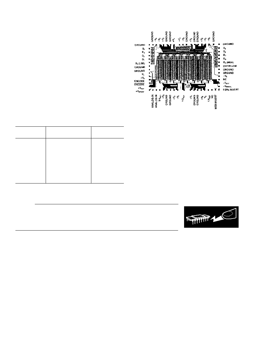
AD9060 PIN DESCRIPTIONS
Pin No.
Name
Function
1
1/2
REF
Midpoint of internal reference ladder.
2, 16, 28, 29, 35,
≠V
S
Negative supply voltage; nominally ≠5.2 V
±
5%.
41, 42, 54, 64
3, 6, 15, 30, 33, 34,
+V
S
Positive supply voltage; nominally +5 V
±
5%.
37, 40, 65, 68
4, 5, 17, 18, 25, 27,
GROUND
All ground pins should be connected together and to low-
31, 32, 36, 38, 39, 43,
impedance ground plane.
45, 52, 53, 66, 67
7
3/4
REF
Three-quarter point of internal reference ladder.
8, 9
ANALOG IN
Analog input; nominally between
±
1.75 V.
11
+V
SENSE
Voltage sense line to most positive point on internal resistor
ladder. Normally +1.75 V.
12
+V
REF
Voltage force connection for top of internal reference ladder.
Normally driven to provide +1.75 V at +V
SENSE
.
13
ENCODE
Differential ECL convert signal that starts digitizing process.
14
ENCODE
ECL-compatible convert command used to begin digitizing process.
19≠23, 46≠50
D
0
≠D
9
ECL-compatible digital output data.
51
OVERFLOW
ECL-compatible output indicating ANALOG IN > +V
SENSE
.
56
≠V
REF
Voltage force connection for bottom of internal reference
ladder. Normally driven to provide ≠1.75 V at ≠V
SENSE
.
57
≠V
SENSE
Voltage sense line to most negative point on internal
resistor ladder. Normally ≠1.75 V.
59
LSBs INVERT
Normally grounded. When connected to +V
S
, lower order
bits (D
0
≠D
8
) are inverted. Not ECL-compatible.
61
MSB INVERT
Normally grounded. When connected to +V
S
, most
significant bit (MSB; D
9
) is inverted. Not ECL-compatible.
63
1/4
REF
One-quarter point of internal reference ladder.
60
9
10
61
44
43
27
26
AD9060
TOP VIEW
(Not to scale)
NC
ENCODE
GND
(LSB) D
0
D
4
NC
NC
ANALOG IN
ANALOG IN
GND
GND
1/4
REF
NC
GND
GND
MSB INVERT
NC
LSBs INVERT
NC
GND
OVERFLOW
D
9
(MSB)
NC
GND
GND
GND
GND
GND
GND
GND
ENCODE
GND
GND
GND
GND
NC
D
2
D
1
D
3
D
6
D
8
D
5
D
7
1/2
REF
3/4
REF
+V
SENSE
≠V
SENSE
+V
REF
≠V
REF
≠V
S
+V
S
+V
S
≠V
S
+V
S
+V
S
+V
S
≠V
S
≠V
S
+V
S
≠V
S
≠V
S
+V
S
+V
S
≠V
S
+V
S
+V
S
≠V
S
≠V
S
AD9060 Pin Designations
AD9060
≠6≠
REV. A
MIL-STD-883 Compliance Information
The AD9060 devices are classified within Microcircuits Group
57, Technology Group D (bipolar A/D converters) and are con-
structed in accordance with MIL-STD-883. The AD9060 is
electrostatic sensitive and falls within electrostatic sensitivity
classification Class 1. Percent Defective Allowance (PDA) is
computed based on Subgroup 1 of the specified Group A test
list. Quality Assurance (QA) screening is in accordance with Al-
ternate Method A of Method 5005.
The following apply: Burn-In per 1015; Life Test per 1005;
Electrical Testing per 5004. (Note: Group A electrical testing
assumes T
A
= T
C
= T
J
.) MIL-STD-883-compliant devices are
marked with "C" to indicate compliance.
AD9060
4,5,17,
18,25,27,
31,32,36,
38,39,43,
45,52,53,66,67
100
ANALOG IN
ENCODE
GROUND
2,16,28,29,35,
41,42,54,64
0.1
µ
F
0.1
µ
F
AD1
AD2
3,6,15,30,33,34,
37,40,55,65,68
LSB INVERT
STATIC:
DYNAMIC:
AD1 = ≠2V; AD 2 = ECL HIGH
AD3 = ECL LOW
AD1 =
±
2V TRIANGLE WAVE
AD2,AD3 = ECL PULSE TRAIN
9
46
19
14
51
12
8
56
59
61
+2V
≠2V
+V
REF
≠V
REF
D
5
≠ D
9
D
0
≠ D
4
+V
S
5.0V
+
13
ENCODE
AD3
≠5.2V
MSB
INVERT
23
510
510
510
≠V
S
510
510
AD9060 Burn-ln Connections
THEORY OF OPERATION
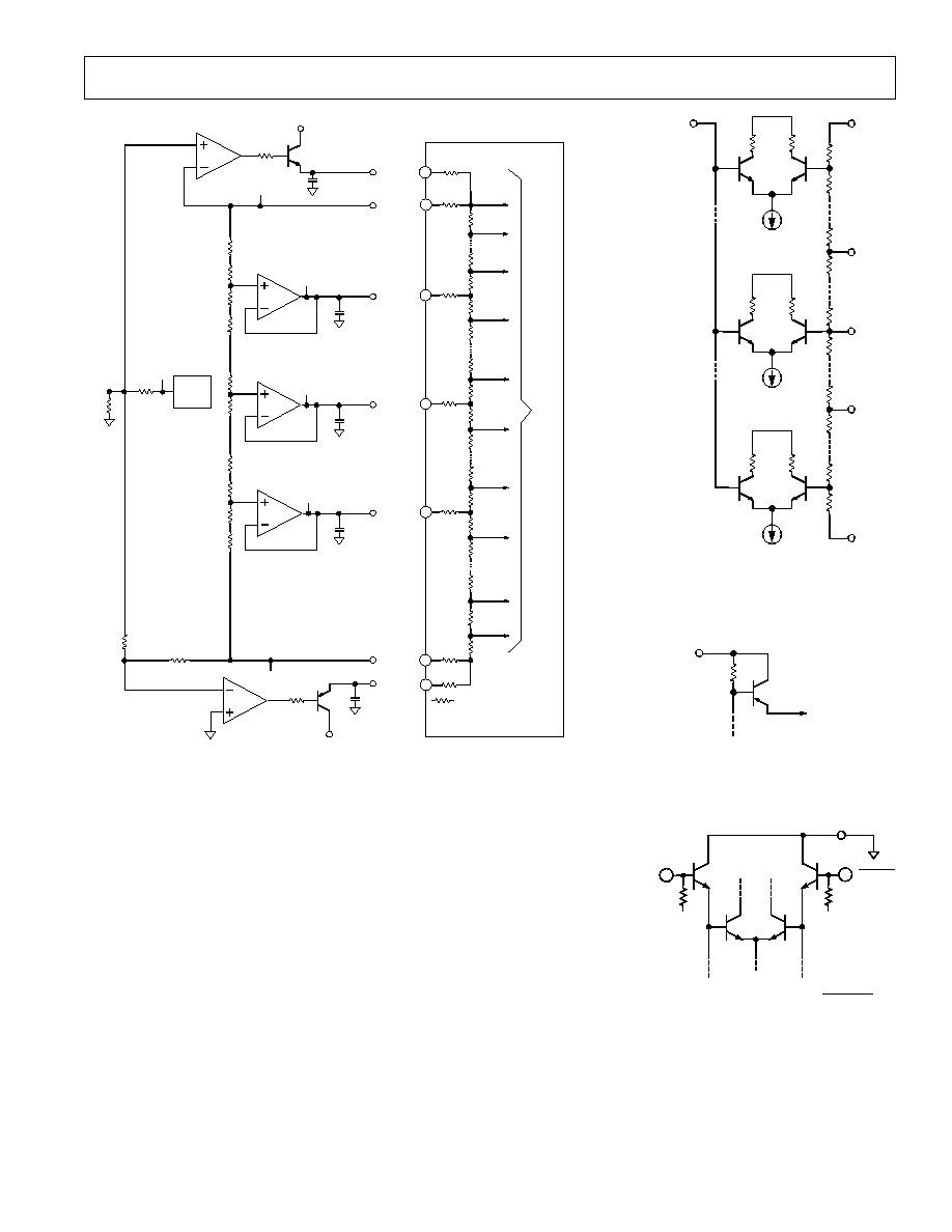
Refer to the AD9060 block diagram. As shown, the AD9060
uses a modified "flash," or parallel, A/D architecture. The ana-
log input range is determined by an external voltage reference
(+V
REF
and ≠V
REF
), nominally
±
1.75 V. An internal resistor
ladder divides this reference into 512 steps, each representing
two quantization levels. Taps along the resistor ladder (1/4
REF
,
1/2
REF
and 3/4
REF
) are provided to optimize linearity. Rated
performance is achieved by driving these points at 1/4, 1/2 and
3/4, respectively, of the voltage reference range.
The A/D conversion for the nine most significant bits (MSBs) is
performed by 512 comparators. The value of the least signifi-
cant bit (LSB) is determined by a unique interpolation scheme
between adjacent comparators. The decoding logic processes
the comparator outputs and provides a 10-bit code to the out-
put stage of the converter.
Flash architecture has an advantage over other A/D architec-
tures because conversion occurs in one step. This means the
performance of the converter is limited primarily by the speed
and matching of the individual comparators. In the AD9060, an
innovative interpolation scheme takes advantage of flash archi-
tecture but minimizes the input capacitance, power and device
count usually associated with that method of conversion.
These advantages occur because of using only half the normal
number of input comparator cells to accomplish the conversion.
In addition, a proprietary decoding scheme minimizes error
codes. Input control pins allow the user to select from among
Binary, Inverted Binary, Twos Complement and Inverted Twos
Complement coding (see AD9060 Truth Table).
APPLICATIONS
Many of the specifications used to describe analog/digital con-
verters have evolved from system performance requirements in
these applications. Different systems emphasize particular speci-
fications, depending on how the part is used. The following ap-
plications highlight some of the specifications and features that
make the AD9060 attractive in these systems.
Wideband Receivers
Radar and communication receivers (baseband and direct IF
digitization), ultrasound medical imaging, signal intelligence and
spectral analysis all place stringent ac performance requirements
on analog-to-digital converters (ADCs). Frequency domain
characterization of the AD9060 provides signal-to-noise ratio
(SNR) and harmonic distortion data to simplify selection of the
ADC.
Receiver sensitivity is limited by the Signal-to-Noise Ratio (SNR)
of the system. The SNR for an ADC is measured in the fre-
quency domain and calculated with a Fast Fourier Transform
(FFT). The SNR equals the ratio of the fundamental compo-
nent of the signal (rms amplitude) to the rms value of the
"noise." The noise is the sum of all other spectral components,
including harmonic distortion but excluding dc.
Good receiver design minimizes the level of spurious signals in
the system. Spurious signals developed in the ADC are the result
of imperfections in the device transfer function (nonlinearities,
delay mismatch, varying input impedance, etc.). In the ADC,
these spurious signals appear as Harmonic Distortion. Harmonic
Distortion is also measured with an FFT and is specified as the
ratio of the fundamental component of the signal (rms ampli-
tude) to the rms value of the worst case harmonic (usually the
2nd or 3rd).

AD9060
≠7≠
REV. A
Two-Tone Intermodulation Distortion (IMD) is a frequently cited
specification in receiver design. In narrow-band receivers, third-
order IMD products result in spurious signals in the pass band
of the receiver. Like mixers and amplifiers, the ADC is charac-
terized with two, equal amplitude, pure input frequencies. The
IMD equals the ratio of the power of either of the two input sig-
nals to the power of the strongest third order IMD signal. Un-
like mixers and amplifiers, the IMD does not always behave as it
does in linear devices (reduced input levels do not result in pre-
dictable reductions in IMD).
Performance graphs provide typical harmonic and SNR data for
the AD9060 for increasing analog input frequencies. In choosing
an A/D converter, always look at the dynamic range for the ana-
log input frequency of interest. The AD9060 specifications pro-
vide guaranteed minimum limits at three analog test frequencies.
Aperture Delay is the delay between the rising edge of the EN-
CODE command and the instant at which the analog input is
sampled. Many systems require simultaneous sampling of more
than one analog input signal with multiple ADCs. In these situ-
ations timing is critical, and the absolute value of the aperture
delay is not as critical as the matching between devices.
Aperture Uncertainty, or jitter, is the sample-to-sample variation
in aperture delay. This is especially important when sampling
high slew rate signals in wide bandwidth systems. Aperture un-
certainty is one of the factors that degrades dynamic perfor-
mance as the analog input frequency is increased.
Digitizing Oscilloscopes
Oscilloscopes provide amplitude information about an observed
waveform with respect to time. Digitizing oscilloscopes must ac-
curately sample this signal without distorting the information to
be displayed.
One figure of merit for the ADC in these applications is Effective
Number of Bits (ENOBs). ENOB is calculated with a sine wave
curve fit and equals:
ENOB = N ≠ LOG
2
[Error (measured)/Error (ideal)]
N is the resolution (number of bits) of the ADC. The measured
error is the actual rms error calculated from the converter out-
puts with a pure sine wave input.
The Analog Bandwidth of the converter is the analog input fre-
quency at which the spectral power of the fundamental signal is
reduced 3 dB from its low frequency value. The analog band-
width is a good indicator of a converter's slewing capabilities.
The Maximum Conversion Rate is defined as the encode rate at
which the SNR for the lowest analog signal test frequency tested
drops by no more than 3 dB below the guaranteed limit.
Imaging
Visible and infrared imaging systems each require similar char-
acteristics from ADCs. The signal input (from a CCD camera
or multiplexer) is a time division multiplexed signal consisting
of a series of pulses whose amplitude varies in direct proportion
to the intensity of the radiation detected at the sensor. These
varying levels are then digitized by applying encode commands
at the correct times, as shown below.
ENCODE
A
IN
AD9060
+F
S
≠F
S
Imaging Application Using AD9060
The actual resolution of the converter is limited by the thermal
and quantization noise of the ADC. The low frequency test for
SNR or ENOB is a good measure of the noise of the AD9060.
At this frequency, the static errors in the ADC determine the
useful dynamic range of the ADC.
Although the signal being sampled does not have a significant
slew rate, this does not imply dynamic performance is not im-
portant. The Transient Response and Overvoltage Recovery Time
specifications ensure that the ADC can track full-scale changes
in the analog input sufficiently fast to capture a valid sample.
Transient Response is the time required for the AD9060 to
achieve full accuracy when a step function is applied. Overvolt-
age Recovery Time is the time required for the AD9060 to re-
cover to full accuracy after an analog input signal 150% of full
scale is reduced to the full-scale range of the converter.
Professional Video
Digital Signal Processing (DSP) is now common in television
production. Modern studios rely on digitized video to create
state-of-the-art special effects. Video instrumentation also re-
quires high resolution ADCs for studio quality measurement
and frame storage.
The AD9060 provides sufficient resolution for these demanding
applications. Conversion speed, dynamic performance and ana-
log bandwidth are suitable for digitizing both composite and
RGB video sources.
AD9060
≠8≠
REV. A
The select resistors (R
S
) shown in the schematic (each pair can
be a potentiometer) are chosen to adjust the quarter-point
voltage references but are not necessary if R1≠R4 match
within 0.05%.
EFFECTIVE NUMBER OF BITS (ENOB)
SIGNAL-TO-NOISE (SNR) ≠ dB
32
38
44
50
56
62
10.0
9.0
8.0
7.0
6.0
5.0
0.4
0.8
1.0
1.4
1.8
2.0
±V
SENSE
≠ Volts
0.6
1.2
1.6
AD9060 SNR and ENOB vs. Reference Voltage
An alternative approach for defining the quarter-point references
of the resistor ladder to evaluate the integral linearity error of an
individual device and adjust the voltage at the quarter-points to
minimize this error. This may improve the low frequency ac
performance of the converter.
Performance of the AD9060 has been optimized with an analog
input voltage of
±
1.75 V (as measured at
±
V
SENSE
). If the ana-
log input range is reduced below these values, relatively larger
differential nonlinearity errors may result because of comparator
mismatches. As shown in the figure below, performance of the
converter is a function of
±
V
SENSE
.
Applying a voltage greater than 4 V across the internal resistor
ladder will cause current densities to exceed rated values and
may cause permanent damage to the AD9060. The design of
the reference circuit should limit the voltage available to the
references.
Analog Input Signal
The signal applied to ANALOG IN drives the inputs of 512
parallel comparator cells (see Equivalent Analog Input figure).
This connection has a typical input resistance of 7 k
and input
capacitance of 45 pF. The input capacitance is nearly constant
over the analog input voltage range as shown in the graph, which
illustrates that characteristic.
The analog input signal should be driven from a low distortion,
low noise amplifier. A good choice is the AD9617, a wide band-
width, monolithic operational amplifier with excellent ac and dc
performance. The input capacitance should be isolated by a
small series resistor (24
for the AD9617) to improve the ac
performance of the amplifier (see AD9060/PCB Evaluation
Board Block Diagram).
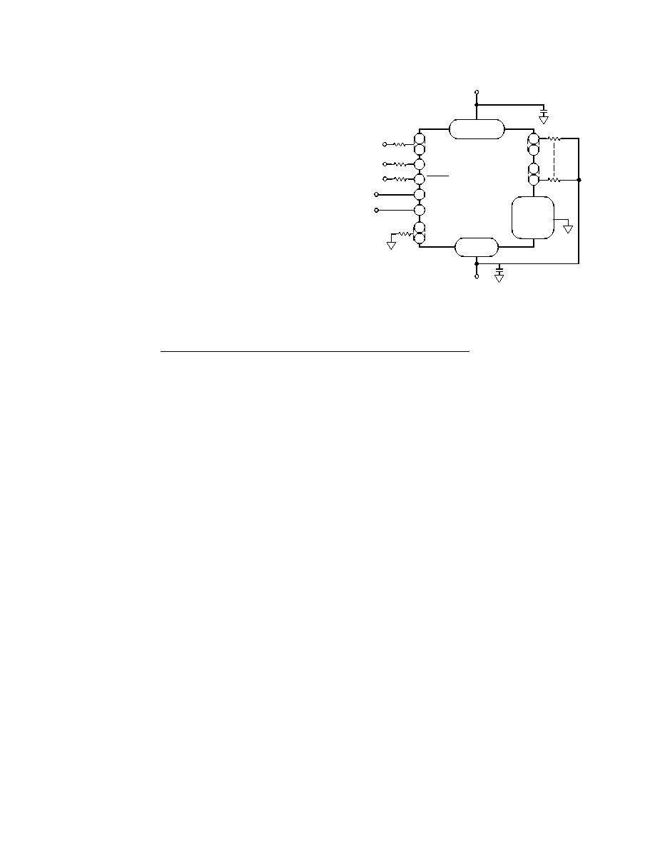
USING THE AD9060
Voltage References
The AD9060 requires the user to provide two voltage references:
+V
REF
and ≠V
REF
. These two voltages are applied across an inter-
nal resistor ladder (nominally 37
) and set the analog input
voltage range of the converter. The voltage references should be
driven from a stable, low impedance source. In addition to these
two references, three evenly spaced taps on the resistor ladder
(1/4
REF
, 1/2
REF
, 3/4
REF
) are available. Providing a reference to
these quarter points on the resistor ladder will improve the inte-
gral linearity of the converter and improve ac performance. (AC
and dc specifications are tested while driving the quarter points
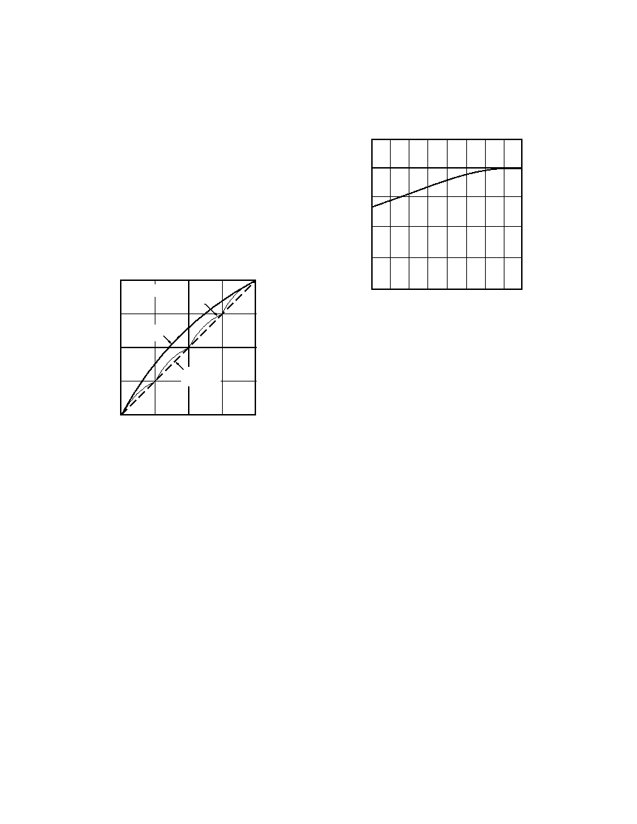
at the indicated levels.) The figure below is not intended to show
the transfer characteristic of the ADC but illustrates how the lin-
earity of the device is affected by reference voltages applied to
the ladder.
0000000000
0100000000
1000000000
1100000000
1111111111
OUTPUT CODE
V
IN
≠V
SENSE
+V
SENSE
3/4
REF
1/2
REF
1/4
REF
TAPS
FLOATING
IDEAL
LINEARITY
TAPS
DRIVEN
(NOT TO SCALE)
Effect of Reference Taps on Linearity
Resistance between the reference connections and the taps of the
first and last comparators causes offset errors. These errors,
called "top and bottom of the ladder offsets," can be nulled by
using the voltage sense lines, +V
SENSE
and ≠V
SENSE
, to adjust the
reference voltages. Current through the sense lines should be
limited to less than 100
µ
A. Excessive current drawn through the
voltage sense lines will affect the accuracy of the sense line
voltage.
The next page shows a reference circuit that nulls out the offset
errors using two op amps, and provides appropriate voltage refer-
ences to the quarter-point taps. Feedback from the sense lines
causes the op amps to compensate for the offset errors. The two
transistors limit the amount of current drawn directly from the
op amps; resistors at the base connections stabilize their opera-
tion. The 10 k
resistors (R1≠R4) between the voltage sense
lines form an external resistor ladder; the quarter point voltages
are taken off this external ladder and buffered by an op amp. The
actual values of resistors R1≠R4 are not critical, but they should
match well and be large enough (
10 k
) to limit the amount of
current drawn from the voltage sense lines.
AD9060
≠9≠
REV. A
≠0.875V
= WIRING
TO COMPARATORS
≠1.75V
0.1
µ
F
R3
R4
0.1
µ
F
AD580
0V
10k
R1
R
S
0.1
µ
F
R2
0.1
µ
F
150
AD9060
+V
REF
56
R
R/2
R
R/2
R
R/2
R
R/2
R
R/2
R
R/2
R
R
11
12
57
≠V
SENSE
+V
SENSE
R/2
R/2
*
*
63
7
3/4
REF
1/4
REF
1/2
REF
1/2
AD708
1/2
AD708
1/2
AD708
1/2
AD708
0.1
µ
F
+5V
+1.75V
1
*
RESISTANCE = < 5
+0.875V
≠5V
+2.5V
+1.75V
R
S
R
S
R
S
10k
10k
150
356
20k
20k
1/2
AD708
150
10k
≠V
REF
AD9060 Reference Circuit
ANALOG INPUT
3/4
REF
1/2
REF
1/4
REF
+V
SENSE
≠V
SENSE
AD9060 Equivalent Analog Input
DIGITAL BITS
AND OVERFLOW
GROUND
AD9060 Equivalent Digital Outputs
GROUND
14
≠V
S
13
ENCODE
ENCODE
≠V
S
AD9060 Encode and Encode
Equivalent Circuits
AD9060
≠10≠
REV. A
DATA FOR N
DATA FOR N + 1
DATA
OUTPUT
N
N + 1
N
N + 1
ANALOG
INPUT
ENCODE
t
OD
t
a
t
a
≠ Aperture Delay
t
OD
≠ Output Delay
ENCODE
AD9060 Timing Diagram
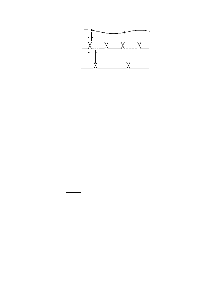
Timing
In the AD9060, the rising edge of the ENCODE signal triggers
the A/D conversion by latching the comparators. (See the
AD9060 Timing Diagram.) These ENCODE and
ENCODE
signals are ECL compatible and should be driven differentially.
Jitter on the ENCODE signal will raise the noise floor of the
converter. Differential signals, with fast clean edges, will reduce
the jitter in the signal and allow optimum ac performance. In
applications with a fixed, high frequency encode rate, converter
performance is also improved (jitter reduced) by using a crystal
oscillator as the system clock.
The AD9060 units are designed to operate with a 50% duty
cycle encode signal; adjustment of the duty cycle may improve
the dynamic performance of individual devices. Since the EN-
CODE and
ENCODE signals are differential, the logic levels are
not critical. Users should remember, however, that reduced logic
levels will reduce the slew rate of the edges and effectively in-
crease the jitter of the signal. ECL terminations for the EN-
CODE and
ENCODE signals should be as close as possible to
the AD9060 package to avoid reflections.
In systems where only single-ended signals are available, the use
of a high speed comparator (such as the AD96685) is recom-
mended to convert to differential signals. An alternative is to
connect +1.3 V (ECL midpoint) to
ENCODE and drive the
ENCODE connection single ended. In such applications, clean,
fast edges are necessary to minimize jitter in the signal.
Output data of the AD9060, D
0
≠D
9
and OVERFLOW are also
ECL compatible and should be terminated through 100
to
≠2 V (or an equivalent load).
Data Format
The format of the output data (D
0
≠D
9
) is controlled by the MSB
INVERT and LSBs INVERT pins. These inputs are dc control
inputs and should be connected to GROUND or +V
S
. The
AD9060 Truth Table gives information to choose from among
Binary, Inverted Binary, Twos Complement and Inverted Twos
Complement coding.
The OVERFLOW output is an indication that the analog input
signal has exceeded the voltage at +V
SENSE
. The accuracy of the
overflow transition voltage and output delay are not tested or in-
cluded in the data sheet limits. Performance of the overflow in-
dicator is dependent on circuit layout and slew rate of the en-
code signal. The operation of this function does not affect the
other data bits (D
0
≠D
9
). It is not recommended for applications
requiring a critical measure of analog input voltage.
Layout and Power Supplies
Proper layout of high speed circuits is always critical but is par-
ticularly important when both analog and digital signals are
involved.
Analog signal paths should be kept as short as possible and be
properly terminated to avoid reflections. The analog input volt-
age and the voltage references should be kept away from digital
signal paths; this reduces the amount of digital switching noise
that is capacitively coupled into the analog section of the circuit.
Digital signal paths should also be kept short, and run lengths
should be matched to avoid propagation delay mismatch. Ter-
minations for ECL signals should be as close as possible to the
receiving gate.
In high speed circuits, layout of the ground circuit is a critical
factor. A single, low impedance ground plane on the component
side of the board will reduce noise on the circuit ground. Power
supplies should be capacitively coupled to the ground plane to
reduce noise in the circuit. Multilayer boards allow designers to
lay out signal traces, without interrupting the ground plane, and
provide low impedance power planes.
It is especially important to maintain the continuity of the
ground plane under and around the AD9060. In systems with
dedicated digital and analog grounds, all grounds of the
AD9060 should be connected to the analog ground plane.
The power supplies (+V
S
and ≠V
S
) of the AD9060 should be
isolated from the supplies used for external devices; this further
reduces the amount of noise coupled into the A/D converter.
Sockets limit the dynamic performance and should be used only
for prototypes or evaluation--PCK Elastomerics Part No. CCS6855
is recommended for the LCC package. (Tel. 215-672-0787)
An evaluation board is available to aid designers and provide a
suggested layout.
AD9060
≠11≠
REV. A
1
2
4
6
8 10
20
60
100
200
40
EF
F
E
CT
I
VE NUM
BER O
F
BI
T
S
(
E
NO
B)
INPUT FREQUENCY ≠ MHz
SI
G
NAL
-
T
O
-
NOI
SE (
S
NR)
≠
d
B
20
26
32
38
44
50
56
62
10.0
9.0
8.0
7.0
6.0
5.0
4.0
ENCODE RATE = 60MSPS
+25∞C
≠55∞C & +125∞C
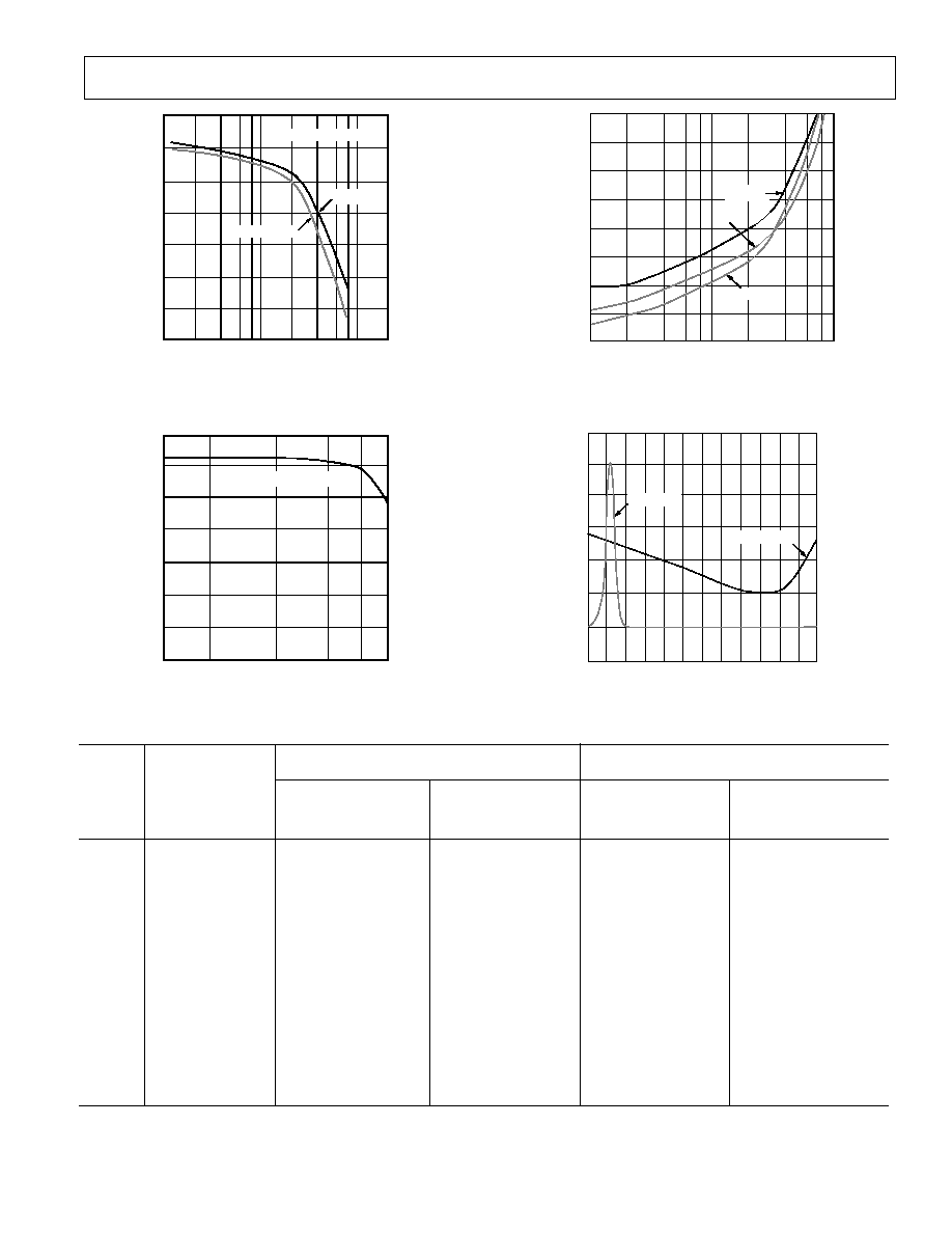
AD9060 SNR and ENOB vs. Input Frequency
EFFECTIVE NUMBER OF BITS (ENOB)
SIGNAL-TO-NOISE (SNR) ≠ dB
20
26
32
38
44
50
56
62
10.0
9.0
8.0
7.0
6.0
5.0
4.0
10
20
40
100
CONVERSION RATE ≠ MSPS
60
ANALOG INPUT = 2.3MHz
80
AD9060 SNR and ENOB vs. Conversion Rate
1
2
4
6
8 10
20
60
100
40
HARMONICS ≠ dBc
40
45
50
55
60
65
70
INPUT FREQUENCY ≠ MHz
35
30
+125
∞
C
≠55
∞
C
+25
∞
C
AD9060 Harmonics vs. Input Frequency
INPUT CAPACITANCE ≠ pF
ANALOG INPUT (A
IN
) ≠ Volts
48
47
45
44
≠1.8
≠1.2
≠0.6
0
10
70
60
50
40
30
20
INPUT RESISTANCE ≠ k
+0.6
+1.2
+1.8
46
RESISTANCE
CAPACITANCE
Input Capacitance/Resistance vs. Input Voltage
Offset Binary
Twos Complement
Step
Range
True
Inverted
True
Inverted
0 = ≠1.75 V
MSB INV = "0"
MSB INV = "1"
MSB INV = "1"
MSB INV = "0"
FS = +1.75 V
LSBs INV = "0"
LSBs INV = "1"
LSBs INV = "0"
LSBs INV = "1"
1024
> + 1.7500
(1)1111111111
(l)0000000000
(1)0111111111
(1)1000000000
1023
+ 1.7466
1111111111
0000000000
0111111111
1000000000
1022
+ 1.7432
1111111110
0000000001
0111111110
1000000001
.
.
.
.
.
.
.
.
.
.
.
.
.
.
.
.
.
.
512
+0.0034
1000000000
0111111111
0000000000
1111111111
511
0.000
0111111111
1000000000
1111111111
0000000000
510
≠0.0034
0111111110
1000000001
1111111110
0000000001
.
.
.
.
.
.
.
.
.
.
.
.
.
.
.
.
.
.
02
≠ 1.7432
0000000010
1111111101
1000000010
0111111101
01
≠ 1.7466
0000000001
1111111110
1000000001
0111111110
00
< ≠ 1.7466
0000000000
1111111111
1000000000
0111111111
The overflow bit is always 0 except where noted in parentheses ( ). MSB INVERT and LSBs INVERT are considered dc controls.
AD9060 Truth Table
AD9060
≠12≠
REV. A
C1349b≠1≠5/97
PRINTED IN U.S.A.
REFERENCE
CIRCUIT
AD9060
DUT
ANALOG
INPUT
50
DUT
ANALOG
INPUT
J2
400
BUFFERED
ANALOG
INPUT
TO ERROR
WAVEFORM
CIRCUIT
OUTPUT
DATA
CONNECTOR
ECL
LATCHES
ENCODE
TIMING
CIRCUIT
CLK
Q
DATA
READY
DAC
OUT
TO ERROR
WAVEFORM
CIRCUIT
AD9617
U5
+V
S
≠V
S
AD9712 DAC
I
OUT
D
+V
REF
+V
SENSE
3/4
REF
MSB INVERT
≠5V
+5V
LSBs INVERT
(LSB) D
0
D
1
(MSB) D
9
OVERFLOW
D
D
D
D
D
D
D
D
D
D
D
GND
DIFFERENTIAL
ECL CLOCK
ENCODE
200
24
50
+5V
D
2
D
3
D
4
D
5
D
6
D
7
D
8
1/2
REF
1/4
REF
≠V
REF
≠V
SENSE
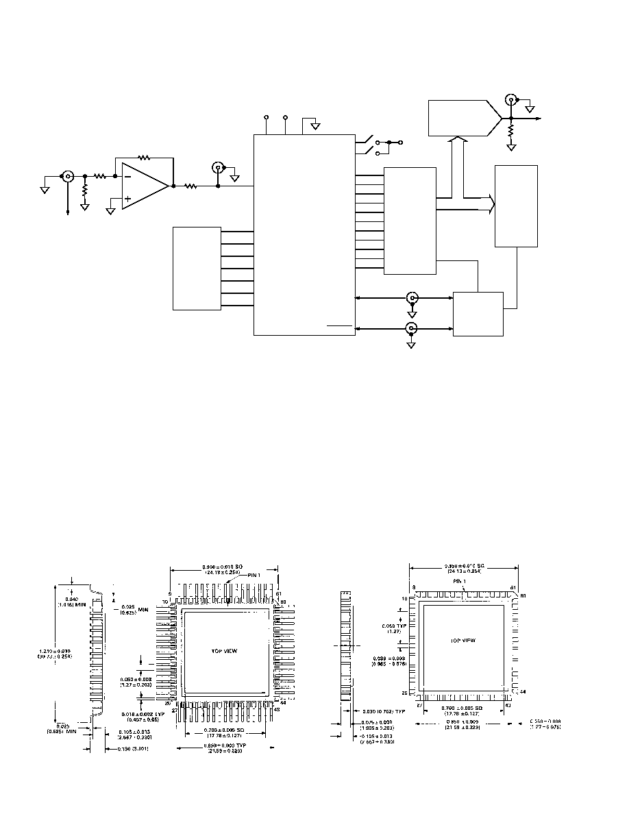
AD9060/PCB Evaluation Board Block Diagram
Onboard reconstruction of the digital data is provided through
the AD9712, a 12-bit monolithic DAC. The analog and recon-
structed waveforms can be summed on the board to allow the
user to observe the linearity of the AD9060 and the effects of the
quarter-point voltages. The digital data and an adjustable Data
Ready signal are available via a 37-pin edge connector.
AD9060/PCB EVALUATION BOARD
The AD9060/PCB Evaluation Board is available from the fac-
tory and is shown here in block diagram form. The board in-
cludes a reference circuit that allows the user to adjust both
references and the quarter-point voltages. The AD9617 is in-
cluded as the drive amplifier, and the user can configure the
gain from ≠1 to ≠15.
Leaded Ceramic Chip Carrier
Suffix Z
Leadless Chip Carrier (LCC)
Suffix E
OUTLINE DIMENSIONS
Dimensions shown in inches and (mm).