 | –≠–ª–µ–∫—Ç—Ä–æ–Ω–Ω—ã–π –∫–æ–º–ø–æ–Ω–µ–Ω—Ç: AD9101 | –°–∫–∞—á–∞—Ç—å:  PDF PDF  ZIP ZIP |

REV. 0
Information furnished by Analog Devices is believed to be accurate and
reliable. However, no responsibility is assumed by Analog Devices for its
use, nor for any infringements of patents or other rights of third parties
which may result from its use. No license is granted by implication or
otherwise under any patent or patent rights of Analog Devices.
a
125 MSPS Monolithic
Sampling Amplifier
One Technology Way, P.O. Box 9106, Norwood, MA 02062-9106, U.S.A.
Tel: 617/329-4700
Fax: 617/326-8703
FUNCTIONAL BLOCK DIAGRAM
CLOCK
CLOCK
V
IN
C
HOLD
4X
AMP
+
RTN
R
3R
≠
+
SAMPLER
≠
AD9101
V
OUT
FEATURES
350 MHz Sampling Bandwidth
125 MHz Sampling Rate
Excellent Hold Mode Distortion
≠75 dB @ 50 MSPS (25 MHz V
IN
)
≠57 dB @ 125 MSPS (50 MHz V
IN
)
7 ns Acquisition Time to 0.1%
<1 ps Aperture Jitter
66 dB Feedthrough Rejection @ 50 MHz
3.3 nV/
Hz Spectral Noise Density
APPLICATIONS
Direct IF Sampling
Digital Sampling Oscilloscopes
HDTV Cameras
Peak Detectors
Radar/EW/ECM
Spectrum Analysis
Test Equipment/CCD Testers
DDS DAC Deglitcher
GENERAL DESCRIPTION
The AD9101 is an extremely accurate, general purpose, high
speed sampling amplifier. Its fast and accurate acquisition speed
allows for a wide range of frequency vs. resolution performance.
The AD9101 is capable of 8 to 12 bits of accuracy at clock rates
of 125 MSPS or 50 MSPS, respectively. This level of perfor-
mance makes it an ideal driver for almost all 8- to 12-bit A/D
encoders on the market today.
In effect, the AD9101 is a track-and-hold with a post amplifier.
This configuration allows the front end sampler to operate at
relatively low signal amplitudes. This results in dramatic im-
provement in both track and hold mode distortion while keeping
power low.
The gain-of-four output amplifier has been optimized for fast
and accurate large signal step settling characteristics even when
heavily loaded. This amplifier's fast Settling Time Linearity
(STL) characteristic causes the amplifier to be transparent to
the low signal level distortion of the sampler. When sampled,
output distortion levels reflect only the distortion performance
of the sampler.
Dramatic SNR and distortion improvements can be realized
when using the AD9101 with high speed flash converters. Flash
converters generally have excellent linearity at dc and low fre-
quencies. However, as signal slew rate increases, their perfor-
mance degrades due to the internal comparators' aperture delay
variations and finite gain bandwidth product.
The benefits of using a track-and-hold ahead of a flash converter
have been well known for many years. However, before the
AD9101, there was no track-and-hold amplifier with sufficient
bandwidth and linearity to markedly increase the dynamic per-
formance of such flashes as the AD9002, AD9012, AD9020,
and AD9060.
A new application made possible by the AD9101 is direct IF-
to-digital conversion. Utilizing the Nyquist principle, the IF
frequency can be rejected, and the baseband signal can be
recovered. As an example, a 40 MHz IF is modulated by a
10 MHz bandwidth signal. By sampling at 25 MSPS, the signal
of interest is detected.
The AD9101 is offered in commercial and military temperature
ranges. Commercial versions include the AD9101AR in plastic
SOIC and AD9101AE in ceramic LCC. Military devices are
available in ceramic LCC. Contact the factory for availability of
versions in DIP and/or military versions.
PRODUCT HIGHLIGHTS
1. Guaranteed Hold-Mode Distortion
2. 125 MHz Sampling Rate to 8 Bits; 50 MHz to 12 Bits
3. 350 MHz Sampling Bandwidth
4. Super-Nyquist Sampling Capability
5. Output Offset Adjustable
AD9101

REV. 0
≠2≠
AD9101≠SPECIFICATIONS
ELECTRICAL CHARACTERISTICS
(+V
S
= +5 V, ≠V
S
= ≠5.2 V, R
LOAD
= 100
, R
lN
= 50
unless otherwise noted)
Test
AD9101
Parameter
Conditions
Temp
Level
Min
Typ
Max
Units
DC ACCURACY
Gain
V
IN
= 0.5 V
25
∞
C
I
3.93
4
4.07
V/V
V
IN
= 0.5 V
Full
VI
3.9
4.1
V/V
Offset
V
IN
= 0 V
25
∞
C
I
±
3
±
10
mV
V
IN
= 0 V
Full
VI
±
15
mV
Output Resistance
25
∞
C
V
0.4
Output Drive Capability
Full
VI
±
60
±
70
mA
PSRR
V
S
= 0.5 V p-p
25
∞
C
VI
37
43
dB
Pedestal Sensitivity to Positive Supply
V
S
= 0.5 V p-p
Full
V
4
mV/V
Pedestal Sensitivity to Negative Supply
V
S
= 0.5 V p-p
Full
V
8
mV/V
ANALOG INPUT/OUTPUT
Output Voltage Range
Full
VI
±
2.4
±
2.7
V
Input Bias Current
25
∞
C
I
±
5
±
15
µ
A
Full
VI
±
20
µ
A
Input Capacitance
25
∞
C
V
2
pF
Input Resistance
25
∞
C≠T
MAX
VI
30
125
k
T
MIN
VI
25
k
CLOCK/CLOCK INPUTS
Input Bias Current
CL/CL = ≠1.0 V
Full
VI
3
3.6
mA
Input Low Voltage (V
IL
)
1
V
IN
= 0.5 V p-p
Full
VI
≠1.8
≠1.5
V
Input High Voltage (V
IH
)
1
V
IN
= 0.5 V p-p
Full
VI
≠1.0
≠0.8
V
TRACK MODE DYNAMICS
Bandwidth (≠3 dB)
V
OUT
= 1 V p-p
Full
IV
160
250
MHz
Slew Rate
4 Volt Output Step
Full
IV
1300
1800
V/
µ
s
Overdrive Recovery Time
2
(to 0.1%)
V
IN
=
±
1 V to 0 V
25
∞
C
V
55
ns
Integrated Output Noise
(5 MHz≠200 MHz) 25
∞
C
V
210
µ
V
Input RMS Spectral Noise @ 10 MHz
25
∞
C
V
3.3
µ
V/
Hz
HOLD MODE DYNAMICS
Worst Harmonic (23 MHz, 50 MSPS)
V
OUT
= 2 V p-p
25
∞
C
V
≠75
dBFS
Worst Harmonic (48 MHz, 100 MSPS)
V
OUT
= 2 V p-p
25
∞
C
IV
≠62
≠57
dBFS
Worst Harmonic (48 MHz, 100 MSPS)
V
OUT
= 2 V p-p
Full (Ind.)
IV
≠53
dBFS
Worst Harmonic (48 MHz, 100 MSPS)
V
OUT
= 2 V p-p
Full (Mil.)
IV
≠51
dBFS
Worst Harmonic (48 MHz, 125 MSPS)
V
OUT
= 2 V p-p
25
∞
C
V
≠57
dBFS
Sampling Bandwidth (≠3 dB)
3
V
IN
= 0.5 V p-p
25
∞
C
V
350
MHz
Hold Noise
4
(RMS)
Full
V
150
◊
t
H
mV/s
Droop Rate
25
∞
C
I
±
5
±
18
mV/
µ
s
Full
VI
±
40
mV/
µ
s
Feedthrough Rejection (50 MHz)
V
OUT
= 2 V p-p
Full
V
≠66
dB
TRACK-TO-HOLD SWITCHING
Aperture Delay
25
∞
C
V
≠250
ps
Aperture Jitter
25
∞
C
V
<1
ps rms
Pedestal Offset
V
IN
= 0 V
25
∞
C
I
±
5
±
20
mV
V
IN
= 0 V
Full
VI
±
35
mV
Transient Amplitude
V
IN
= 0 V
Full
V
8
mV
Settling Time to 4 mV
V
IN
= 0 V
Full
V
4
ns
Glitch Product
5
V
IN
= 0 V
25
∞
C
V
20
pV-s
HOLD-TO-TRACK SWITCHING
Acquisition Time to 0.1%
2 V Output Step
25
∞
C
V
7
ns
Acquisition Time to 0.01%
2 V Output Step
25
∞
C
IV
11
14
ns
2 V Output Step
Full
IV
16
ns
POWER SUPPLY
+V
S
Current
Full
VI
55
70
mA
≠V
S
Current
Full
VI
59
73
mA
Power Dissipation
Full
VI
570
715
mW

NOTES
1
If the analog input exceeds
±
300 mV, the clock levels should be shifted as shown in the Theory of Operation section entitled "Driving the Encode Clock."
2
Time to recover within rated error band from 160% overdrive.
3
Sampling bandwidth is defined as the ≠3 dB frequency response of the input sampler to the hold capacitor when operating in the sampling mode. It is greater than
tracking bandwidth because it does not include the bandwidth of the output amplifier.
4
Hold mode noise is proportional to the length of time a signal is held. For example, if the hold time (t
H
) is 20 ns, the accumulated noise is typically 3
µ
V
(150 mV/s
◊
20 ns). This value must be combined with the track mode noise to obtain total noise.
5
Total energy of worst case track-to-hold or hold-to-track glitch.
Specifications subject to change without notice.
≠3≠
REV. 0
AD9101
20-Pin SOIC
RTN
RTN
C
B+
CLK
NC
V
IN
V
OUT
GND
CLK
GND
GND
1
2
3
4
5
6
7
8
9
10
20
19
18
17
16
15
14
13
12
11
TOP VIEW
(Not to Scale)
AD9101
+V
S
+V
S
+V
S
+V
S
C
B≠
≠V
S
≠V
S
≠V
S
≠V
S
20-Contact Ceramic LCC
1
2
3
4
5
6
7
8
9
10
11
12
13
14
15
16
17
18
19 20
BOTTOM VIEW
RTN
RTN
GND
GND
C
B≠
CLK
≠V
S
NC
V
IN
V
OUT
GND
CLK
C
B+
≠V
S
+V
S
+V
S
+V
S
≠V
S
≠V
S
+V
S
PIN CONFIGURATIONS
ABSOLUTE MAXIMUM RATINGS
1
Supply Voltage (+V
S
) . . . . . . . . . . . . . . . . . . . . ≠0.5 V to +6 V
Supply Voltage (≠V
S
) . . . . . . . . . . . . . . . . . . . . ≠6 V to +0.5 V
Analog Input Voltage . . . . . . . . . . . . . . . . . . . . . . . . . . . .
±
5 V
CLOCK/CLOCK Input . . . . . . . . . . . . . . . . . ≠5 V to +0.5 V
Continuous Output Current
4
. . . . . . . . . . . . . . . . . . . . 70 mA
Storage Temperature . . . . . . . . . . . . . . . . . . ≠65
∞
C to +150
∞
C
Operating Temperature Range
AE, AR . . . . . . . . . . . . . . . . . . . . . . . . . . . . ≠40
∞
C to +85
∞
C
SE . . . . . . . . . . . . . . . . . . . . . . . . . . . . . . ≠55
∞
C to +125
∞
C
Junction Temperature (Ceramic)
2
. . . . . . . . . . . . . . . +175
∞
C
Junction Temperature (Plastic)
2
. . . . . . . . . . . . . . . . +150
∞
C
Soldering Temperature (1 minute)
3
. . . . . . . . . . . . . . +220
∞
C
NOTES
1
Absolute maximum ratings are limiting values to be applied individually, and
beyond which the serviceability of the circuit may be impaired. Functional
operability is not necessarily implied. Exposure to absolute maximum rating
conditions for an extended period of time may affect device reliability.
2
Typical thermal impedances (no air flow, soldered to PC board) are as follows:
Ceramic LCC:
JA
= 48
∞
C/W;
JC
= 9.9
∞
C/W; Plastic SOIC:
JA
= 54
∞
C/W;
JC
= 7.3
∞
C/W.
3
For surface mount devices, mounted by vapor phase soldering. Prior to vapor phase
soldering, plastic units should receive a minimum eight hour bakeout at 110
∞
C to
drive off any moisture absorbed in plastic during shipping or storage. Through-hole
devices can be soldered at +300
∞
C for 10 seconds.
4
Output is short circuit protected to ground. Continuous short circuit may affect
device reliability.
Pin Description
Pin
Description
Connection
1
RTN
Gain Set Resistor Return*
2
RTN
Gain Set Resistor Return*
3
C
B+
Bootstrap Capacitor (Positive Bias)
4
+V
S
+5 V Power Supply (Analog)
5
+V
S
+5 V Power Supply (Analog)
6
GND
Hold Capacitor Ground
7
GND
Hold Capacitor Ground
8
+V
S
+5 V Power Supply (Digital)
9
+V
S
+5 V Power Supply (Digital)
10
CLK
True ECL T/H Clock
11
CLK
Complement ECL T/H Clock
12
≠V
S
≠5.2 V Power Supply (Digital)
13
≠V
S
≠5.2 V Power Supply (Digital)
14
N/C
No Connection
15
V
IN
Analog Signal Input
16
GND
Ground (Signal Return)
17
≠V
S
≠5.2 V Power Supply (Analog)
18
≠V
S
≠5.2 V Power Supply (Analog)
19
C
B≠
Bootstrap Capacitor (Negative Bias)
20
V
OUT
Analog Signal Output
*See "Matching the AD9101 to A/D Encoders." Both pins should either be
grounded or connected to voltage source for offset.
WARNING!
ESD SENSITIVE DEVICE
CAUTION
ESD (electrostatic discharge) sensitive device. Electrostatic charges as high as 4000 V readily
accumulate on the human body and test equipment and can discharge without detection.
Although the AD9101 features proprietary ESD protection circuitry, permanent damage may
occur on devices subjected to high energy electrostatic discharges. Therefore, proper ESD
precautions are recommended to avoid performance degradation or loss of functionality.
EXPLANATION OF TEST LEVELS
Test Level
I
≠ 100% production tested.
II ≠ 100% production tested at +25
∞
C, and sample tested at
specified temperatures.
III ≠ Periodically sample tested.
IV ≠ Parameter is guaranteed by design and characterization
testing.
V
≠ Parameter is a typical value only.
VI ≠ All devices are 100% production tested at +25
∞
C. 100%
production tested at temperature extremes for extended
temperature devices; sample tested at temperature
extremes for commercial/industrial devices.
ORDERING INFORMATION
Temperature
Package
Package
Model
Range
Description
Option
AD9101AR
≠40
∞
C to +85
∞
C
Plastic SOIC
R-20
AD9101AE
≠40
∞
C to +85
∞
C
LCC
E-20A
AD9101SE
≠55
∞
C to +125
∞
C
LCC
E-20A

AD9101
≠4≠
REV. 0
Acquisition Time is the amount of time it takes the AD9101
to reacquire the analog input when switching from hold to track
mode. The interval starts at the 50% clock transition point and
ends when the input signal is reacquired to within a specified
error band at the hold capacitor.
Aperture Delay establishes when the input signal is actually
sampled. It is the time difference between the analog propaga-
tion delay of the front-end buffer and the control switch delay
time (the time from the hold command transition to when the
switch is opened). For the AD9101, this is a negative value,
meaning that the analog delay is longer than the switch delay.
Aperture Jitter is the random variation in the aperture delay.
This is measured in ps-rms and is manifested as phase noise on
the held signal.
Droop Rate is the change in output voltage as a function of
time (dV/dt). It is measured at the AD9101 output with the de-
vice in hold mode and the input held at a specified dc value; the
measurement starts immediately after the T/H switches from
track to hold.
Feedthrough Rejection is the ratio of the output signal to the
input signal when in hold mode. This is a measure of how well
the switch isolates the input signal from feeding through to the
output.
Hold-to-Track Switch Delay is the time delay from the track
command to the point when the output starts to change to ac-
quire a new signal level.
Pedestal Offset is the offset voltage measured immediately af-
ter the AD9101 is switched from track to hold with the input
held at zero volts. It manifests itself as a dc offset during the
hold time.
Sampling Bandwidth is the ≠3 dB frequency response from
the input to the hold capacitor under sampling conditions. It is
greater than the tracking bandwidth because it does not include
the bandwidth of the output amplifier which is optimized for
settling time rather than bandwidth.
Track-to-Hold Settling Time is the time necessary for the
track to hold switching transient to settle to within 4 mV of its
final value.
Track-to-Hold Switching Transient is the maximum peak
switch induced transient voltage which appears at the AD9101
output when it is switched from track to hold.
CLOCK
INPUTS
+2V
0V
-2V
ANALOG
INPUT (x 4)
+2V
0V
-2V
"1"
"0"
HOLD TO TRACK
SWITCH DELAY
TIME (1.5 ns)
APERTURE
DELAY
(≠0.25 ns)
"TRACK"
ACQUISITION
TIME (SEE
TEXT)
VOLTAGE
LEVEL HELD
"HOLD"
SAMPLER OUTPUT SIGNAL (x 4)
AND AMPLIFIER OUTPUT SIGNAL
OBSERVED AT
HOLD CAPACITOR
OBSERVED AT
AMPLIFIER OUTPUT
"HOLD"
CLOCK
CLOCK
CLOCK
TRACK TO
HOLD
SETTLING
(4 ns)
Timing Diagram (500 ps/div)
AD9101
≠5≠
REV. 0
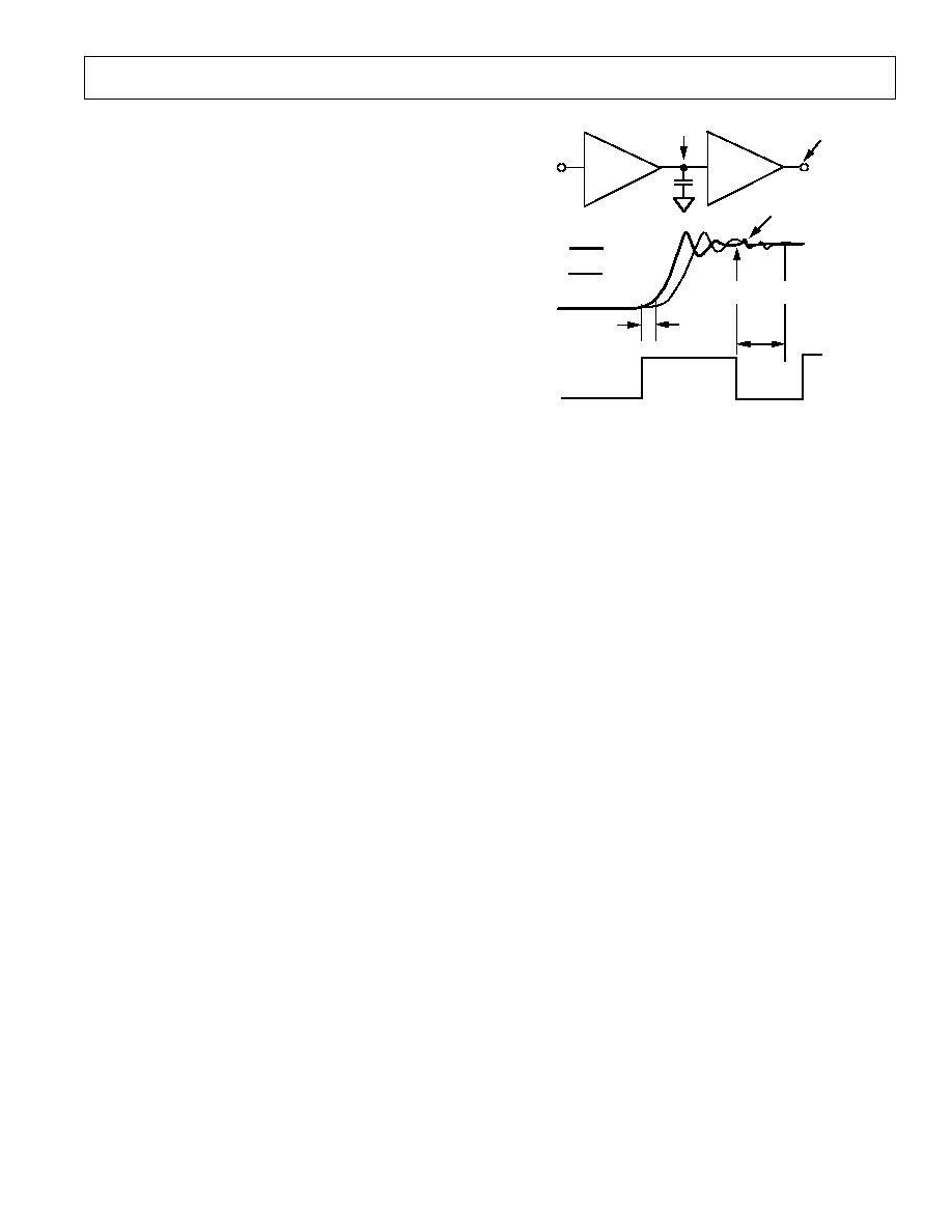
V
OUT
TS
ACQUISITION TIME
AT HC TO X%
V
OUT
TRACK
HOLD
TRACK-TO-HOLD
INDUCED GLITCH
V
HC
t
DHT
1.5ns
V
HC
AMP
HC
SAMPLER
Figure 1. Acquisition Time at Hold Capacitor
during the track time. However, since the output amplifier al-
ways "tracks" the front end circuitry, it "catches up" and di-
rectly superimposes itself (less about 500 ps of analog delay) to
V
HC
. Since the small signal settling time of the output amplifier
can be about 1.2 ns to
±
1 mV, and is significantly less than the
hold time, acquisition time should be referenced to the hold
capacitor.
Most of the hold settling time and output acquisition time are
due to the sampler and the switch network. (Output acquisition
time is as seen on a scope at the output. This is typically 1.7 ns
longer than actual acquisition time.) For track time, the output
amplifier contributes only about 5 ns of the total; in hold mode,
it contributes 1.7 ns (as stated above).
A stricter definition of acquisition would actually include both
the acquisition and track-to-hold settling times to a defined ac-
curacy. To obtain 12-bit+ distortion levels and 50 MSPS opera-
tion, the minimum recommended track and hold times are
12 ns and 8 ns, respectively. To drive an 8-bit flash converter
(such as the AD9002) with a 2 V p-p full-scale input, hold time
to 1 LSB accuracy will be limited primarily by the aperture time
of the encoder, rather than by the AD9101. This makes it pos-
sible to reduce track time to as little as 5 ns, with hold time cho-
sen to optimize the encoder's performance.
Though acquisition time and track-to-hold settling time to
1/2 LSB (0.4%) accuracy are 6 ns and 4 ns respectively, it is still
possible to achieve ≠45 dB SNR performance at clock speeds to
125 MSPS. This is because the settling error is roughly propor-
tional to the signal level and is partially cancelled due to the
high phase margin of the input sampler.
Hold vs. Track Mode Distortion
In many traditional high speed, open-loop track-and-holds,
track mode distortion is often much better than hold mode dis-
tortion. Track mode distortion does not include nonlinearities
due to the switch network, and does not correlate to the relevant
hold mode distortion. But since hold mode distortion has tradi-
tionally been omitted from manufacturer's specification tables,
users have had to discover for themselves the effective overall
hold mode distortion of the combined T/H and encoder.
THEORY OF OPERATION
The AD9101 employs a new and unique track-and-hold archi-
tecture. Previous commercially available high speed track-and-
holds used an open loop input buffer, followed by a diode
bridge, hold capacitor, and output buffer (closed or open loop)
with a FET device usually connected to the hold capacitor. This
architecture required mixed device technology and, usually, hy-
brid construction. The sampling rate of these hybrids has been
limited to 20 MSPS for 12-bit accuracy. Distortion generated in
the front-end amplifier/bridge limited the dynamic range perfor-
mance to the "mid ≠70 dBFS" for analog input signals of less
than 10 MHz. Broadband and switch-generated noise limited
the SNR of previous track-and-holds to about 70 dB.
The AD9101 is a monolithic device using a high frequency
complementary bipolar process to achieve new levels of high
speed precision. Its architecture completely breaks from the tra-
ditional architecture described above. The hold switch has been
integrated into the first stage closed-loop buffer. This innova-
tion provides error (distortion) correction for both the switch
and buffer while still achieving slew rates representative of an
open-loop design. In addition, acquisition slew current for the
hold capacitor is higher than the traditional diode bridge switch
configurations, removing a main contributor to the limits of
maximum sampling rate, input frequency, and distortion.
The closed-loop output amplifier includes zero voltage bias cur-
rent cancellation, which results in high-temperature droop rates
close to those found in FET type inputs. This closed-loop am-
plifier inherently provides high speed loop correction and has
extremely low distortion even when heavily loaded.
Extremely fast time constant linearity (7 ns to 0.01% for a 4 V
output step) ensures that the output amplifier does not limit the
AD9101 sampling rate or analog input frequency. (The acquisi-
tion and settling time are primarily limited only by the input
sampler.) The output is transparent to the overall AD9101 hold
mode distortion levels for loads as low as 50
.
Full-scale track and acquisition slew rates achieved by the
AD9101 are 1800 V/
µ
s and 1700 V/
µ
s, respectively. When com-
bined with excellent phase margin (typically 5% overshoot),
wide bandwidth, and dc gain accuracy, acquisition time to
0.01% is only 11 ns.
Acquisition Time
Acquisition time is the amount of time it takes the AD9101 to
reacquire the analog input when switching from hold-to-track
mode. The interval starts at the 50% clock transition point and
ends when the input signal is reacquired to within a specified er-
ror band at the hold capacitor.
The hold-to-track switch delay (t
DHT
) cannot be subtracted
from this acquisition time for 12-bit performance because it is a
charging time and analog output delay that occurs when moving
from hold to track; this delay is typically 1.5 ns. Therefore, the
track time required for the AD9101 is the acquisition time
which includes t
DHT
. Note that the acquisition time is defined as
the settled voltage at the hold capacitor and does not include the
delay and settling time of the output amplifier. The example in
Figure 1 illustrates why the output amplifier does not contribute
to the overall acquisition time.
The exaggerated illustration in Figure 1 shows that V
HC
has
settled to within x% of its final value, but V
OUT
(due to slew rate
limitations, finite BW, power supply ringing, etc.) has not settled