 | ÐлекÑÑоннÑй компоненÑ: AD9214 | СкаÑаÑÑ:  PDF PDF  ZIP ZIP |
Äîêóìåíòàöèÿ è îïèñàíèÿ www.docs.chipfind.ru
REV. D
Information furnished by Analog Devices is believed to be accurate and
reliable. However, no responsibility is assumed by Analog Devices for its
use, nor for any infringements of patents or other rights of third parties that
may result from its use. No license is granted by implication or otherwise
under any patent or patent rights of Analog Devices.
a
AD9214
One Technology Way, P.O. Box 9106, Norwood, MA 02062-9106, U.S.A.
Tel: 781/329-4700
www.analog.com
Fax: 781/326-8703
© Analog Devices, Inc., 2002
10-Bit, 65/80/105 MSPS
3 V A/D Converter
FUNCTIONAL BLOCK DIAGRAM
REF
TIMING
10
10
AGND
AD9214
AV
DD
DrV
DD
PWRDWN
OR
D
9
D
0
DGND
ENCODE
A
IN
A
IN
DFS/GAIN
REFSENSE
REF
PIPELINE
ADC
CORE
T/H
BUFFER
OUTPUT REGISTER
FEATURES
SNR = 57 dB @ 39 MHz Analog Input (0.5 dBFS)
Low Power
190 mW at 65 MSPS
285 mW at 105 MSPS
30 mW Power-Down Mode
300 MHz Analog Bandwidth
On-Chip Reference and Track/Hold
1 V p-p or 2 V p-p Analog Input Range Option
Single 3.3 V Supply Operation (2.7 V3.6 V)
Two's Complement or Offset Binary Data Format Option
APPLICATIONS
Battery-Powered Instruments
Hand-Held Scopemeters
Low-Cost Digital Oscilloscopes
Ultrasound Equipment
Cable Reverse Path
Broadband Wireless
Residential Power Line Networks
PRODUCT DESCRIPTION
The AD9214 is a 10-bit monolithic sampling analog-to-digital
converter (ADC) with an on-chip track-and-hold circuit, and
is optimized for low cost, low power, small size, and ease of use.
The product operates up to 105 MSPS conversion rate with
outstanding dynamic performance over its full operating range.
The ADC requires only a single 3.3 V (2.7 V to 3.6 V) power
supply and an encode clock for full performance operation. No
external reference or driver components are required for many
applications. The digital outputs are TTL/CMOS compatible
and a separate output power supply pin supports interfacing
with 3.3 V or 2.5 V logic.
The clock input is TTL/CMOS compatible. In the power-down
state, the power is reduced to 30 mW. A gain option allows
support for either 1 V p-p or 2 V p-p analog signal input swing.
Fabricated on an advanced CMOS process, the AD9214 is
available in a 28-lead surface-mount plastic package (28-SSOP)
specified over the industrial temperature range (40
°C to +85°C).
PRODUCT HIGHLIGHTS
High Performance--Outstanding ac performance from 65 MSPS
to 105 MSPS. SNR greater than 55 dB typical and as high
as 58 dB.
Low Power--The AD9214 at 285 mW consumes a fraction of
the power available in existing high-speed monolithic solutions.
In sleep mode, power is reduced to 30 mW.
Single Supply--The AD9214 uses a single 3 V supply, simplify-
ing system power supply design. It also features a separate digital
output driver supply line to accommodate 2.5 V logic families.
Small Package--The AD9214 is packaged in a small 28-lead
surface-mount plastic package (28-SSOP).

REV. D
2
AD9214SPECIFICATIONS
DC SPECIFICATIONS
Test
AD9214-65
AD9214-80
AD9214-105
Parameter
Temp
Level
Min
Typ
Max
Min
Typ
Max
Min
Typ
Max
Unit
RESOLUTION
10
10
10
Bits
ACCURACY
No Missing Codes
25
°C
VI
Guaranteed
Guaranteed
Guaranteed
Full
VI
Guaranteed
Guaranteed
Offset Error
Full
VI
18
0
+18
18
0
+18
18
0
+18
LSB
Gain Error
1
25
°C
I
2
+8
2
+8
2
+8
% FS
Differential Nonlinearity
2
25
°C
I
1.0
±0.5
+1.0
1.0
±0.5
+1.2
1.0
±0.8
+1.5
LSB
(DNL)
Full
V
1.0
+1.2
1.0
+1.4
+1.7
LSB
Integral Nonlinearity
2
25
°C
I
1.35
±0.75
+1.35
1.5
±0.75
+1.5
2.2
±1.5
+2.2
LSB
(INL)
Full
V
1.9
+1.9
1.8
+1.8
2.5
+2.5
LSB
TEMPERATURE DRIFT
Offset Error
Full
V
16
16
16
ppm/
°C
Gain Error
1
Full
V
150
150
150
ppm/
°C
Reference Voltage
Full
V
80
80
80
ppm/
°C
REFERENCE (REF)
Internal Reference Voltage
25
°C
VI
1.18
1.23
1.28
1.18
1.23
1.28
1.18
1.23
1.28
V
Output Current
3
Full
V
200
200
200
µA
Input Current
4
Full
V
123
123
123
µA
Input Resistance
Full
V
10
10
10
k
ANALOG INPUTS (A
IN
,
AIN)
Differential Input Range
Full
V
1 or 2
1 or 2
1 or 2
V p-p
Common-Mode Voltage
Full
V
AV
DD
/3
AV
DD
/3
AV
DD
/3
V
Differential Input Resistance
5
Full
V
20
20
20
k
Differential Input Capacitance
Full
V
5
5
5
pF
POWER SUPPLY
Supply Voltages
AV
DD
Full
IV
2.7
3.6
2.7
3.6
2.7
3.6
V
DrV
DD
Full
IV
2.7
3.6
2.7
3.6
2.7
3.6
V
Supply Current
I
AVDD
(AV
DD
= 3.0 V)
6
Full
VI
64
75
90
105
95
110
mA
Power-Down Current
7
I
AVDD
(AV
DD
= 3.0 V)
Full
VI
10
15
10
15
10
15
mA
Power Consumption
8
Full
VI
190
220
250
300
285
325
mW
PSRR
25
°C
I
±0.5
±1
±1
LSB/V
Full
V
±2
±2
±2
mV/V
NOTES
1
Gain error and gain temperature coefficient are based on the ADC only (with a fixed 1.25 V external reference).
2
Measured with 1 V A
IN
range for AD9214-80 and AD9214-105. Measured with 2 V A
IN
range for AD9214-65.
3
REFSENSE externally connected to AGND, REF is configured as an output for the internal reference voltage.
4
REFSENSE externally connected to AV
DD
, REF is configured as an input for an external reference voltage.
5
10 k
to AV
DD
/3 on each input.
6
I
AVDD
is measured with an analog input of 10.3 MHz, 0.5 dBFS, sine wave, rated encode rate, and PWRDN = 0. See Typical Performance Characteristics and
Applications section for I
DrVDD
.
7
Power-down supply currents measured with PWRDN = 1; rated encode rate, A
IN
= full-scale dc input.
8
Power consumption measured with A
IN
= full-scale dc input.
Specifications subject to change without notice.
(AV
DD
= 3 V, DrV
DD
= 3 V; T
MIN
= 40 C, T
MAX
= +85 C; external 1.25 V voltage reference and rated encode
frequency used, unless otherwise noted.)

REV. D
3
AD9214
DIGITAL SPECIFICATIONS
Test
AD9214-65
AD9214-80
AD9214-105
Parameter
Temp
Level
Min
Typ
Max
Min
Typ
Max
Min
Typ
Max
Unit
DIGITAL INPUTS
1
Logic "1" Voltage
Full
IV
2.0
2.0
2.0
V
Logic "0" Voltage
Full
IV
0.8
0.8
0.8
V
Input Capacitance
Full
V
2.0
2.0
2.0
pF
DIGITAL OUTPUTS
2
Logic Compatibility
CMOS/TTL
CMOS/TTL
CMOS/TTL
V
Logic "1" Voltage
Full
VI
DrV
DD
50 mV
DrV
DD
50 mV
DrV
DD
50 mV
V
Logic "0" Voltage
Full
VI
50
50
50
mV
NOTES
1
Digital Inputs include ENCODE and PWRDN.
2
Digital Outputs include D0D9 and OR.
Specifications subject to change without notice.
AC SPECIFICATIONS
1
Test
AD9214-65
AD9214-80
AD9214-105
Parameter
Temp
Level
Min
Typ
Max
Min
Typ
Max
Min
Typ
Max
Unit
SNR
Analog Input
10 MHz
25
°C
I
55.5
58.3
56.0
58.1
51.0
53.0
dB
@ 0.5 dBFS 39 MHz
25
°C
I
57.1
55.0
57.1
50.5
53.0
dB
51 MHz
25
°C
V
55.0
53.0
dB
70 MHz
25
°C
V
54.0
52.6
dB
SINAD
Analog Input
10 MHz
25
°C
I
55.0
57.8
55.5
57.6
50.0
52.0
dB
@ 0.5 dBFS 39 MHz
25
°C
I
56.7
54.5
56.7
50.0
52.0
dB
51 MHz
25
°C
V
54.5
52.0
dB
70 MHz
25
°C
V
52.0
dB
EFFECTIVE NUMBER OF BITS
Analog Input
10 MHz
25
°C
I
8.9
9.3
9.0
9.3
8.4
Bit
@ 0.5 dBFS 39 MHz
25
°C
I
9.2
8.8
9.2
8.4
Bit
51 MHz
25
°C
V
8.8
8.4
Bit
70 MHz
25
°C
V
8.5
8.4
Bit
SECOND HARMONIC DISTORTION
Analog Input
10 MHz
25
°C
I
66
79
64
74
62
68
dBc
@ 0.5 dBFS 39 MHz
25
°C
I
75
63
76
62
71
dBc
51 MHz
25
°C
V
72
64
dBc
70 MHz
25
°C
V
65
62
dBc
THIRD HARMONIC DISTORTION
Analog Input
10 MHz
25
°C
I
63.5
71
63
72
59
64
dBc
@ 0.5 dBFS 39 MHz
25
°C
I
70
63
74
59
67
dBc
51 MHz
25
°C
V
78
71
dBc
70 MHz
25
°C
V
65
dBc
SFDR
Analog Input
10 MHz
25
°C
I
63.5
71
63
71
57
62
dBc
@ 0.5 dBFS 39 MHz
25
°C
I
70
63
71
57
62
dBc
51 MHz
25
°C
V
67
62
dBc
70 MHz
25
°C
V
64
62
dBc
TWO-TONE INTERMOD DISTORTION
2
Analog Input
@ 0.5 dBFS
25
°C
V
76
74
72
dBFS
ANALOG INPUT BANDWIDTH
25
°C
V
300
300
300
MHz
NOTES
1
AC specifications based on a 1.0 V p-p full-scale input range for the AD9214-80 and AD9214-105, and a 2.0 V p-p full-scale input range for the AD9214-65. An
external reference is used.
2
F1 = 29.3 MHz, F2 = 30.3 MHz.
Specifications subject to change without notice.
(AV
DD
= 3 V, DrV
DD
= 3 V; ENCODE = Maximum Conversion Rate; T
MIN
= 40 C, T
MAX
= +85 C; external
1.25 V voltage reference used, unless otherwise noted.)
(AV
DD
= 3 V, DrV
DD
= 3 V; T
MIN
= 40 C, T
MAX
= +85 C)
REV. D
4
AD9214SPECIFICATIONS
SWITCHING SPECIFICATIONS
Test
AD9214-65
AD9214-80
AD9214-105
Parameter
Temp
Level
Min
Typ
Max
Min
Typ
Max
Min
Typ
Max
Unit
ENCODE INPUT PARAMETERS
*
Maximum Conversion Rate
Full
VI
65
80
105
MSPS
Minimum Conversion Rate
Full
IV
20
20
20
MSPS
Encode Pulsewidth High (t
EH
)
Full
IV
6.0
5.0
3.8
ns
Encode Pulsewidth Low (t
EL
)
Full
IV
6.0
5.0
3.8
ns
Aperture Delay (t
A
)
25
°C
V
2.0
2.0
2.0
ns
Aperture Uncertainty (Jitter)
25
°C
V
3
3
3
ps rms
DATA OUTPUT PARAMETERS
Pipeline Delays
Full
IV
5
5
5
Clock Cycle
Output Valid Time (t
V
)
*
Full
V
3.0
4.5
3.0
4.5
3.0
4.5
ns
Output Propagation Delay
* (t
PD
)
Full
V
4.5
6.0
4.5
6.0
4.5
6.0
ns
TRANSIENT RESPONSE TIME
25
°C
V
5
5
5
ns
OUT-OF-RANGE RECOVERY TIME
25
°C
V
5
5
5
ns
*
t
V
and t
PD
are measured from the 1.5 V level of the ENCODE input to the 50% levels of the digital output swing. The digital output load during test is not to exceed
an ac load of 5 pF or a dc current of
±40 µA.
Specifications subject to change without notice.
A
IN
ENCODE
D9 D0
SAMPLE N
SAMPLE N+1
SAMPLE N+2
SAMPLE N+3
SAMPLE N+4
SAMPLE N+5
t
A
t
EH
t
EL
1/F
S
t
PD
t
V
DATA N5
DATA N4
DATA N3
DATA N2
DATA N1
DATA N
Figure 1. Timing Diagram
(AV
DD
= 3 V, DrV
DD
= 3 V; ENCODE = Maximum Conversion Rate; T
MIN
= 40 C, T
MAX
= +85 C;
external 1.25 V voltage reference used, unless otherwise noted.)
REV. D
AD9214
5
ABSOLUTE MAXIMUM RATINGS
1
Electrical
AV
DD
Voltage . . . . . . . . . . . . . . . . . . . . . . . . . . . . . 4 V max
DrV
DD
Voltage . . . . . . . . . . . . . . . . . . . . . . . . . . . . 4 V max
Analog Input Voltage . . . . . . . . . . . 0.5 V to AV
DD
+ 0.5 V
Analog Input Current . . . . . . . . . . . . . . . . . . . . . . . 0.4 mA
Digital Input Voltage . . . . . . . . . . . 0.5 V to AV
DD
+ 0.5 V
Digital Output Current . . . . . . . . . . . . . . . . . . 20 mA max
REF Input Voltage . . . . . . . . . . . . . 0.5 V to AV
DD
+ 0.5 V
Environmental
2
Operating Temperature Range (Ambient)
. . . . . . . . . . . . . . . . . . . . . . . . . . . . . . . 40
°C to +125°C
Maximum Junction Temperature . . . . . . . . . . . . . . . 150
°C
Lead Temperature (Soldering, 10 sec) . . . . . . . . . . . 150
°C
Storage Temperature Range (Ambient) . . . 65
°C to +150°C
NOTES
1
Absolute maximum ratings are limiting values to be applied individually, and
beyond which the serviceability of the circuit may be impaired. Functional
operability is not necessarily implied. Exposure to absolute maximum rating condi-
tions for an extended period of time may affect device reliability.
2
Typical thermal impedances (package = 28 SSOP);
JA
= 49
°C/W. These
measurements were taken on a 6-layer board in still air with a solid
ground plane.
EXPLANATION OF TEST LEVELS
I
100% production tested.
II
100% production tested at 25
°C and guaranteed by design
and characterization at specified temperatures.
III Sample Tested Only
IV Parameter is guaranteed by design and characterization
testing.
V
Parameter is a typical value only.
VI 100% production tested at 25
°C and guaranteed by design
and characterization for industrial temperature range.
ORDERING GUIDE
Model
Temperature Range
Package Description
Package Option
AD9214BRS-65
40
°C to +85°C (Ambient)
28-Lead Shrink Small Outline Package
RS-28
AD9214BRS-80
40
°C to +85°C (Ambient)
28-Lead Shrink Small Outline Package
RS-28
AD9214BRS-105
40
°C to +85°C (Ambient)
28-Lead Shrink Small Outline Package
RS-28
AD9214-65PCB
25
°C
Evaluation Board with AD9214-65
AD9214-105PCB
25
°C
Evaluation Board with AD9214-105
CAUTION
ESD (electrostatic discharge) sensitive device. Electrostatic charges as high as 4000 V readily
accumulate on the human body and test equipment and can discharge without detection. Although
the AD9214 features proprietary ESD protection circuitry, permanent damage may occur on
devices subjected to high-energy electrostatic discharges. Therefore, proper ESD precautions are
recommended to avoid performance degradation or loss of functionality.
WARNING!
ESD SENSITIVE DEVICE
REV. D
AD9214
6
PIN FUNCTION DESCRIPTIONS
Pin No.
Mnemonic
Function
1
OR
CMOS Output; Out-of-Range Indicator. Logic HIGH indicates the analog input voltage was
outside the converter's range for the current output data.
2
DFS/GAIN
Data Format Select and Gain Mode Select. Connect externally to AV
DD
for two's complement
data format and 1 V p-p analog input range. Connect externally to AGND for Offset Binary data
format and 1 V p-p analog input range. Connect externally to REF (Pin 4) for two's complement
data format and 2 V p-p analog input range. Floating this pin will configure the device for Offset
Binary data format and a 2 V p-p analog input range.
3
REFSENSE
Reference Mode Select Pin for the ADC. This pin is normally connected externally to AGND,
which enables the internal 1.25 V reference, and configures REF (Pin 4) as an analog reference
output pin. Connecting REFSENSE externally to AV
DD
disables the internal reference, and config-
ures REF (Pin 4) as an external reference input. In this case, the user must drive REF with a clean
and accurate 1.25 V (
±5%) reference input.
4
REF
Reference input or output as configured by REFSENSE (Pin 3). When configured as an output
(REFSENSE = AGND), the internal reference (nominally 1.25 V) is enabled and is available to
the user on this pin. When configured as an input (REFSENSE = AV
DD
), the user must drive
REF with a clean and accurate 1.25 V (
±5%) reference. This pin should be bypassed to AGND
with an external 0.1
µF capacitor, whether it is configured as an input or output.
5, 8, 11
AGND
Analog Ground
6, 7, 12
AV
DD
Analog Power Supply, Nominally 3 V
9
A
IN
Positive terminal of the differential analog input for the ADC.
10
AIN
Negative terminal of the differential analog input for the ADC. This pin can be left open if
operating in single-ended mode, but it is preferable to match the impedance seen at the positive
terminal (see Driving the Analog Inputs).
13
ENCODE
Encode Clock for the ADC. The AD9214 samples the analog signal on the rising edge of ENCODE.
14
PWRDN
CMOS-compatible power-down mode select, Logic LOW for normal operation; Logic HIGH
for power-down mode (digital outputs in high impedance state). PWRDN has an internal
10 k
pull-down resistor to ground.
15, 23
DGND
Digital Output Ground
16, 24
DrV
DD
Digital Output Driver Power Supply. Nominally 2.5 V to 3.6 V.
1722, 2528
D0 (LSB)D5,
CMOS Digital Outputs of ADC
D6D9 (MSB)
PIN CONFIGURATION
28-Lead Shrink Small Outline Package
TOP VIEW
(Not to Scale)
28
27
26
25
24
23
22
21
20
19
18
17
16
15
1
2
3
4
5
6
7
8
9
10
11
12
13
14
AD9214
PWRDN
ENCODE
AV
DD
AGND
A
IN
A
IN
AGND
OR
DFS/GAIN
REFSENSE
REF
AV
DD
AV
DD
AGND
DGND
DrV
DD
D0 (LSB)
D1
D2
D3
D4
D9 (MSB)
D8
D7
D6
D5
DGND
DrV
DD

REV. D
AD9214
7
TERMINOLOGY
Analog Bandwidth
The analog input frequency at which the spectral power of the
fundamental frequency (as determined by the FFT analysis) is
reduced by 3 dB.
Aperture Delay
The delay between the 50% point of the rising edge of the
ENCODE command and the instant at which the analog input
is sampled.
Aperture Uncertainty (Jitter)
The sample-to-sample variation in aperture delay.
Differential Analog Input Resistance, Differential Analog
Input Capacitance and Differential Analog Input Impedance
The real and complex impedances measured at each analog
input port. The resistance is measured statically and the capaci-
tance and differential input impedances are measured with a
network analyzer.
Differential Analog Input Voltage Range
The peak-to-peak differential voltage that must be applied to
the converter to generate a full-scale response. Peak differen-
tial voltage is computed by observing the voltage on a single
pin and subtracting the voltage from the other pin, which is
180 degrees out of phase. Peak-to-peak differential is computed
by rotating the inputs phase 180 degrees and taking the peak
measurement again. Then the difference is computed between
both peak measurements.
Differential Nonlinearity
The deviation of any code width from an ideal 1 LSB step.
Effective Number of Bits
The effective number of bits (ENOB) is calculated from the
measured SNR based on the equation:
ENOB
SINAD
dB
Full Scale
Actual
MEASURED
=
+
.
log
.
1 76
20
6 02
Encode Pulsewidth/Duty Cycle
Pulsewidth high is the minimum amount of time that the ENCODE
pulse should be left in Logic "1" state to achieve rated performance;
pulsewidth low is the minimum time ENCODE pulse should be left
in low state. See timing implications of changing t
ENCH
in text. At a
given clock rate, these specs define an acceptable Encode duty cycle.
Full-Scale Input Power
Expressed in dBm. Computed using the following equation:
Power
V
Z
FULL SCALE
FULL SCALE rms
INPUT
=
10
0 001
2
log
.
Gain Error
Gain error is the difference between the measured and ideal full
scale input voltage range of the ADC.
Harmonic Distortion, Second
The ratio of the rms signal amplitude to the rms value of the
second harmonic component, reported in dBc.
Harmonic Distortion, Third
The ratio of the rms signal amplitude to the rms value of the
third harmonic component, reported in dBc.
Integral Nonlinearity
The deviation of the transfer function from a reference line
measured in fractions of 1 LSB using a "best straight line"
determined by a least square curve fit.
Minimum Conversion Rate
The encode rate at which the SNR of the lowest analog signal
frequency drops by no more than 3 dB below the guaranteed limit.
Maximum Conversion Rate
The encode rate at which parametric testing is performed.
Output Propagation Delay
The delay between a differential crossing of ENCODE and
ENCODE and the time when all output data bits are within
valid logic levels.
Noise (for any range within the ADC)
V
Z
FS
SNR
Signal
NOISE
dBm
dBc
dBFS
=
×
×
-
-
0 001 10
10
.
Where Z is the input impedance, FS is the full-scale of the
device for the frequency in question, SNR is the value for the
particular input level and Signal is the signal level within the
ADC reported in dB below full-scale. This value includes both
thermal and quantization noise.
Power Supply Rejection Ratio (PSRR)
The ratio of a change in input offset voltage to a change in
power supply voltage.
Signal-to-Noise-and-Distortion (SINAD)
The ratio of the rms signal amplitude (set 0.5 dB below full
scale) to the rms value of the sum of all other spectral compo-
nents, including harmonics but excluding dc.
Signal-to-Noise Ratio (without Harmonics)
The ratio of the rms signal amplitude (set at 0.5 dB below full
scale) to the rms value of the sum of all other spectral compo-
nents, excluding the first five harmonics and dc.
Spurious-Free Dynamic Range (SFDR)
The ratio of the rms signal amplitude to the rms value of the
peak spurious spectral component. The peak spurious compo-
nent may or may not be a harmonic. May be reported in dBc
(i.e., degrades as signal level is lowered), or dBFS (always
related back to converter full scale).
Two-Tone Intermodulation Distortion Rejection
The ratio of the rms value of either input tone to the rms value
of the worst third order intermodulation product; reported in dBc.
Two-Tone SFDR
The ratio of the rms value of either input tone to the rms value
of the peak spurious component. The peak spurious component
may or may not be an intermodulation distortion product. May
be reported in dBc (i.e., degrades as signal level is lowered), or
in dBFS (always related back to converter full scale).
Worst Other Spur
The ratio of the rms signal amplitude to the rms value of the
worst spurious component (excluding the second and third
harmonic) reported in dBc.
REV. D
AD9214
8
Transient Response Time
Transient response is defined as the time it takes for the ADC
to reacquire the analog input after a transient from 10% above
negative full scale to 10% below positive full scale.
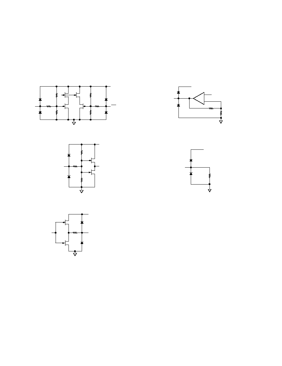
15k
30k
40
15k
30k
40
A
IN
AV
DD
A
IN
Figure 2. Analog Input Stage
2.6k
2.6k
600
ENCODE
Figure 3. Encode Inputs
40
DV
DD
DX
Figure 4. Digital Output Stage
EQUIVALENT CIRCUITS
10k
V
REF
10k
REF
AV
DD
Figure 5. REF Configured as an Output
10k
REF
AV
DD
Figure 6. REF Configured as an Input
Out-of-Range Recovery Time
Out-of-range recovery time is the time it takes for the ADC to
reacquire the analog input after a transient from 10% above
positive full scale to 10% above negative full scale, or from 10%
below negative full scale to 10% below positive full scale.
REV. D
AD9214
9
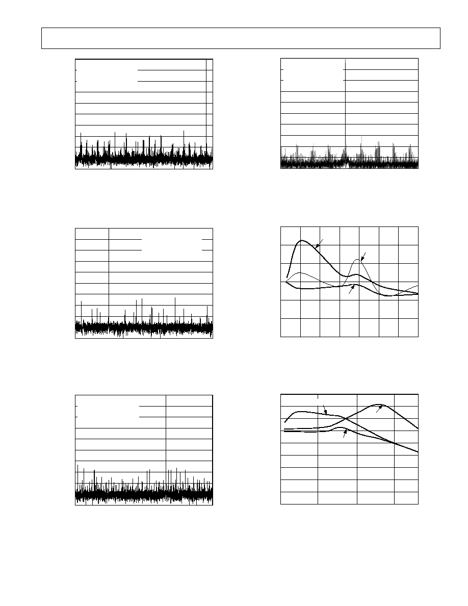
FREQUENCY MHz
0
dB
52.5
100
50
0
90
80
70
60
40
30
20
10
ENCODE: 105MSPS
A
IN
: 50.3MHz @ 0.5dBFS
SNR: 53.0dB
ENOB: 8.5 BITS
SFDR: 64dBFS
TPC 1. FFT: f
S
= 105 MSPS, f
IN
= ~50.3 MHz; A
IN
= 0.5 dBFS
Differential, 1 V p-p Analog Input Range
0
40
100
50
0
90
80
70
60
40
30
20
10
ENCODE: 80MSPS
A
IN
: 70.3MHz @ 0.5dBFS
SNR: 54.0dB
ENOB: 8.5 BITS
SFDR: 64dBFS
FREQUENCY MHz
dB
TPC 2. FFT: f
S
= 80 MSPS, f
IN
= 70 MHz; A
IN
= 0.5 dBFS,
1 V p-p Analog Input Range
FREQUENCY MHz
0
dB
52.5
100
50
0
90
80
70
60
40
30
20
10
ENCODE: 105MSPS
A
IN
: 70.3MHz @ 0.5dBFS
SNR: 52.6dB
ENOB: 8.4 BITS
SFDR: 62.6dBFS
TPC 3. FFT: f
S
= 105 MSPS; f
IN
= 70 MHz (1 V p-p)
Typical Performance Characteristics
FREQUENCY MHz
0
dB
52.5
100
50
0
90
80
70
60
40
30
20
10
ENCODE: 65MSPS
A
IN
: 15.3MHz @ 0.5dBFS
SNR: 56.9dB
ENOB: 9.2 BITS
SFDR: 70dB
TPC 4. FFT: f
S
= 65 MSPS, f
IN
= 15.3 MHz (2 V p-p) with
AD8138 Driving A
IN
A
IN
FREQUENCY MHz
0
dB
70
50
100
40
60
70
80
90
60
50
40
30
20
10
3RD
SFDR
2ND
TPC 5. Harmonic Distortion (Second and Third) and SFDR
vs. A
IN
Frequency (1 V p-p, f
S
= 105 MSPS)
A
IN
FREQUENCY MHz
0
dB
60
85
40
65
70
75
80
75
50
25
2ND
SFDR
55
50
45
3RD
TPC 6. Harmonic Distortion (Second and Third) and SFDR
vs. A
IN
Frequency (1 V p-p, f
S
= 80 MSPS)
REV. D
AD9214
10
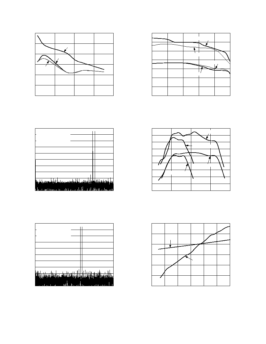
FREQUENCY MHz
0
dB
70
40
80
90
100
60
40
20
60
50
80
3RD
SFDR
2ND
TPC 7. Harmonic Distortion (Second and Third) and SFDR
vs. A
IN
Frequency (1 V p-p and 2 V p-p, f
S
= 65 MSPS)
dB
100
50
0
90
80
70
60
40
30
20
10
ENCODE: 80MSPS
A
IN
: 29.3MHz @ 6dBFS
30.3MHz @ 6dBFS
SFDR: 74dBFS
FREQUENCY MHz
0
40
TPC 8. Two-Tone Intermodulation Distortion (29.3 MHz,
30.3 MHz; 1 V p-p, f
S
= 80 MSPS)
dB
100
50
0
90
80
70
60
40
30
20
10
FREQUENCY MHz
0
52.5
ENCODE: 105MSPS
A
IN
: 30MHz @ 6dBFS
31MHz @ 6dBFS
SFDR: 73dBFS
TPC 9. Two-Tone Intermodulation Distortion (30 MHz and
31 MHz; 1 V p-p, f
S
= 105 MSPS)
ENCODE RATE MSPS
SIGNAL LEVEL
dB
80
45
75
40
55
60
65
70
60
40
20
50
SINAD 2V pp
SINAD 1V pp
SFDR 2V pp
SFDR 1V pp
100
120
TPC 10. SINAD and SFDR vs. Encode Rate (f
IN
= 10.3 MHz;
1 V p-p and 2 V p-p)
SIGNAL LEVEL
dB
45
75
55
60
65
70
50
PULSEWIDTH HIGH ns
2
4
6
8
10
40
35
30
SINAD 105MSPS
SINAD 80MSPS
SFDR 105MSPS
SFDR 80MSPS
TPC 11. SINAD and SFDR vs. Encode Pulsewidth High
(1 V p-p)
I
AVDD
mA
40
120
80
100
60
ENCODE RATE MSPS
0
20
120
20
0
I
AVDD
4
12
8
10
6
2
0
I
DrVDD
mA
40
60
80
100
I
DrVDD
TPC 12. I
AVDD
and I
DrV
DD
vs. Encode Rate (f
AIN
= 10.3 MHz,
0.5 dBFS, and 3 dBFS) C
LOAD
on Digital Outputs ~7 pF
REV. D
AD9214
11
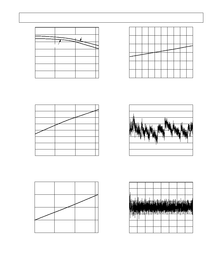
TEMPERATURE C
40
SIGNAL LEVEL
dB
46
58
44
48
50
52
54
80
40
0
56
SINAD 10.3MHz/105MSPS
SNR 10.3MHz/105MSPS
TPC 13. SINAD/SNR vs. Temperature (f
AIN
= 10.3 MHz,
f
ENCODE
= 105 MSPS, 1 V p-p)
TEMPERATURE C
40
% FULL SCALE
0.5
4.0
0.0
1.0
1.5
2.0
2.5
80
40
0
3.0
3.5
TPC 14. ADC Gain vs. Temperature (with External 1.25 V
Reference)
TEMPERATURE C
40
REFERENCE VOLTAGE
V
1.240
1.220
1.225
1.230
80
40
0
1.235
TPC 15. ADC Reference vs. Temperature (with 200
µA Load)
I
REF
A
500
V
REF
V
1.40
1.10
1.15
1.25
1.35
1.30
1.20
400 300 200 100
0
100
200
300
400
500
TPC 16. ADC Reference vs. Current Load
CODE
0
INL
LSB
1.00
1.00
0.75
0.00
0.75
0.25
0.25
128
256
384
512
640
768
896
1024
0.50
0.50
TPC 17. INL @ 80 MSPS
CODE
0
DNL
LSB
1.00
1.00
0.75
0.00
0.75
0.25
0.25
128
256
384
512
640
768
896
1024
0.50
0.50
TPC 18. DNL @ 80 MSPS
REV. D
AD9214
12
THEORY OF OPERATION
The AD9214 architecture is a bit-per-stage pipeline converter
utilizing switch capacitor techniques. These stages determine
the 7 MSBs and drive a 3-bit flash. Each stage provides suffi-
cient overlap and error correction allowing optimization of
comparator accuracy. The input buffer is differential and both
inputs are internally biased. This allows the most flexible use of
ac or dc and differential or single-ended input modes. The out-
put staging block aligns the data, carries out the error correction
and feeds the data to output buffers. The output buffers are
powered from a separate supply, allowing support of different
logic families. During power-down, the outputs go to a high
impedance state.
APPLYING THE AD9214
Encoding the AD9214
Any high-speed A/D converter is extremely sensitive to the
quality of the sampling clock provided by the user. A Track/
Hold circuit is essentially a mixer. Any noise, distortion, or
timing jitter on the clock will be combined with the desired
signal at the A/D output. For that reason, considerable care has
been taken in the design of the ENCODE input of the AD9214,
and the user is advised to give commensurate thought to the clock
source. The ENCODE input is fully TTL/CMOS compatible, and
should normally be driven directly from a low jitter, crystal-
controlled TTL/CMOS oscillator.
The ENCODE input is internally biased, allowing the user to
ac-couple in the clock signal. The cleanest clock source is often
a crystal oscillator producing a pure sine wave. Figure 7 illustrates
ac coupling such a source to the ENCODE input.
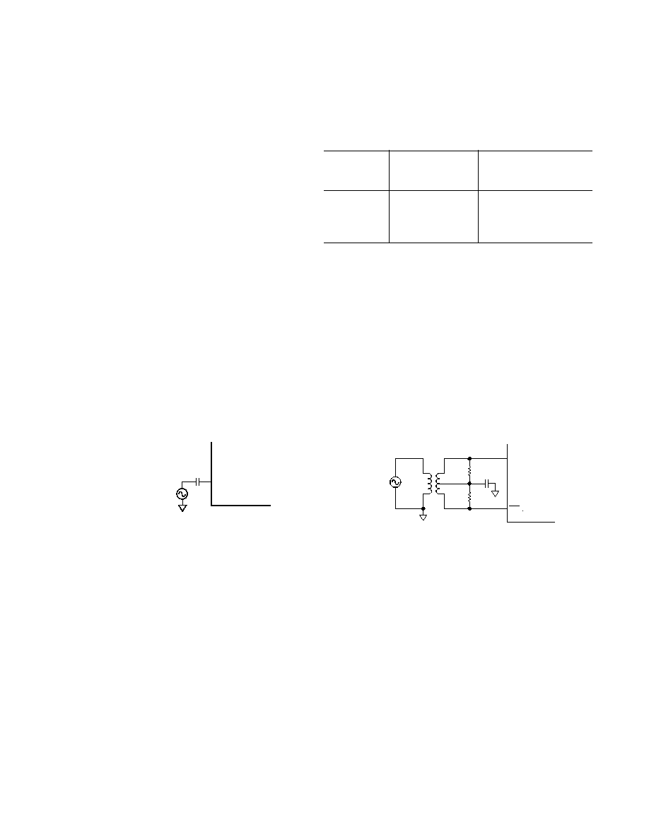
ENCODE
LOW JITTER CRYSTAL SINE OR
PULSE SOURCE 1V p-p
AD9214
Figure 7. AC-Coupled Encode Circuit
Reference Circuit
The reference circuit of the AD9214 is configured by REFSENSE
(Pin 3). By externally connecting REFSENSE to AGND, the
ADC is configured to use the internal reference (~1.25 V), and
the REF pin connection (Pin 4) is configured as an output for
the internal reference voltage.
If REFSENSE is externally connected to AV
DD
, the ADC is
configured to use an external reference. In this mode, the REF
pin is configured as a reference input, and must be driven by an
external 1.25 V reference.
In either configuration, the analog input voltage range (either
1 V p-p or 2 V p-p as determined by DFS/Gain) will track the
reference voltage linearly, and an external bypass capacitor should
be connected between REF and AGND to reduce noise on the
reference. In practice, no appreciable degradation in performance
occurs when an external reference is adjusted
±5%.
DFS/GAIN
The DFS/GAIN (Data Format Select/Gain) input (Pin 2)
controls both the output data format and gain (analog input volt-
age range) of the ADC. The table below describes its operation.
Table I. Data Format and Gain Configuration
External
Differential
DFS/GAIN
Analog Input
Connection
Voltage Range
Output Data Format
AGND
1 V p-p
Offset Binary
AV
DD
1 V p-p
Two's Complement
REF
2 V p-p
Two's Complement
Floating
2 V p-p
Offset Binary
Driving the Analog Inputs
The analog input to the AD9214 is a differential buffer. As
shown in the equivalent circuits, each of the differential inputs is
internally dc biased at ~AV
DD
/3 to allow ac-coupling of the
analog input signal. The analog signal may be dc-coupled as
well. In this case, the dc load will be equivalent to ~10 k
to
AV
DD
/3, and the dc common-mode level of the analog signals
should be within the range of AV
DD
/3
±200 mV. For best dynamic
performance, impedances at A
IN
and
AIN should match.
Driving the analog input differentially optimizes ac performance,
minimizing even order harmonics and taking advantage of
common-mode rejection of noise. A differential signal may be
transformer-coupled, as illustrated in Figure 8, or driven from a
high-performance differential amplifier such as the AD8138
illustrated in Figure 9.
A
IN
A
IN
0.1 F
25
25
1:1
50
ANALOG
SIGNAL
SOURCE
AD9214
Figure 8. Single-Ended-to-Differential Conversion Using
a Transformer
Special care was taken in the design of the analog input section
of the AD9214 to prevent damage and corruption of data when
the input is overdriven. The optimal input range is 1.0 V p-p, but
the AD9214 can support a 2.0 V p-p input range with some degra-
dation in performance (see DFS/GAIN pin description above).
REV. D
AD9214
13
AD9214
50
ANALOG
SIGNAL
SOURCE
15pF
50
50
VOCM
+
+
AD8138
500
500
500
500
0.1 F
AV
DD
10k
5k
A
IN
A
IN
Figure 9. DC-Coupled Analog Input Circuit
POWER SUPPLIES
The AD9214 has two power supplies, AV
DD
and DrV
DD
. AV
DD
and AGND supply power to all the analog circuitry, the inputs
and the internal timing and digital error correction circuits.
AV
DD
supply current will vary slightly with encode rate, as noted in
the Typical Performance Characteristics section.
DrV
DD
and DGND supply only the CMOS digital outputs,
allowing the user to adjust the voltage level to match down-
stream logic.
DrV
DD
current will vary depending on the voltage level, external
loading capacitance, and the encode frequency. Designs that mini-
mize external load capacitance will reduce power consumption
and reduce supply noise that may affect ADC performance. The
maximum DrV
DD
current can be calculated as
I
V
C
fencode
N
DrV
DrV
LOAD
DD
DD
=
×
×
×
where N is the number of output bits, 10 in the case of the
AD9214. This maximum current is for the condition of every
output bit switching on every clock cycle, which can only occur
for a full scale square wave at the Nyquist frequency, f
ENCODE
/2.
In practice, I
DrV
DD
will be the average number of output bits
switching, which will be determined by the encode rate and the
characteristics of the analog input signal. The performance
curves section provides a reference of I
DrV
DD
versus encode rate
for a 10.3 MHz sine wave driving the analog input.
Both power supply connections should be decoupled to ground
at or near the package connections, using high quality, ceramic
chip capacitors. A single ground plane is recommended for all
ground (AGND and DGND) connections.
The PWRDN control pin configures the AD9214 for a sleep
mode when it is logic HIGH. PWRDN floats logic LOW for
normal operation. In sleep mode, the ADC is not active, and
will consume less power. When switching from sleep mode to
normal operation, the ADC will need ~15 clock cycles to recover to
valid output data.
Digital Outputs
Care must be taken when designing the data receivers for the
AD9214. It is recommended that the digital outputs drive a
series resistor (e.g., 100
) followed by a gate like the 74LCX821.
To minimize capacitive loading, there should be only one gate
on each output pin. An example of this is shown in the evaluation
board schematic in Figure 10. The series resistors should be
placed as close to the AD9214 as possible to limit the amount of
current that can flow into the output stage. These switching
currents are confined between ground (DGND) and the DrV
DD
pins. Standard TTL gates should be avoided since they can
appreciably add to the dynamic switching currents of the AD9214.
It should also be noted that extra capacitive loading will increase
output timing and invalidate timing specifications. Digital output
timing is guaranteed with 10 pF loads.
LAYOUT INFORMATION
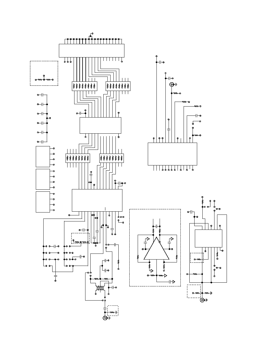
The schematic of the evaluation board (Figure 10) represents a
typical implementation of the AD9214. A multilayer board is
recommended to achieve best results. It is highly recommended
that high quality, ceramic chip capacitors be used to decouple
each supply pin to ground directly at the device. The pinout of
the AD9214 facilitates ease of use in the implementation of high
frequency, high resolution design practices. All of the digital
outputs and their supply and ground pin connections are segre-
gated to one side of the package, with the inputs on the opposite
side for isolation purposes.
Care should be taken when routing the digital output traces. To
prevent coupling through the digital outputs into the analog
portion of the AD9214, minimal capacitive loading should be
placed on these outputs. It is recommended that a fan-out of
only one gate should be used for all AD9214 digital outputs.
The layout of the encode circuit is equally critical. Any noise
received on this circuitry will result in corruption in the digitiza-
tion process and lower overall performance. The Encode clock
must be isolated from the digital outputs and the analog inputs.
EVALUATION BOARD
The AD9214 evaluation board offers designers an easy way to
evaluate device performance. The user must supply an analog
input signal, encode clock reference, and power supplies. The
digital outputs of the AD9214 are latched on the evaluation
board, and are available with a data ready signal at a 40-pin
edge connector. Please refer to the evaluation board schematic,
layout, and Bill of Materials.
Power Connections
Power to the board is supplied via three detachable, 4-pin power
strips (U4, U9, and U10). These 12 pins should be driven as
outlined in the Table II.
Table II. Power Supply Connections for AD9214
Evaluation Board
External Supply
Pin
Designator
Required
1
LVC
3 V
3
+5 V
+5 V
(Optional Z1 Supply)
5
5 V
5 V
(Optional Z1 Supply)
7
VCC
3 V
9
VDD
3 V
11
DAC
5 V
2, 4, 6,
GND
Ground
8, 10, 12
Please note that the +5 V and 5 V supplies are optional, and
only required if the user adds differential op amp Z1 to the board.

REV. D
AD9214
14
Reference Circuit
The evaluation board is configured at assembly to use the
AD9214's on-board reference. To supply an external reference,
the user must connect the REFSENSE pin to VCC by removing
the jumper block connecting E25 to E26, and placing it between
E19 and E24. In this configuration, an external 1.25 V reference
must be connected to jumper connection E23. Jumper connections
E19E21, E24, and resistors R13R14 are omitted at assembly,
and not used in the evaluation of the AD9214.
Gain/Data Format
The evaluation board is assembled with the DFS/GAIN pin
connected to ground; this configures the AD9214 for a 1 V p-p
analog input range, and offset binary data format. The user may
remove this jumper and replace it to make one of the connections
described in the table below to configure the AD9214 for different
gain and output data format options.
Table III. Data Format and Gain Configuration for
Evaluation Board
DFS/GAIN
Jumper
DFS/GAIN
Differential Output Data
Placement
Connection
A
IN
Range
Format
E18 to E12
AGND
1 V p-p
Offset Binary
E16 to E11
AV
DD
1 V p-p
Two's Complement
E15 to E14
REF
2 V p-p
Two's Complement
E17 to E13
Floating
2 V p-p
Offset Binary
Power-Down
The evaluation board is configured at assembly so that the
PWRDN input floats low for normal operating condition. The
user may add a jumper between option holes E5 and E6 to
connect PWRDN to AVCC, configuring the AD9214 for power-
down mode.
Encode Signal and Distribution
The encode input signal should drive SMB connector J5, which
has an on-board 50
termination. A standard CMOS compatible
pulse source is recommended. Alternatively, the user can adjust
the dc level of an ac-coupled clock source by adding resistor
R11, normally omitted. J5 drives the AD9214 ENCODE input
and one gate of U12, which buffers and distributes the clock
signal to the on-board latch (U3), the reconstruction DAC
(U11), and the output data connector (U2). The board comes
assembled with timing options optimized for the DAC and latch;
the user may invert the DR signal at Pin 37 of edge connector
U2 by removing the jumper block between E34 and E35, and
reinstalling it between E35 and E36.
Analog Input
The analog input signal is connected to the evaluation board by
SMB connector J1. As configured at assembly, the signal is ac
coupled by capacitor C10 to transformer T1. This 1:1 transformer
provides a 50
termination for connector J1 via 25 resistors
R1 and R4. T1 also converts the signal at J1 into a differential
signal for the analog inputs of the AD9214. Resistor R3, normally
omitted, can be used to terminate J1 if the transformer is removed.
The user can reconfigure the board to drive the AD9214 single-
endedly by removing the jumper block between E1 and E3, and
replacing it between E3 and E2. In this configuration, capacitor
C2 stabilizes the self-bias of
AIN, and resistor R2 provides a
matched impedance for a 50
source at J1.
Transformer T1 can be bypassed by moving the jumper normally
between E40 and E38 to connect E40 to E37, and moving the
jumper normally between E39 and E10 to connect E7 to E10.
In this configuration, the analog input of the AD9214 is driven
single ended, directly from J1; and R3 (normally omitted) should
be installed to terminate any cable connected to J1.
Using the AD8138
An optional driver circuit for the analog input, based on the
AD8138 differential amplifier, is included in the layout of the
AD9214 evaluation board. This portion of the evaluation circuit
is not populated when the board is manufactured, but can be
easily be added by the user. Resistors R5, R16, R18, and R25
are the feedback network that sets the gain of the AD8138.
Resistors R23 and R24 set the common-mode voltage at the
output of the op amp. Resistors R27 and R28, and capacitor
C15, form a low-pass filter at the output of the AD8138, limiting
its noise contribution into the AD9214.
Once the drive circuit is populated, the user should remove the
jumper block normally between E40 and E38, and place it between
E40 and E41. This will ac-couple the analog input signal from
SMB connector J1 to the AD8138 drive circuit. The user will also
need to remove the jumper blocks that normally connect E39 to
E10 and E1 to E3 to remove transformer T1 from the circuit.
DAC Reconstruction Circuit
The data available at output connector U2 is also reconstructed by
DAC U11, the AD9752. This 12-bit, high-speed digital-to-analog
converter is included as a tool in setting up and debugging the
evaluation board. It should not be used to measure the per-
formance of the AD9214, as its performance will not accurately
reflect the performance of the ADC. The DAC's output, available
at J2, will drive 50
. The user can add a jumper block between
E8 and E9 to activate the SLEEP function of the DAC.

REV. D
AD9214
15
AD9214/PCB Bill of Material
#
Quantity
Reference Designator
Device
Package
Value
1
1
N/A
PCB
2
19
C1C3, C5C14, C16C20, C25C28
Capacitor
603
0.1
µF
3
4
C21C24
Capacitor
CAPTAJD
10
µF
4
1
C4
Capacitor
603
0.01
µF
5
4
R1, R2, R4, R8
Resistor
1206
25
6
4
R7, R10, R12, R17
Resistor
1206
50
7
4
U5U8
Resistor
RPAK_742
100
8
1
R21
Resistor
1206
0
9
2
R6, R9
Resistor
1206
2000
10
37
E1E6, E8E9, E11E27, E29, E31E41
Test Points
TSW-120-07-G-S
Jumper Connections
SMT-100-BK-G
11
3
J1, J2, J5
Connector
SMB
51-52-220
12
1
U12
Clock Chip
SOIC
SN74LVC86
13
1
U11
DAC
SOIC
AD9752
14
1
U3
Latch
SOIC
74LCX821
15
1
U1
ADC/DUT
SOIC
AD9214
16
1
U2
40-Pin Header
Samtec TSW-120-07-G-D
17
1
T1
Transformer
Mini Circuits ADT1-1WT
18
3
U4, U9, U10
Power Strip
Newark 95F5966
Power Connector
25.602.5453.0
The following items are included in the PCB design, but are omitted at assembly.
19
3
C1, C20, C28
Capacitor
603
0.1
µF
20
2
C30, C29
Capacitor
CAPTAJD
10
µF
21
1
C15
Capacitor
603
15 pF
22
4
R5, R18, R25, R26
Resistor
1206
500
23
1
R23
Resistor
1206
1 k
24
1
R24
Resistor
1206
4 k
25
3
R11, R15, R16
Resistor
1206
User Select
26
2
R13, R14
Resistor
1206
N/A
27
3
R27, R28, R3
Resistor
1206
50
28
1
R19
Resistor
1206
0
29
1
Z1
Op Amp
SOIC
AD8138
REV. D
AD9214
16
34
32
30
28
26
24
C3
0.1
F
C7
0.1
F
V
CC
V
CC
GND
GND
AMP
AMP
E3
E1
E2
C2
0.1
F
GND
C8
0.1
F
ENC
E4
E5
E6
GND
V
CC
1
2
3
4
5
6
7
8
9
10
11
12
13
14
28
27
26
25
24
23
22
21
20
19
18
17
16
15
GND
C9
0.1
F
V
DD
GND
V
DD
GND
1
2
3
4
5
6
7
8
16
15
14
13
12
11
10
9
APAK_742
1
2
3
4
5
6
7
8
16
15
14
13
12
11
10
9
APAK_742
GND
GND
1
2
3
4
5
6
7
8
9
10
11
12
24
23
22
21
20
19
18
17
16
15
14
13
V
DD
1
2
3
4
5
6
7
8
16
15
14
13
12
11
10
9
APAK_742
U7
1
2
3
4
5
6
7
8
16
15
14
13
12
11
10
9
C19
0.1
F
CLKLAT
D9
MSB
D8
D7
D6
D5
E30
DTR
LVC
3V
GND
+
5V
GND
1
234
5V
GND
V
CC
3V
GND
1
234
V
DD
3V
GND
DAC
GND
1
234
U9
U4
U10
C30
10
F
C29
10
F
C21
10
F
C22
10
F
C23
10
F
C24
10
F
5V
+5V
L
VC
V
CC
V
DD
DAC
GND
GND
V
DD
CLKLAT
R16
50
R15
50
OPTIONAL
GND
E14
E15
V
CC
E11
E16
E12
E18
E13
E17
C17
0.1
F
C26
0.1
F
GND
GND
GND
E23
E22
V
CC
E24
E19
E26
E25
E20
E21
GND
GND
C25
0.1
F
R13
2k
R14
2k
OPTIONAL
GND
C27
0.1
F
E39
E7
E10
R4
25
R1
25
C4
0.1
F
C6
0.1
F
GND
G
ND
1
5
3
6
2
4
GND
E37
E40
E38
C10
0.1
F
E29
R3
50
OPTIONAL
C18
0.1
F
GND
GND
R2
25
0.1
F
C8
OR
DFS/GAIN
REFSENSE
REF
AGND1
AV
DD
AV
DD
AGND
A
IN
A
IN
AGND
AV
DD
CLK
PWRDN
D9
MSB
D8
D7
D6
DrV
DD
DGND
D5
D4
D3
D2
D1
D0
LSB
DrV
DD
1
DGND1
AD9214A
U1
U7
U8
DE
D9
D8
D7
D6
D5
D4
D3
D2
D1
D0
GND
V
CC
D9
D8
D7
D6
D5
D4
D3
D2
D1
D0
CLK
74LCXB21
U3
APAK_742
U8
T1
R12
50
J5
LVC
R11
50
ENC
R21
0
R19
0
1
2
3
4
5
6
7
GND
GND
1A
1B
1Y
2A
2B
2Y
GND
5N74LVC86
U12
R17
50
DR
E35
E34
GND
E36
LVC
ENC
OPTIONAL
14
13
12
11
10
9
8
V
CC
4B
4A
4Y
3B
3A
3Y
CLKDAC
E33
E31
GND
E32
LVC
CLKLAT
LVC
E27
E28
GND
R10
50
LVC
GND
C16
0.1
F
J1
10
11
12
13
14
28
27
26
25
24
23
22
21
20
19
18
17
16
15
D9
MSB
D8
D7
D6
D5
D4
D3
D2
D1
D0
LSB
GND
GND
GND
CLKDAC
GND
GND
1
2
3
4
5
6
7
8
9
DB11
DB10
DB9
DB8
DB7
DB6
DB5
DB4
DB3
DB2
DB1
DB0
NC1
NC2
CLK
DVDD
DCOM
NC3
AVDD
ICOMP
IOUTA
IOUTB
ACOM
NC4
FSADJ
REFIO
REFLO
SLEEP
AD9752
U11
E9
E8
R6
2k
GND
DAC
GND
C12
0.1
F
R9
2k
GND
R8
25
GND
R7
50
GND
J2
GND
C11
0
.1
F
GND
C13
0.1
F
DAC
GND
C14
0.1
F
DAC
GND
39
37
35
33
31
29
27
25
23
21
19
17
GND
DR
GND
13
11
9
7
5
3
1
15
40
38
36
22
20
18
16
14
12
10
8
6
4
2
GND
37
35
33
31
29
27
25
23
21
19
17
39
13
11
9
7
5
3
1
15
40
38
36
34
32
30
28
26
24
22
20
18
16
14
12
10
8
6
4
2
4QPHA
U2
D4
D3
D2
D1
D0
OPTIONAL
R26
500
6
5
4
3
C20
0.1
F
5V
AD8138
R25
500
VCOM
1
2
8
R25
4k
R23
1k
5V
C1
0.1
F
R5
500
R18
500
E41
C28
0.1
F
V
V
R28
50
R27
50
C15
15pF
AMP
AMP
Z1
5V
GND
V
CC
OPTIONAL
Figure 10. PCB Schematic

REV. D
AD9214
17
Figure 11. PCB Top Side Silkscreen
\
Figure 12. PCB Top Side Copper
Figure 13. PCB Bottom Side Silkscreen
Figure 14. PCB Bottom Side Copper
Figure 15. PCB Ground Layer--Layer TBD
Figure 16. PCB Power Layers--Layers 3 and 4
REV. D
AD9214
18
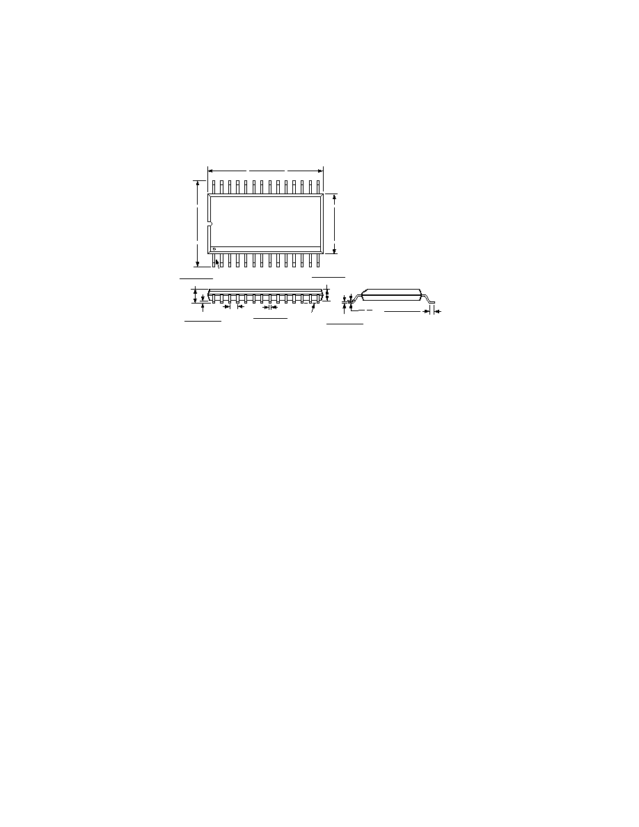
OUTLINE DIMENSIONS
Dimensions shown in inches and (mm).
28-Lead Shrink Small Outline Package
(RS-28)
0.009 (0.229)
0.005 (0.127)
0.03 (0.762)
0.022 (0.558)
8°
0°
0.008 (0.203)
0.002 (0.050)
0.07 (1.79)
0.066 (1.67)
0.078 (1.98)
0.068 (1.73)
0.015 (0.38)
0.010 (0.25)
SEATING
PLANE
0.0256
(0.65)
BSC
0.311 (7.9)
0.301 (7.64)
0.212 (5.38)
0.205 (5.21)
28
15
14
1
0.407 (10.34)
0.397 (10.08)
PIN 1
CONTROLLING DIMENSIONS ARE IN MILLIMETERS; INCH DIMENSIONS
ARE ROUNDED-OFF MILLIMETER EQUIVALENTS FOR REFERENCE
ONLY AND ARE NOT APPROPRIATE FOR USE IN DESIGN

REV. D
AD9214
19
Revision History
Location
Page
Data Sheet changed from REV. C to REV. D.
Edit to Functional Block Diagram . . . . . . . . . . . . . . . . . . . . . . . . . . . . . . . . . . . . . . . . . . . . . . . . . . . . . . . . . . . . . . . . . . . . . . . . . . . 1
TPC 15 replaced with new figure . . . . . . . . . . . . . . . . . . . . . . . . . . . . . . . . . . . . . . . . . . . . . . . . . . . . . . . . . . . . . . . . . . . . . . . . . . 11
Edit to Figure 10 . . . . . . . . . . . . . . . . . . . . . . . . . . . . . . . . . . . . . . . . . . . . . . . . . . . . . . . . . . . . . . . . . . . . . . . . . . . . . . . . . . . . . . . 16
07/01--Data Sheet changed from REV. B to REV. C.
Edit to ABSOLUTE MAXIMUM RATINGS . . . . . . . . . . . . . . . . . . . . . . . . . . . . . . . . . . . . . . . . . . . . . . . . . . . . . . . . . . . . . . . . . 5
05/01--Data Sheet changed from REV. A to REV. B.
Changes to PSRR Specifications in AD9214-65, AD9214-80, AD9214-105 Columns . . . . . . . . . . . . . . . . . . . . . . . . . . . . . . . . . . . 2
Change to SNR Specifications in AD9214-105 Column . . . . . . . . . . . . . . . . . . . . . . . . . . . . . . . . . . . . . . . . . . . . . . . . . . . . . . . . . . 3
Changes to THIRD HARMONIC DISTORTION Specifications in AD9214-105 Column . . . . . . . . . . . . . . . . . . . . . . . . . . . . . . . 3
01/01--Data Sheet changed from REV. 0 to REV. A.
Changes to DC Specifications in AD9214-65, AD9214-80, AD9214-105 Columns . . . . . . . . . . . . . . . . . . . . . . . . . . . . . . . . . . . . . 2
Changes to AC Specifications in AD9214-65, AD9214-105 Columns . . . . . . . . . . . . . . . . . . . . . . . . . . . . . . . . . . . . . . . . . . . . . . . 3

20
C0169302/02(D)
PRINTED IN U.S.A.