 | ÐлекÑÑоннÑй компоненÑ: AD9218 | СкаÑаÑÑ:  PDF PDF  ZIP ZIP |
Äîêóìåíòàöèÿ è îïèñàíèÿ www.docs.chipfind.ru
REV. 0
Information furnished by Analog Devices is believed to be accurate and
reliable. However, no responsibility is assumed by Analog Devices for its
use, nor for any infringements of patents or other rights of third parties that
may result from its use. No license is granted by implication or otherwise
under any patent or patent rights of Analog Devices.
a
AD9218
One Technology Way, P.O. Box 9106, Norwood, MA 02062-9106, U.S.A.
Tel: 781/329-4700
www.analog.com
Fax: 781/326-8703
© Analog Devices, Inc., 2001
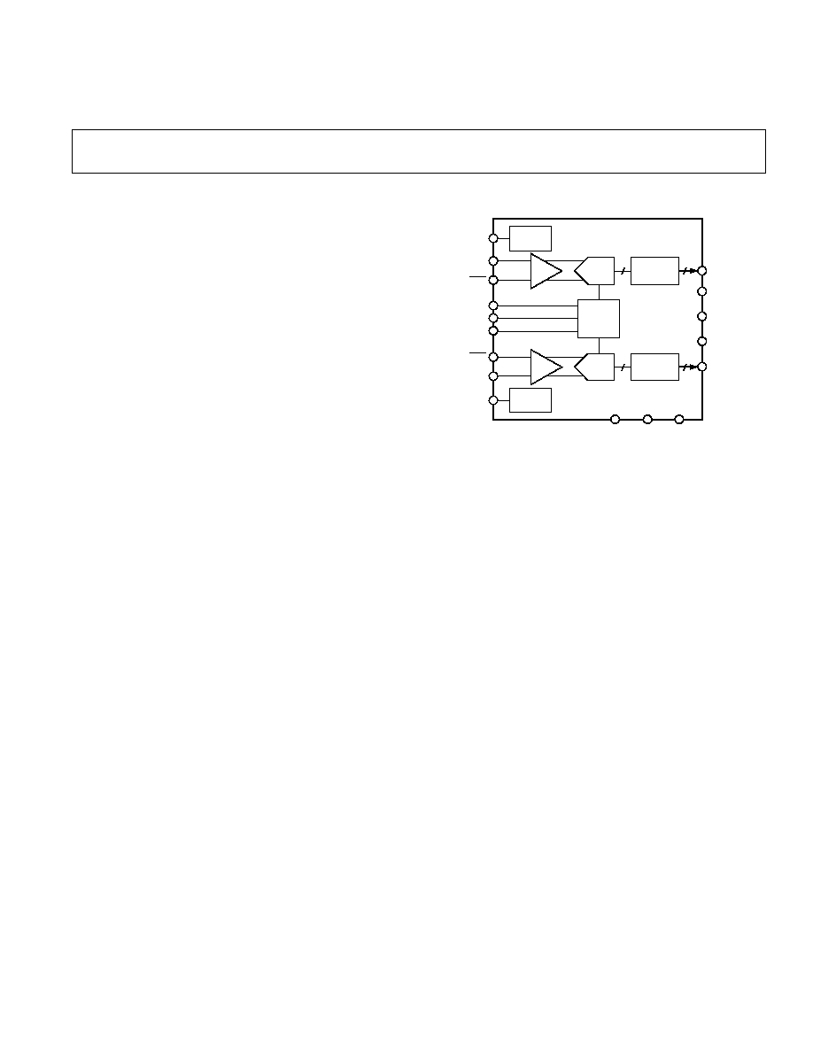
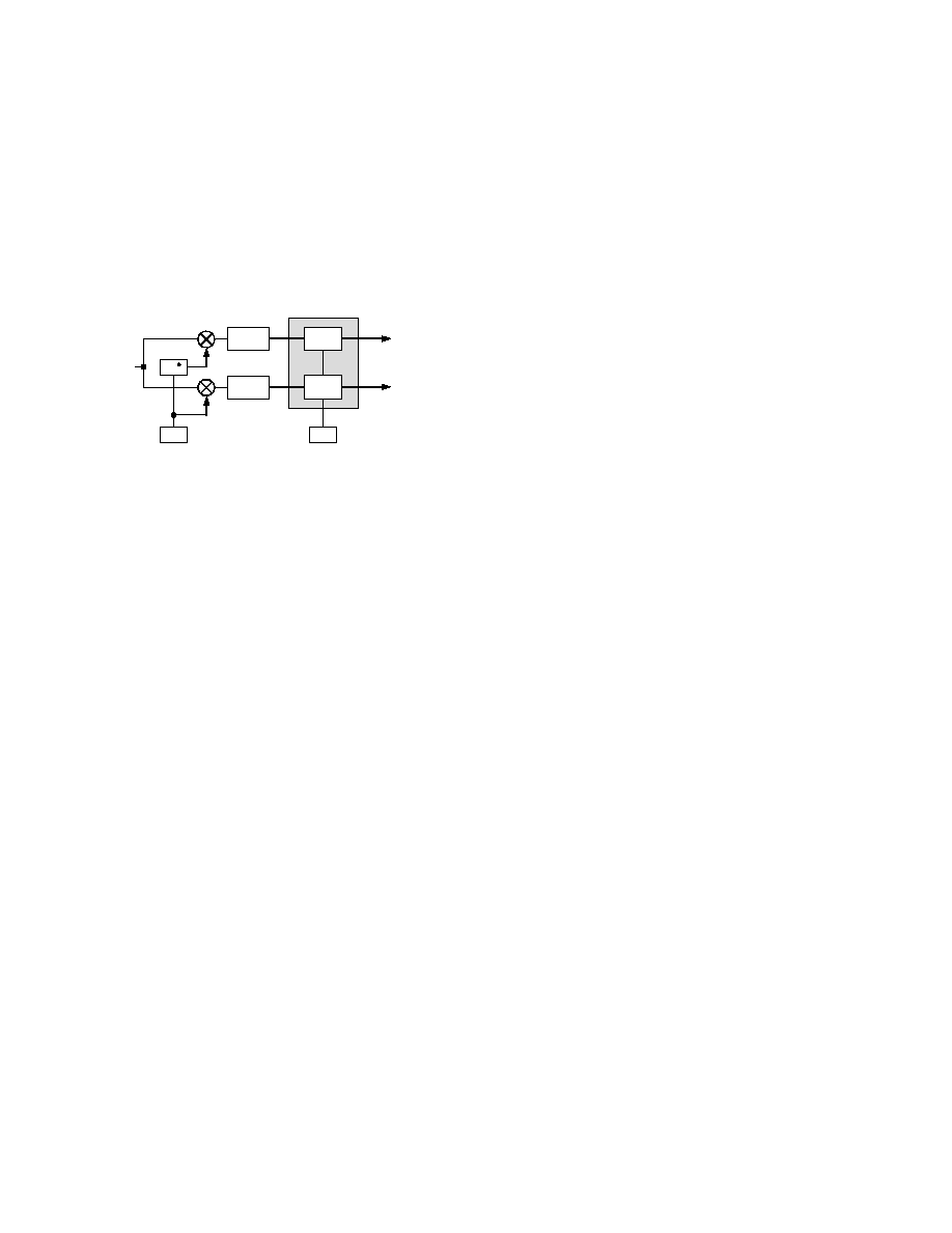
FUNCTIONAL BLOCK DIAGRAM
10-Bit, 40/65/80/105 MSPS
3 V Dual A/D Converter
FUNCTIONAL BLOCK DIAGRAM
TIMING
ADC
OUTPUT
REGISTER
REF
T/H
10
10
ADC
OUTPUT
REGISTER
T/H
10
10
TIMING
USER
SELECT #1
USER
SELECT #2
DATA
FORMAT/
GAIN
D
9B
D
0B
D
9A
D
0A
V
DD
GND
V
D
AD9218
ENCODE A
ENCODE B
A
IN
B
A
IN
A
A
IN
A
REF
IN
A
REF
IN
B
REF
OUT
A
IN
B
FEATURES
Dual 10-Bit, 40 MSPS, 65 MSPS, 80 MSPS, and
105 MSPS ADC
Low Power: 275 mW at 105 MSPS per Channel
On-Chip Reference and Track/Holds
300 MHz Analog Bandwidth Each Channel
SNR = 57 dB @ 41 MHz, Encode = 80 MSPS
1 V p-p or 2 V p-p Analog Input Range Each Channel
Single 3.0 V Supply Operation (2.7 V3.6 V)
Power-Down Mode for Single Channel Operation
Two's Complement or Offset Binary Output Mode
Output Data Alignment Mode
Pin-Compatible with 8-Bit AD9288
75 dBc Crosstalk between Channels
APPLICATIONS
Battery-Powered Instruments
Hand-Held Scopemeters
Low Cost Digital Oscilloscopes
I and Q Communications
Ultrasound Equipment
GENERAL DESCRIPTION
The AD9218 is a dual 10-bit monolithic sampling analog-to-
digital converter with on-chip track-and-hold circuits and is
optimized for low cost, low power, small size and ease of use.
The product operates at a 105 MSPS conversion rate with
outstanding dynamic performance over its full operating range.
Each channel can be operated independently.
The ADC requires only a single 3.0 V (2.7 V to 3.6 V) power
supply and an encode clock for full operation. No external
reference or driver components are required for many applica-
tions. The digital outputs are TTL/CMOS-compatible and a
separate output power supply pin supports interfacing with
3.3 V or 2.5 V logic.
The clock input is TTL/CMOS-compatible and the 10-bit
digital outputs can be operated from 3.0 V (2.5 V to 3.6 V)
supplies. User-selectable options are available to offer a combi-
nation of power-down modes, digital data formats and digital
data timing schemes. In power-down mode, the digital outputs
are driven to a high-impedance state.
Fabricated on an advanced CMOS process, the AD9218 is
available in a 48-lead surface-mount plastic package (7
× 7 mm
LQFP) specified over the industrial temperature range (40
°C
to +85
°C).
PRODUCT HIGHLIGHTS
Low Power--Just 275 mW power dissipation per channel at
105 MSPS. Other speed grade proportionally scaled down while
maintaining high ac performance.
Pin Compatibility Upgrade--Allows easy migration from 8-bit
to 10-bit. Pin-compatible with the 8-bit AD9288 dual ADC.
Ease of Use--On-chip reference and user controls provide flex-
ibility in system design.
High Performance--Maintain 54 dB SNR at 105 MSPS with a
Nyquist input.
Channel Crosstalk--Very low at 75 dBc.

REV. 0
2
AD9218SPECIFICATIONS
DC SPECIFICATIONS
Test
AD9218BST-40/-65
AD9218BST-80/-105
Parameter
Temp
Level
Min
Typ
Max
Min
Typ
Max
Unit
RESOLUTION
10
10
Bits
ACCURACY
No Missing Codes
1
Full
VI
GNT
GNT
Offset Error
2
25
°C
I
18
2
18
18
2
18
LSB
Gain Error
2
25
°C
I
2
3
8
2
3.5
8
% FS
Differential Nonlinearity
25
°C
I
1
±0.3/±0.6 1/1.3
1
±0.5/±0.8 1.2/1.7
LSB
(DNL)
Full
VI
±0.8
±0.6/±0.9
LSB
Integral Nonlinearity (INL)
25
°C
I
1/1.6
±0.3/±1
1/1.6
1.35/2.7
±0.75/±2
1.35/2.7
LSB
Full
VI
±1
±1/±2.3
LSB
TEMPERATURE DRIFT
Offset Error
Full
V
10
4
ppm/
°C
Gain Error
2
Full
V
80
100
ppm/
°C
Reference
Full
V
40
40
ppm/
°C
REFERENCE
Internal Reference Voltage
25
°C
I
1.18
1.24
1.28
1.18
1.24
1.28
V
(REFOUT)
Input Resistance (REFIN A, B)
Full
V
9
11
13
9
11
13
k
ANALOG INPUTS
Differential Input Voltage
Full
V
1 or 2
1
V
Range (AIN,
AIN)
3
Common-Mode Voltage
Full
V
V
D
/3
V
D
/3
V
Input Resistance
Full
VI
8
10
14
8
10
14
k
Input Capacitance
25
°C
V
3
3
pF
POWER SUPPLY
V
D
Full
IV
2.7
3
3.6
2.7
3
3.6
V
V
DD
Full
IV
2.7
3
3.6
2.7
3
3.6
V
Supply Currents
IV
D
(V
D
= 3.0 V)
4
Full
VI
108/117
113/122
172/183
175/188
mA
IV
DD
(V
DD
= 3.0 V)
4
25
°C
V
7/11
13/17
mA
Power Dissipation DC
5
Full
VI
325/350
340/365
515/550
525/565
mW
IV
D
Power-Down Current
6
Full
VI
20
22
mA
Power Supply Rejection Ratio
25
°C
I
±1
±1
mV/V
NOTES
1
No Missing Codes across industrial temperature range guaranteed for -40 MSPS, -65 MSPS, and -80 MSPS grades. No missing codes at room temperature guaran-
teed for -105 grade.
2
Gain error and gain temperature coefficients are based on the ADC only (with a fixed 1.25 V external reference) -65 Grade in 2 V p-p range, -40, -85, -105 Grades in
1 V p-p range.
3
(AIN
AIN) =
±0.5 V in 1 V range (full scale), (AIN AIN) = ± 1 V in 2 V range (full scale).
4
AC Power Dissipation measured with rated encode and a 10.3 MHz analog input @ 0.5 dBFS, C
LOAD
= 5 pF.
5
DC Power Dissipation measured with rated encode and a dc analog input (Outputs Static, IV
DD
= 0)
6
In power-down state IV
DD
=
± 10 µA typical (all grades).
Specifications subject to change without notice.
(V
DD
= 3.0 V, V
D
= 3.0 V; external reference, unless otherwise noted.)

REV. 0
3
AD9218
DIGITAL SPECIFICATIONS
Test
AD9218BST-40/-65
AD9218BST-80/-105
Parameter
Temp Level
Min
Typ
Max
Min
Typ
Max
Unit
DIGITAL INPUTS
Encode Input Common Mode
Full
V
V
D
/2
V
D
/2
V
Encode "1" Voltage
Full
VI
2
2
V
Encode "0" Voltage
Full
VI
0.8
0.8
V
Encode Input Resistance
Full
VI
1.8
2.0
2.3
1.8
2.0
2.3
k
Logic "1" Voltage--S1, S2, DFS
Full
VI
2
2
V
Logic "0" Voltage--S1, S2, DFS
Full
VI
0.8
0.8
V
Logic "1" Current--S1
Full
VI
50
±10
+50
50
±10
+50
µA
Logic "0" Current--S1
Full
VI
400
230
50
400
230
50
µA
Logic "1" Current--S2
Full
VI
50
230
400
50
230
400
µA
Logic "0" Current--S2
Full
VI
50
±10
+50
50
±10
+50
µA
Logic "1" Current--DFS
Full
VI
30
100
200
30
100
200
µA
Logic "0" Current--DFS
Full
VI
400
230
50
400
230
50
µA
Input Capacitance--S1, S2, Encode Inputs
25
°C V
2
2
pF
Input Capacitance DFS
25
°C V
4.5
4.5
pF
DIGITAL OUTPUTS
Logic "1" Voltage
Full
VI
2.45
2.45
V
Logic "0" Voltage
Full
VI
0.05
0.05
V
Output Coding
Two's Comp. or Offset Binary
Two's Comp. or Offset Binary
Specifications subject to change without notice.
AC SPECIFICATIONS
Test
AD9218BST-40/-65
AD9218BST-80/-105
Parameter
Temp
Level
Min
Typ
Max
Min
Typ
Max
Unit
DYNAMIC PERFORMANCE
1
Signal-to-Noise Ratio (SNR)
(Without Harmonics)
f
IN
= 10.3 MHz
25
°C
I
58/55
59/57
57/53
58/55
dB
f
IN
= Nyquist
2
25
°C
I
-/54
59/56
55/52
57/54
dB
Signal-to-Noise Ratio (SINAD)
(With Harmonics)
f
IN
= 10.3 MHz
25
°C
I
58/54
59/56
56/52
58/53
dB
f
IN
= Nyquist
2
25
°C
I
-/53
59/55
55/51
57/53
dB
Effective Number of Bits
f
IN
= 10.3 MHz
25
°C
I
9.4/8.8
9.6/9.1
9.1/8.4
9.4/8.6
Bits
f
IN
= Nyquist
2
25
°C
I
-/8.6
9.6/8.9
9/8.3
9.3/8.6
Bits
Second Harmonic Distortion
f
IN
= 10.3 MHz
25
°C
I
72/66
89/77
69/60
77/68
dBc
f
IN
= Nyquist
2
25
°C
I
-/63
89/72
65/57
76/66
dBc
Third Harmonic Distortion
f
IN
= 10.3 MHz
25
°C
I
68/62
79/68
62/57
71/63
dBc
f
IN
= Nyquist
2
25
°C
I
-/60
78/64
63/57
73/69
dBc
Spurious Free Dynamic Range SFDR
f
IN
= 10.3 MHz
25
°C
I
68/62
79/67
62/57
69/62
dBc
f
IN
= Nyquist
2
25
°C
I
-/60
78/64
63/57
70/63
dBc
Two-Tone Intermod Distortion (IMD)
f
IN1
= 10 MHz, f
IN2
= 11 MHz
25
°C
V
74/73
dBc
at 7 dBFS
f
IN1
= 30 MHz, f
IN2
= 31 MHz
25
°C
V
73/73
77/67
dBc
at 7 dBFS
Analog Bandwidth, Full Power
25
°C
V
300
300
MHz
Crosstalk
25
°C
V
75
75
dBc
NOTES
1
AC specs based on an analog input voltage of 0.5 dBFS at 10.3 MHz unless otherwise noted. AC specs for -40, -80, -105 grades are tested in 1 V p-p range and
driven differentially. AC specs for -65 grade are tested in 2 V p-p range and driven differentially.
2
The -65, -80, and -105 grades are tested close to Nyquist for that grade: 31 MHz, 39 MHz, and 51 MHz for the -65, -80, and -105 grades respectively.
Specifications subject to change without notice.
(V
DD
= 3.0 V, V
D
= 3.0 V; external reference, unless otherwise noted.)
(V
DD
= 3.0 V, V
D
= 3.0 V; external reference, unless otherwise noted.)
REV. 0
4
AD9218SPECIFICATIONS
SWITCHING SPECIFICATIONS
Test
AD9218BST-40/-65
AD9218BST-80/-105
Parameter
Temp
Level
Min
Typ
Max
Min
Typ
Max
Unit
ENCODE INPUT PARAMETERS
Maximum Encode Rate
Full
VI
40/65
80/105
MSPS
Minimum Encode Rate
Full
IV
20/20
20/20
MSPS
Encode Pulsewidth High (t
EH
)
Full
IV
7/6
5/3.8
ns
Encode Pulsewidth Low (t
EL
)
Full
IV
7/6
5/3.8
ns
Aperture Delay (t
A
)
25
°C
V
2
2
ns
Aperture Uncertainty (Jitter)
25
°C
V
3
3
ps rms
DIGITAL OUTPUT PARAMETERS
Output Valid Time (t
V
)
*
Full
VI
3
3
ns
Output Propagation Delay (t
PD
)
*
Full
VI
4.5
7
4.5
6
ns
Output Rise Time (t
R
)
25
°C
V
1
1.0
ns
Output Fall Time (t
F
)
25
°C
V
1.2
1.2
ns
Out of Range Recovery Time
25
°C
V
5
5
ns
Transient Response Time
25
°C
V
5
5
ns
Recovery Time from Power-Down
25
°C
V
10
10
Cycles
Pipeline Delay
Full
IV
5
5
Cycles
NOTES
*t
V
and t
PD
are measured from the 1.5 level of the ENCODE input to the 50%/50% levels of the digital outputs swing. The digital output load during test is not to
exceed an ac load of 5 pF or a dc current of
±40 µA. Rise and fall times measured from 10% to 90%.
Specifications subject to change without notice.
SAMPLE N
A
IN
A,
A
IN
B
ENCODE
A&B
D
9A
D
0A
D
9B
D
0B
DATA N5
SAMPLE
N+1
t
PD
SAMPLE
N+2
SAMPLE
N+3
SAMPLE
N+4
SAMPLE
N+5
SAMPLE
N+6
DATA N4
DATA N3
DATA N2
DATA N1
DATA N
DATA N5
DATA N4
DATA N3
DATA N2
DATA N1
DATA N
t
V
1/f
S
t
EL
t
EH
t
A
Figure 1. Normal Operation, Same Clock (S1 = 1, S2 = 0) Channel Timing
(V
DD
= 3.0 V, V
D
= 3.0 V; external reference, unless otherwise noted.)
REV. 0
AD9218
5
SAMPLE
N
D
9A
D
0A
D
9B
D
0B
SAMPLE
N+1
t
PD
SAMPLE
N+2
SAMPLE
N+3
SAMPLE
N+4
SAMPLE
N+5
SAMPLE
N+6
t
V
1/f
S
t
EL
t
EH
t
A
DATA N10
DATA N8
DATA N6
DATA N4
DATA N2
DATA N
DATA N+2
DATA N9
DATA N7
DATA N5
DATA N3
DATA N1
DATA N+1
ENCODE A
ENCODE B
A
IN
A,
A
IN
B
SAMPLE
N+7
SAMPLE
N+8
Figure 2. Normal Operation with Two Clock Sources (S1 = 1, S2 = 0) Channel Timing
SAMPLE
N
D
9A
D
0A
D
9B
D
0B
SAMPLE
N+1
t
PD
SAMPLE
N+2
SAMPLE
N+3
SAMPLE
N+4
SAMPLE
N+5
SAMPLE
N+6
t
V
1/f
S
t
EL
t
EH
t
A
DATA N10
DATA N8
DATA N6
DATA N4
DATA N2
DATA N
DATA N+2
ENCODE A
ENCODE B
A
IN
A,
A
IN
B
SAMPLE
N+7
SAMPLE
N+8
DATA N11
DATA N9
DATA N7
DATA N5
DATA N3
DATA N1
DATA N+1
Figure 3. Data Align with Two Clock Sources (S1 = 1, S2 = 1) Channel Timing
REV. 0
AD9218
6
CAUTION
ESD (electrostatic discharge) sensitive device. Electrostatic charges as high as 4000 V readily
accumulate on the human body and test equipment and can discharge without detection. Although
the AD9218 features proprietary ESD protection circuitry, permanent damage may occur on
devices subjected to high-energy electrostatic discharges. Therefore, proper ESD precautions are
recommended to avoid performance degradation or loss of functionality.
WARNING!
ESD SENSITIVE DEVICE
ABSOLUTE MAXIMUM RATINGS
1
V
D
, V
DD
. . . . . . . . . . . . . . . . . . . . . . . . . . . . . . . . . . . . . . . 4 V
Analog Inputs . . . . . . . . . . . . . . . . . . . . 0.5 V to V
D
+ 0.5 V
Digital Inputs . . . . . . . . . . . . . . . . . . . 0.5 V to V
DD
+ 0.5 V
REF
IN
Inputs . . . . . . . . . . . . . . . . . . . . . 0.5 V to V
D
+ 0.5 V
Digital Output Current . . . . . . . . . . . . . . . . . . . . . . . . . 20 mA
Operating Temperature . . . . . . . . . . . . . . . . 55
°C to +125°C
Storage Temperature . . . . . . . . . . . . . . . . . . 65
°C to +150°C
Maximum Junction Temperature . . . . . . . . . . . . . . . . . 150
°C
Maximum Case Temperature . . . . . . . . . . . . . . . . . . . . 150
°C
JA
2
. . . . . . . . . . . . . . . . . . . . . . . . . . . . . . . . . . . . . . . 57
°C/W
NOTES
1
Stresses above those listed under Absolute Maximum Ratings may cause perma-
nent damage to the device. This is a stress rating only; functional operation of the
device at these or any other conditions outside of those indicated in the operation
sections of this specification is not implied. Exposure to absolute maximum ratings
for extended periods may affect device reliability.
2
Measured on a four-layer board with solid ground plane.
EXPLANATION OF TEST LEVELS
Test Level
I
100% production tested.
II
100% production tested at 25
°C and sample tested at speci-
fied temperatures.
III Sample tested only.
IV Parameter is guaranteed by design and characterization testing.
V
Parameter is a typical value only.
VI 100% production tested at 25
°C; guaranteed by design
and characterization testing for industrial temperature
range; 100% production tested at temperature extremes
for military devices.
Table I. User Select Modes
S1
S2
User Select Options
0
0
Power-Down Both Channel A and B.
0
1
Power-Down Channel B Only.
1
0
Normal Operation (Data Align Disabled).
1
1
Data Align Enabled (data from both channels
available on rising edge of Clock A. Channel B
data is delayed by a 1/2 clock cycle.)
ORDERING GUIDE
Temperature
Package
Model
Range
Package Description
Option
AD9218BST-40, -65, -80, -105
40
°C to +85°C
Metric Quad Flat Pack (1.4 mm thick: LQFP)
ST-48
AD9218-65PCB
25
°C
Evaluation Board (Supports -40/-65 Grade)
AD9218-105PCB
25
°C
Evaluation Board (Supports -80/-105 Grade)
REV. 0
AD9218
7
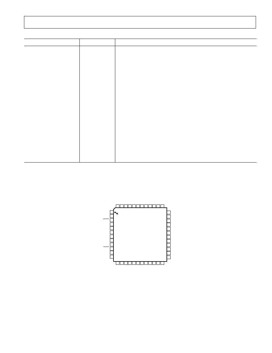
PIN FUNCTION DESCRIPTIONS
Pin No.
Mnemonic
Description
1, 12, 16, 27, 29, 32, 34, 45
GND
Ground
2
A
IN
A
Analog Input for Channel A
3
AINA
Analog Input for Channel A (Complementary)
4
DFS/GAIN
Data Format Select and Analog Input Gain Mode. (Low = offset binary out-
put available, 1 V p-p supported; high = two's complement output available,
1 V p-p supported; floating = offset binary output available, 2 V p-p supported;
Set to V
REF
= two's complement output available, 2 V p-p supported.)
5
REF
IN
A
Reference Voltage Input for Channel A
6
REF
OUT
Internal Reference Voltage
7
REF
IN
B
Reference Voltage Input for Channel B
8
S1
User Select #1 (Refer to Table I)
9
S2
User Select #2 (Refer to Table I)
10
AINB
Analog Input for Channel B (Complementary)
11
A
IN
B
Analog Input for Channel B
13, 30, 31, 48
V
D
Analog Supply (3 V)
14
ENC
B
Clock Input for Channel B
15, 28, 33, 46
V
DD
Digital Supply (2.5 V to 3.6 V)
1726
D9
B
D0
B
Digital Output for Channel B (D9
B
= MSB)
3544
D0
A
D9
A
Digital Output for Channel A (D9
A
= MSB)
47
ENC
A
Clock Input for Channel A
PIN CONFIGURATION
36
35
34
33
32
31
30
29
28
27
26
25
13 14 15 16 17 18 19 20 21 22 23 24
1
2
3
4
5
6
7
8
9
10
11
12
48 47 46 45 44
39 38 37
43 42 41 40
PIN 1
IDENTIFIER
TOP VIEW
(Not to Scale)
D1
A
D0
A
GND
V
DD
GND
V
D
V
D
GND
A
IN
A
A
IN
A
DFS/GAIN
REF
IN
A
REF
OUT
REF
IN
B
S1
S2
A
IN
B
A
IN
B
GND
V
DD
GND
D0
B
AD9218
GND
D1
B
V
D
ENC
A
V
DD
GND
D9
A
(MSB)
D8
A
D7
A
D6
A
D5
A
D4
A
D3
A
D2
A
V
D
ENC
B
V
DD
GND
(MSB) D9
B
D8
B
D7
B
D6
B
D5
B
D4
B
D3
B
D2
B

REV. 0
AD9218
8
TERMINOLOGY
Analog Bandwidth
The analog input frequency at which the spectral power of the
fundamental frequency (as determined by the FFT analysis) is
reduced by 3 dB.
Aperture Delay
The delay between the 50% point of the rising edge of the
ENCODE command and the instant at which the analog input
is sampled.
Aperture Uncertainty (Jitter)
The sample-to-sample variation in aperture delay.
Crosstalk
Coupling onto one channel being driven by a low level (40 dBFS)
signal when the adjacent interfering channel is driven by a
full-scale signal.
Differential Analog Input Resistance, Differential Analog
Input Capacitance and Differential Analog Input Impedance
The real and complex impedances measured at each analog
input port. The resistance is measured statically and the capaci-
tance and differential input impedances are measured with a
network analyzer.
Differential Analog Input Voltage Range
The peak-to-peak differential voltage that must be applied to
the converter to generate a full-scale response. Peak differential
voltage is computed by observing the voltage on a single pin
and subtracting the voltage from the other pin, which is 180
degrees out of phase. Peak-to-peak differential is computed by
rotating the inputs phase 180 degrees and again taking the peak
measurement. The difference is then computed between both
peak measurements.
Differential Nonlinearity
The deviation of any code width from an ideal 1 LSB step.
Effective Number of Bits
The effective number of bits (ENOB) is calculated from the
measured SNR based on the equation:
ENOB
SNR
dB
MEASURED
=
.
.
1 76
6 02
ENCODE Pulsewidth/Duty Cycle
Pulsewidth high is the minimum amount of time that the
ENCODE pulse should be left in Logic 1 state to achieve rated
performance; pulsewidth low is the minimum time ENCODE
pulse should be left in low state. See timing implications of
changing t
ENCH
in text. At a given clock rate, these specifica-
tions define an acceptable ENCODE duty cycle.
Full-Scale Input Power
Expressed in dBm. Computed using the following equation:
Power
V
Z
Full Scale
Full Scale rms
INPUT
-
-
=
10
0 001
2
log
.
Gain Error
Gain error is the difference between the measured and ideal full
scale input voltage range of the ADC.
Harmonic Distortion, Second
The ratio of the rms signal amplitude to the rms value of the
second harmonic component, reported in dBc.
Harmonic Distortion, Third
The ratio of the rms signal amplitude to the rms value of the
third harmonic component, reported in dBc.
Integral Nonlinearity
The deviation of the transfer function from a reference line
measured in fractions of 1 LSB using a "best straight line"
determined by a least square curve fit.
Minimum Conversion Rate
The encode rate at which the SNR of the lowest analog signal
frequency drops by no more than 3 dB below the guaranteed limit.
Maximum Conversion Rate
The encode rate at which parametric testing is performed.
Output Propagation Delay
The delay between a differential crossing of ENCODE and
ENCODE and the time when all output data bits are within
valid logic levels.
Noise (for Any Range within the ADC)
V
Z
NOISE
FS
SNR
Signal
dBm
dBc
dBFS
=
×
×
-
-
0 001 10
10
.
Where Z is the input impedance, FS is the full scale of the
device for the frequency in question, SNR is the value for the
particular input level, and Signal is the signal level within the
ADC reported in dB below full scale. This value includes both
thermal and quantization noise.
Power Supply Rejection Ratio
The ratio of a change in input offset voltage to a change in
power supply voltage.
Signal-to-Noise-and-Distortion (SINAD)
The ratio of the rms signal amplitude (set 1 dB below full scale)
to the rms value of the sum of all other spectral components,
including harmonics but excluding dc.
Signal-to-Noise Ratio (without Harmonics)
The ratio of the rms signal amplitude (set at 1 dB below full
scale) to the rms value of the sum of all other spectral compo-
nents, excluding the first five harmonics and dc.
Spurious-Free Dynamic Range (SFDR)
The ratio of the rms signal amplitude to the rms value of the
peak spurious spectral component. The peak spurious compo-
nent may or may not be a harmonic. May be reported in dBc
(i.e., degrades as signal level is lowered), or dBFS (always
related back to converter full scale).
Two-Tone Intermodulation Distortion Rejection
The ratio of the rms value of either input tone to the rms value
of the worst third order intermodulation product; reported in dBc.
Two-Tone SFDR
The ratio of the rms value of either input tone to the rms value
of the peak spurious component. The peak spurious component
may or may not be an IMD product. May be reported in dBc
(i.e., degrades as signal level is lowered), or in dBFS (always
related back to converter full scale).
REV. 0
AD9218
9
Worst Other Spur
The ratio of the rms signal amplitude to the rms value of the
worst spurious component (excluding the second and third
harmonic) reported in dBc.
Transient Response Time
Transient response is defined as the time it takes for the ADC to
reacquire the analog input after a transient from 10% above
negative full scale to 10% below positive full scale.
Out-of-Range Recovery Time
Out of range recovery time is the time it takes for the ADC to
reacquire the analog input after a transient from 10% above
positive full scale to 10% above negative full scale, or from 10%
below negative full scale to 10% below positive full scale.
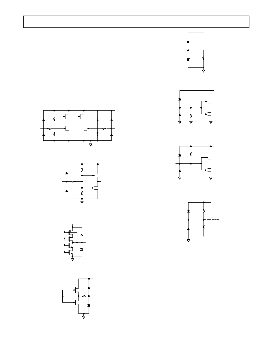
EQUIVALENT CIRCUITS
A
IN
40
40
30k
30k
15k
15k
V
D
A
IN
Figure 4. Analog Input Stage
ENCODE
2.6k
2.6k
600
V
D
Figure 5. Encode Inputs
OUT
V
D
Figure 6. Reference Output Stage
V
DD
40
DX
Figure 7. Digital Output Stage
REF
10k
V
D
Figure 8. Reference Inputs
S2
10k
V
D
Figure 9. S2 Input
S1
10k
V
D
Figure 10. S1 Input
DFS/GAIN
15k
15k
VREF
V
D
Figure 11. DFS/Gain Input
REV. 0
AD9218
10
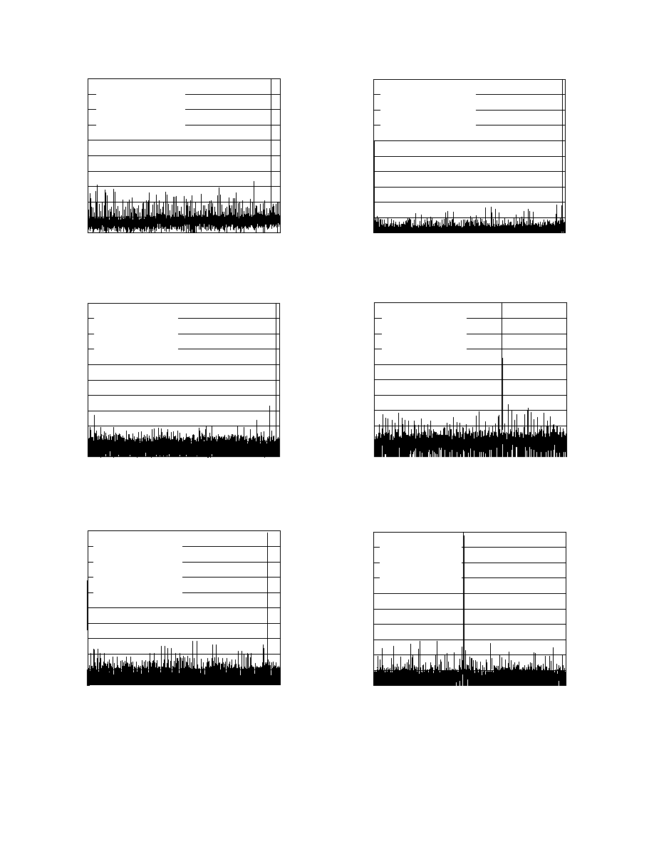
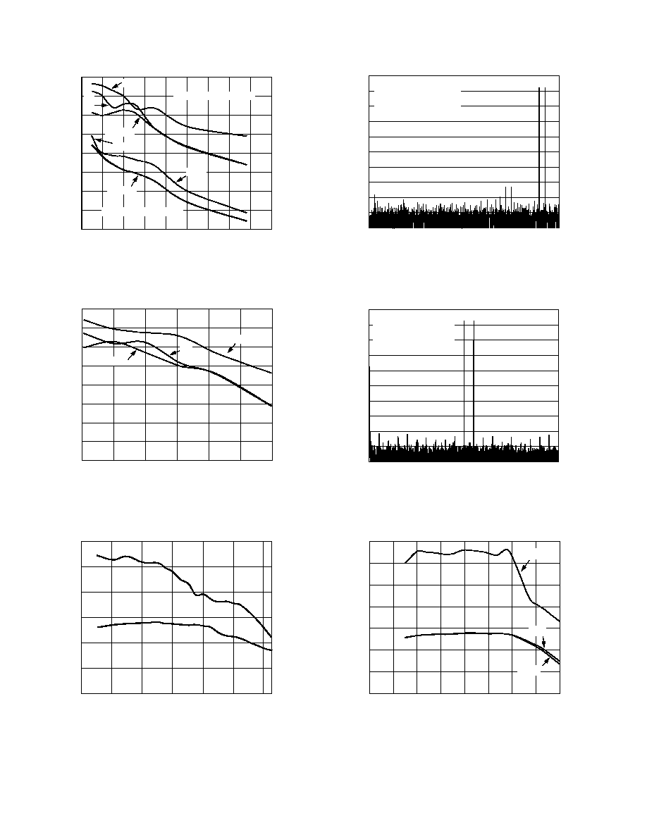
Typical Performance Characteristics
100
0
90
52.5
80
70
60
50
40
30
20
10
0
ENCODE = 105MSPS
A
IN
= 50.1MHz AT 0.5dBFS
SNR = 53.8dB
SINAD = 53.4dB
H2 = 69dB
H3 = 65.8dB
dB
TPC 1. FFT: FS = 105 MSPS, A
IN
= 50.1 MHz @ 0.5 dBFS,
Differential, 1 V p-p Input Range
0
10
20
30
40
50
60
70
80
90
100
dB
ENCODE = 80MSPS
A
IN
= 39MHz AT 0.5dBFS
SNR = 56.1dB
SINAD = 55.5dB
H2 = 71.8dB
H3 = 66.2dB
0
40
TPC 2. FFT: FS = 80 MSPS, A
IN
= 39 MHz @ 0.5 dBFS,
Differential, 1 V p-p Input Range
ENCODE = 65MSPS
A
IN
= 30.3MHz AT 0.5dBFS
SNR = 56.1dB
SINAD = 55.9dB
SFDR = 72dB
H2 = 83.2dB
H3 = 79dB
100
0
90
32.5
80
70
60
50
40
30
20
10
0
dB
TPC 3. FFT: FS = 65 MSPS, A
IN
= 30.3 MHz @ 0.5 dBFS,
Differential, 2 V p-p Input Range
0
10
20
30
40
50
60
70
80
90
100
dB
ENCODE = 40MSPS
A
IN
= 19.75 MHz AT 0.5dBFS
SNR = 58.4dB
SINAD = 58.3dB
H2 = 87dB
H3 = 81dB
0
20
TPC 4. FFT: FS = 40 MSPS, A
IN
= 19.7 MHz @ 0.5 dBFS,
Differential, 1 V p-p Input Range
100
0
90
40
80
70
60
50
40
30
20
10
0
ENCODE = 105MSPS
A
IN
= 70MHz AT 0.5dBFS
SNR = 51.9dB
SINAD = 51.8dB
H2 = 70.5dB
H3 = 76.3dB
dB
TPC 5. FFT: FS = 105 MSPS, A
IN
= 70 MHz @ 0.5 dBFS,
Differential, 1 V p-p Input Range
ENCODE = 65MSPS
A
IN
= 15MHz AT 0.5dBFS
SNR = 56.4dB
SINAD = 55.9dB
H2 = 73.9dB
H3 = 71.7dB
0
32.5
100
90
80
70
60
50
40
30
20
10
0
dB
TPC 6. FFT: FS = 65 MSPS, A
IN
= 15 MHz @ 0.5 dBFS;
with AD8138 Driving ADC Inputs, 1 V p-p Input Range
REV. 0
AD9218
11
0
10
20
30
40
50
60
70
80
90
100
dB
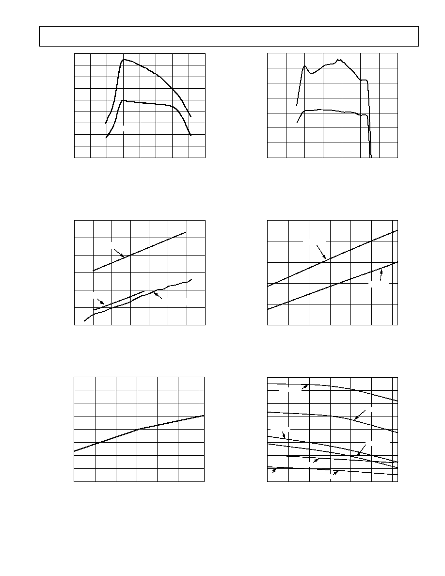
ENCODE = 31MSPS
A
IN
= 8MHz AT 0.5dBFS
SNR = 59.23dB
SINAD = 59.1dB
H2 = 87dB
H3 = 81dB
0
15.5
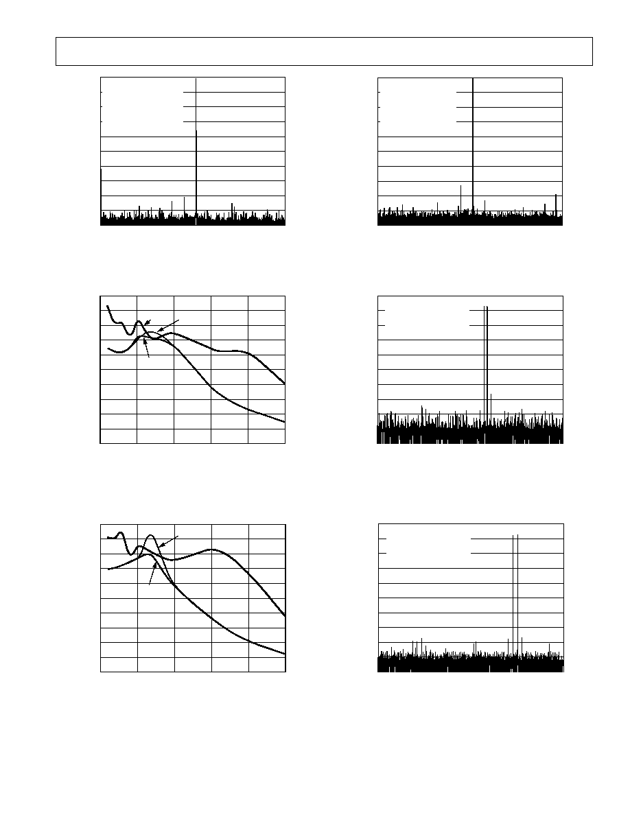
TPC 7. FFT: FS = 31 MSPS, A
IN
= 8 MHz @ 0.5 dBFS,
Differential, 1 V p-p Input Range
A
IN
FREQUENCY MHz
30
0
50
dB
2ND
3RD
SFDR
35
40
45
50
55
60
65
70
75
80
100
150
200
250
TPC 8. Harmonic Distortion (Second and Third) and SFDR
vs. A
IN
Frequency (1 V p-p, FS = 105 MSPS)
A
IN
FREQUENCY MHz
30
0
50
dB
2ND
3RD
SFDR
35
40
45
50
55
60
65
70
75
80
100
150
200
250
TPC 9. Harmonic Distortion (Second and Third) and SFDR
vs. A
IN
Frequency (1 V p-p, FS = 80 MSPS)
0
10
20
30
40
50
60
70
80
90
100
dB
ENCODE = 31MSPS
A
IN
= 8MHz AT 0.5dBFS
SNR = 59dB
SINAD = 58.8dB
H2 = 78.7dB
H3 = 72.9dB
0
15.5
TPC 10. FFT: FS = 31 MSPS, A
IN
= 8 MHz @ 0.5 dBFS;
with AD8138 Driving ADC Inputs, 1 V p-p Input Range
100
0
90
52.5
80
70
60
50
40
30
20
10
0
ENCODE = 105MSPS
A
IN
1 = 30.1MHz AT 7dBFS
A
IN
2 = 31.1MHz AT 7dBFS
SFDR = 67dBFS
dB
TPC 11. TwoTone Intermodulation Distortion (30 MHz
and 31 MHz; 1 V p-p, FS = 105 MSPS)
100
0
90
40
80
70
60
50
40
30
20
10
0
ENCODE = 80MSPS
A
IN
1 = 29.3MHz AT 7dBFS
A
IN
2 = 30.3MHz AT 7dBFS
SFDR = 77dBFS
dB
TPC 12. TwoTone Intermodulation Distortion (29.3 MHz,
30.3 MHz; 1 V p-p, FS = 80 MSPS)
REV. 0
AD9218
12
SFDR 1V
SFDR 2V
H3 2V
H2 2V
H3
1V
H2 1V
A
IN
FREQUENCY MHz
dB
0
20
40
60
80
100
120
140
160
180
10
20
30
40
60
70
80
90
50
2V SINGLE-ENDED DRIVE
1V DIFFERENTIAL DRIVE
TPC 13. Harmonic Distortion (Second and Third) and
SFDR vs. A
IN
Frequency (FS = 65 MSPS)
3rd
SFDR
A
IN
FREQUENCY MHz
dB
10
20
30
40
50
60
70
90
85
80
75
70
65
60
55
50
2nd
TPC 14. Harmonic Distortion (Second and Third) and
SFDR vs. A
IN
Frequency (1 V p-p, FS = 40 MSPS)
ENCODE RATE MSPS
0
20
dB
SINAD
SFDR
45
60
65
75
40
60
80
100
50
55
70
120
TPC 15. SINAD and SFDR vs. Encode Rate
(f
IN
= 10.3 MHz, 105 MSPS Grade) A
IN
= 0.5 dBFS
Differential, 1 V p-p Analog Input Range
100
0
90
32.5
80
70
60
50
40
30
20
10
0
ENCODE = 65MSPS
A
IN
1 = 28.1MHz AT 7dBFS
A
IN
2 = 29.1MHz AT 7dBFS
SFDR = 72.9dBFS
dB
TPC 16. Two-Tone Intermodulation Distortion
(28 MHz, 29 MHz; 1 V p-p, FS = 65 MSPS)
0
10
20
30
40
50
60
70
80
90
100
dB
ENCODE = 40MSPS
A
IN
1 = 10MHz AT 7dBFS
A
IN
2 = 11MHz AT 7dBFS
SFDR = 74dBc
0
20
TPC 17. TwoTone Intermodulation Distortion
(10 MHz, 11 MHz; 1 V p-p, FS = 40 MSPS)
ENCODE RATE MHz
dB
0
10
20
30
40
45
50
55
65
70
75
80
60
50
60
70
80
SINAD
SNR
SFDR
TPC 18. SINAD and SFDR vs. Encode Rate
(A
IN
= 10.3 MHz, 65 MSPS Grade) A
IN
= 0.5 dBFS
Differential, 1 V p-p Analog Input Range
REV. 0
AD9218
13
ENCODE POSITIVE PULSEWIDTH ns
30
0
1
dB
35
40
45
50
55
60
65
70
75
2
3
4
5
6
7
8
SFDR
SINAD
TPC 19. SINAD and SFDR vs. Encode Pulsewidth High.
A
IN
= 0.5 dBFS Single-Ended, 1 V p-p Analog Input
Range 105 MSPS
ENCODE CLOCK RATE MSPS
0
20
mA
140
200
180
160
120
100
80
40
60
80
100
120
140
50
45
40
35
30
25
20
15
10
5
0
IV
DD
mA
IV
D
-65
-65/-105 IV
DD
IV
D
-105
TPC 20. I
VD
and I
VDD
vs. Encode Rate (A
IN
= 10.3 MHz,
@ 0.5 dBFS). -65/-105 MSPS Grade Cl = 5 pF
TEMPERATURE C
V
1.231
1.229
1.227
1.225
1.223
1.221
1.119
40
20
0
20
40
60
80
TPC 21. V
REF
Output Voltage vs. Temperature
(I
LOAD
= 300
µA)
ENCODE POSITIVE PULSEWIDTH ns
75
70
65
60
55
50
45
40
0
4
6
8
10
12
2
14
dB
SINAD
SFDR
TPC 22. SINAD and SFDR vs. Encode Pulsewidth High.
A
IN
= 0.5 dBFS Single Ended, 1 V p-p Analog Input
Range 65 MSPS
TEMPERATURE C
4.5
4.0
3.5
3.0
2.5
2.0
40
20
0
20
40
60
80
GAIN -65
GAIN -105
%
TPC 23. Gain Error vs. Temperature. A
IN
= 10.3 MHz,
-65 MSPS Grade, -105 MSPS Grade, 1 V p-p
TEMPERATURE C
dB
68
66
64
62
60
58
56
54
52
40
20
0
20
40
60
80
SFDR -105
SFDR -65
SNR -65
SINAD -65
SNR -105
SINAD -105
TPC 24. SNR, SINAD, SFDR vs. Temperature.
A
IN
= 10.3 MHz , -65 MSPS Grade, -105 MSPS Grade,
1 V p-p
REV. 0
AD9218
14
I
LOAD
mA
1.50
1.45
1.40
1.35
1.30
1.25
1.20
1.15
1.10
1.0
0.5
0
0.5
1.0
1.5
2.0
1.05
1.00
V
2.5
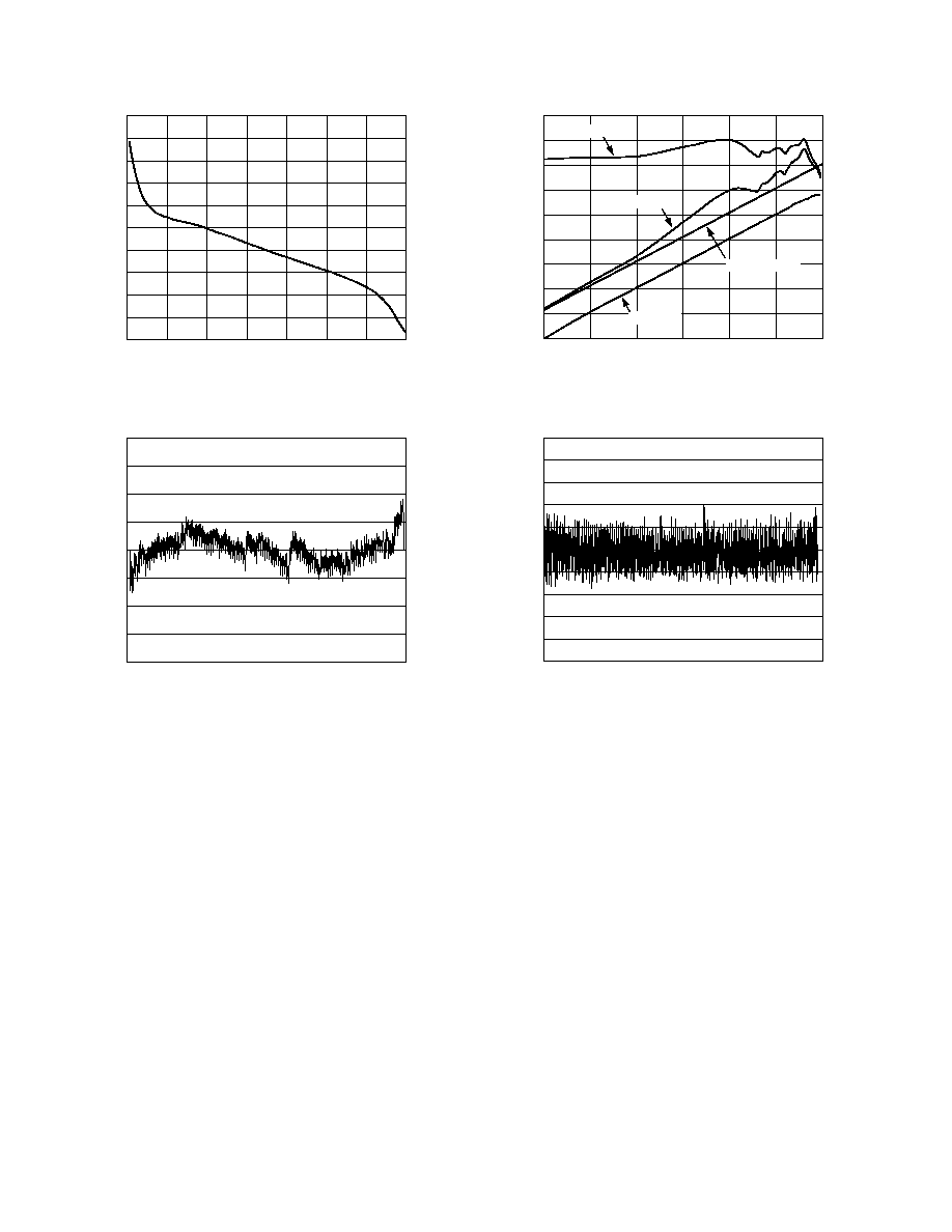
TPC 25. V
REF
vs. I
LOAD
2.0
1.5
1.0
0.5
0
0.5
1.0
1.5
2.0
LSB
0
1024
CODES
TPC 26. Typical INL Plot. 10.3 MHz A
IN
@ 80 MSPS
A
IN
INPUT LEVEL dBFS
90
80
70
60
50
40
30
20
10
0
60
50
40
30
20
10
0
dB
SFDR dBFS
SFDR dBc
70 dB REF LINE
SNR dBc
TPC 27. SFDR vs. A
IN
Input Level. 10.3 MHz A
IN
@ 80 MSPS
1.0
0.8
0.6
0.4
0
0.4
0.6
0.8
1.0
LSB
0
1024
CODES
0.2
0.2
TPC 28. Typical DNL Plot. 10.3 MHz A
IN
@ 80 MSPS
REV. 0
AD9218
15
THEORY OF OPERATION
The AD9218 ADC architecture is a bit-per-stage pipeline-type
converter utilizing switch capacitor techniques. These stages
determine the 7 MSBs and drive a 3-bit flash. Each stage provides
sufficient overlap and error correction allowing optimization of
comparator accuracy. The input buffers are differential, and both
sets of inputs are internally biased. This allows the most flexible
use of ac-coupled or dc-coupled and differential or single-ended
input modes. The output staging block aligns the data, carries
out the error correction, and feeds the data to output buffers.
The set of output buffers are powered from a separate supply,
allowing adjustment of the output voltage swing. There is no
discernible difference in performance between the two channels.
USING THE AD9218
ENCODE Input
Any high-speed A/D converter is extremely sensitive to the
quality of the sampling clock provided by the user. A Track/
Hold circuit is essentially a mixer. Any noise, distortion, or
timing jitter on the clock will be combined with the desired
signal at the A/D output. For that reason, considerable care has
been taken in the design of the ENCODE input of the AD9218,
and the user is advised to give commensurate thought to the clock
source. The ENCODE input is fully TTL/CMOS-compatible.
Digital Outputs
The digital outputs are TTL/CMOS-compatible for lower
power consumption. During power-down, the output buffers
transition to a high impedance state. A data format selection
option supports either two's complement (set high) or offset
binary output (set low) formats.
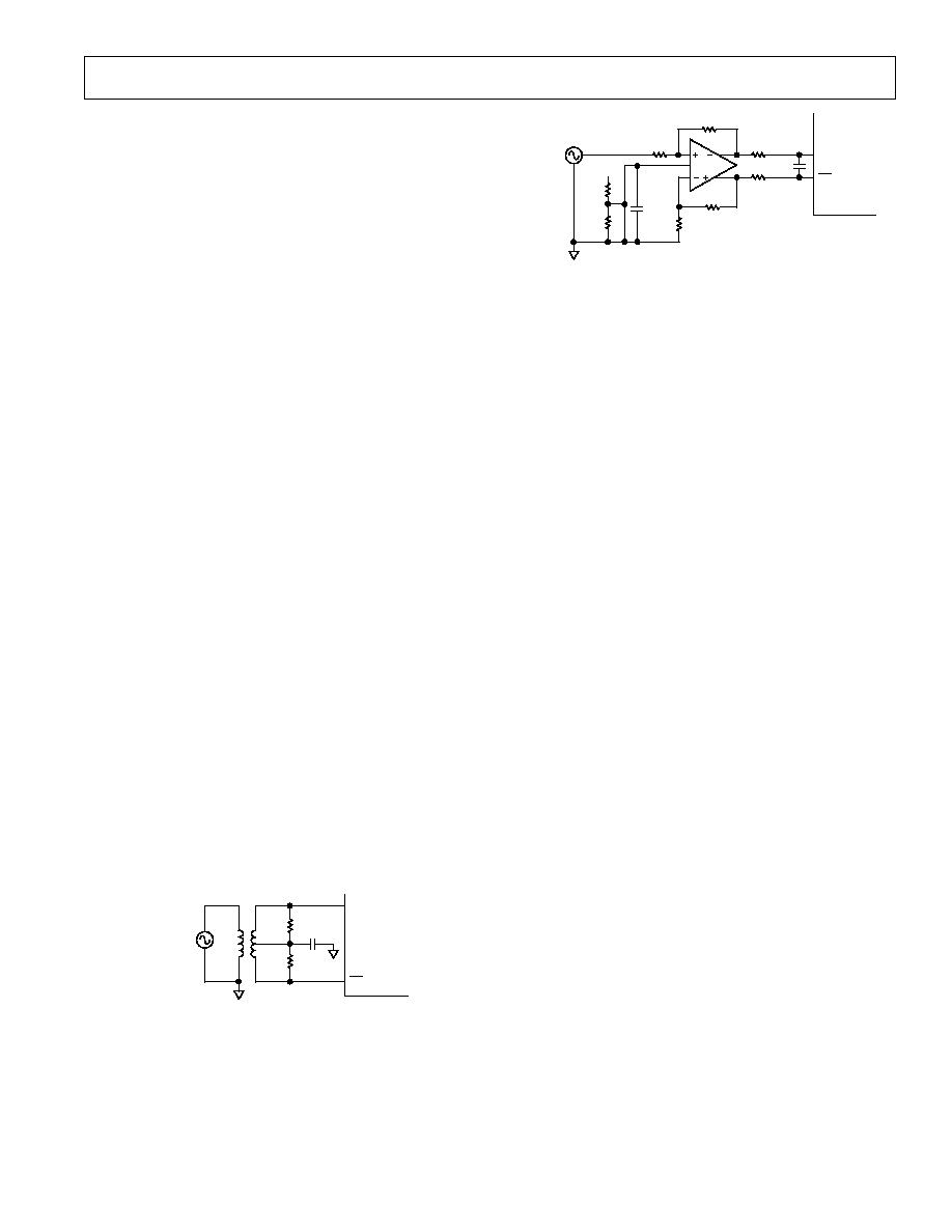
Analog Input
The analog input to the AD9218 is a differential buffer. For
best dynamic performance, impedance at AIN and
AIN should
match. Special care was taken in the design of the analog input
section of the AD9218 to prevent damage and corruption of
data when the input is overdriven. The nominal input range is
1.024 V p-p. Optimum performance is obtained when the part is
driven differentially where common mode noise is minimized
and even order harmonics are reduced. An example of driving
the AD9218 differentially via a wideband RF transformer for
ac-coupled applications is shown in Figure 12. Applications
that require dc-coupled differential drive can be accommo-
dated using the AD8138 differential output op amp, shown
in Figure 13.
25
25
0.1 F
1:1
A
IN
A
IN
AD9218
50
ANALOG
SIGNAL
SOURCE
Figure 12. Using a Wideband Transformer to Drive the
AD9218
10k
A
IN
A
IN
AD9218
50
ANALOG
SIGNAL
SOURCE
0.1 F
15pF
25
25
500
VOCM
500
500
525
5k
AV
DD
AD8138
Figure 13. Using the AD8138 to Drive the AD9218
Voltage Reference
A stable and accurate 1.25 V voltage reference is built into the
AD9218 (VREF OUT). In normal operation, the internal refer-
ence is used by strapping Pin 5 (REF
IN
A) and Pin 7 (REF
IN
B)
to Pin 6 (REF
OUT
). The input range for each channel can be
adjusted independently by varying the reference voltage inputs
applied to the AD9218. No appreciable degradation in per-
formance occurs when the reference is adjusted
± 5%. The
full-scale range of the ADC tracks reference voltage, which
changes linearly.
Timing
The AD9218 provides latched data outputs, with five pipeline
delays. Data outputs are available one propagation delay (t
PD
)
after the rising edge of the encode command (see Timing Dia-
gram). The length of the output data lines and loads placed
on them should be minimized to reduce transients within the
AD9218. These transients can detract from the converter's
dynamic performance.
The minimum guaranteed conversion rate of the AD9218 is
20 MSPS. At clock rates below 20 MSPS, dynamic performance
will degrade.
User Select Options
Two pins are available for a combination of operational modes.
These options allow the user to power-down both channels,
excluding the reference, or just the B channel. Both modes place
the output buffers in a high impedance state. Recovery from a
power-down state is accomplished in 10 clock cycles following
power-on.
The other option allows the user to skew the B Channel output
data by one-half a clock cycle. In other words, if two clocks are
fed to the AD9218 and are 180 degrees out of phase, enabling
the data align will allow Channel B output data to be available
at the rising edge of Clock A. If the same encode clock is pro-
vided to both channels and the data align pin is enabled, output
data from Channel B will be 180 degrees out of phase with
respect to Channel A. If the same encode clock is provided to
both channels and the data align pin is disabled, both outputs are
delivered on the same rising edge of the clock.
REV. 0
AD9218
16
APPLICATIONS
The wide analog bandwidth of the AD9218 makes it attractive
for a variety of high-performance receiver and encoder appli-
cations. Figure 14 shows the dual ADC in a typical low cost
I and Q demodulator implementation for cable, satellite, or
wireless LAN modem receivers. The excellent dynamic perfor-
mance of the ADC at higher analog input frequencies and
encode rates empowers users to employ direct IF sampling
techniques. IF sampling eliminates or simplifies analog mixer
and filter stages to reduce total system cost and power.
AD9218
IF IN
90
VCO
BPF
BPF
Q
ADC
I
ADC
VCO
Figure 14. Typical I/Q Demodulation Scheme
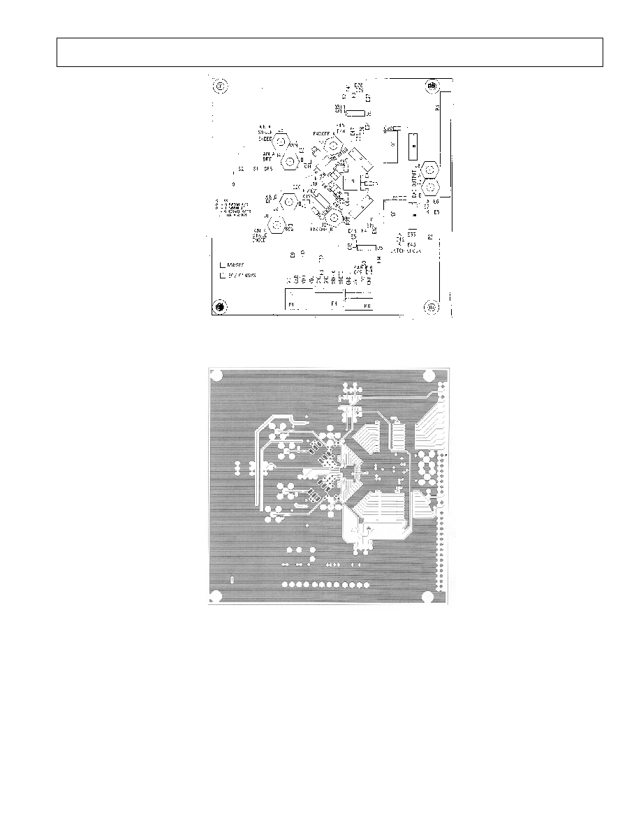
EVALUATION BOARD
The AD9218 evaluation board offers an easy way to test the
AD9218. It provides a means to drive the analog inputs single-
endedly or differentially. Differential drive can be tested through
a wideband RF transformer or a differential output operational
amplifier, the AD8138. The two encode clocks are accessible via
on-board SMB connectors J2, J7. These clocks are buffered
on board to provide the clocks for an on-board DAC and latches.
The digital outputs and output clocks are available at two 40-pin
connectors, P3 and P4. The board has several different modes
of operation, and is shipped in the following configuration:
· Differential Analog Input (RF Transformer Mode)
· Normal Operation Timing Mode
· Internal Voltage Reference
Power Connector
Power is supplied to the board via a detachable 12-pin power strip.
+5 V Optional Supply for Operational Amplifier
5 V Optional Supply for Operational Amplifier
V
REF
A Optional External Reference Input
V
REF
B Optional External Reference Input
V
DL
Supply for Support Logic and DAC
V
DD
Supply for ADC Outputs
V
D
Supply for ADC Analog
Analog Inputs
The evaluation board accepts a 1 V analog input signal centered
at ground at each analog input. SMB connectors J4 and J6 are
used for A
IN
and B
IN
respectively. These signals each drive a
wideband RF transformer T1, T2, allowing the ADC performance
for differential inputs to be measured using a single-ended source.
In this mode resistors R35, R33, R39, and R32 should not be in
place. Each analog input is terminated on the board with 50
to
ground. Each input is ac-coupled on the board through a 0.1
µF
capacitor to an on-chip resistor divider that provides dc bias.
Single-ended performance can be measured by bypassing the
transformers using connectors SMB J5 (Channel A) and J1
(Channel B). In this mode, place a 0
resistor at R35 and R33
(A Channel) and place R39 and R32 (B Channel). Note that the
inverting analog inputs are terminated on the board with 25
(optimized for differential operation). When driving the board
single-ended these resistors (R1, R3) can be changed to 50
to
provide balanced inputs. The operational amplifier can be
used by connecting to J5 (Channel A) and J1 (Channel B).
The ac-coupling capacitors on the top level should be removed
from the board to use the operational amplifier. The compo-
nents to use the op amp should be placed on the bottom of the
board. See PCB Bill of Materials list for values.
Encode
The encode clock for Channel A uses SMB connector J7.
Channel B encode uses SMB connector J2. Each clock input is
terminated on the board with 50
to ground. The input clocks
are fed directly to the ADC and to buffers U5, U6, which drive
the DAC and latches. The clock inputs are TTL-compatible.
Voltage Reference
The AD9218 has an internal 1.25 V voltage reference. An exter-
nal reference for each channel may be employed instead. The
evaluation board is configured for the internal reference (use
jumpers E18E1 and E17E19). To use external references,
connect to V
REF
A and V
REF
B pins on the power connector P1
and use jumpers E20E18 and E19E21.
Normal Operation Mode
In this mode both converters are clocked by the same encode
clock, latency is five clock cycles (see Timing Diagram). Signal
S1 (Pin 8) is held high and signal S2 (Pin 9) is held low. This is
set with the jumpers labeled S1 and S2 (near the analog input).
Data Align Mode
In this mode channel B output is delayed an additional one-half
cycle. Signals S1 (Pin 8) and signal S2 (Pin 9) are both held
high. This is set with the jumpers labeled S1 and S2 (near the
analog input).
Data Format Select
Data Format Select sets the output data format and the gain of
the ADC. Setting DFS (Pin 4) low sets the output format to be
offset binary and gain of 1; setting DFS high sets the output to
be two's complement and gain of 1. Removing the jumper for
DFS sets the output data format to offset binary and a gain of 2;
setting DFS to the middle selection sets the output data format
to two's complement and a gain of 2.
REV. 0
AD9218
17
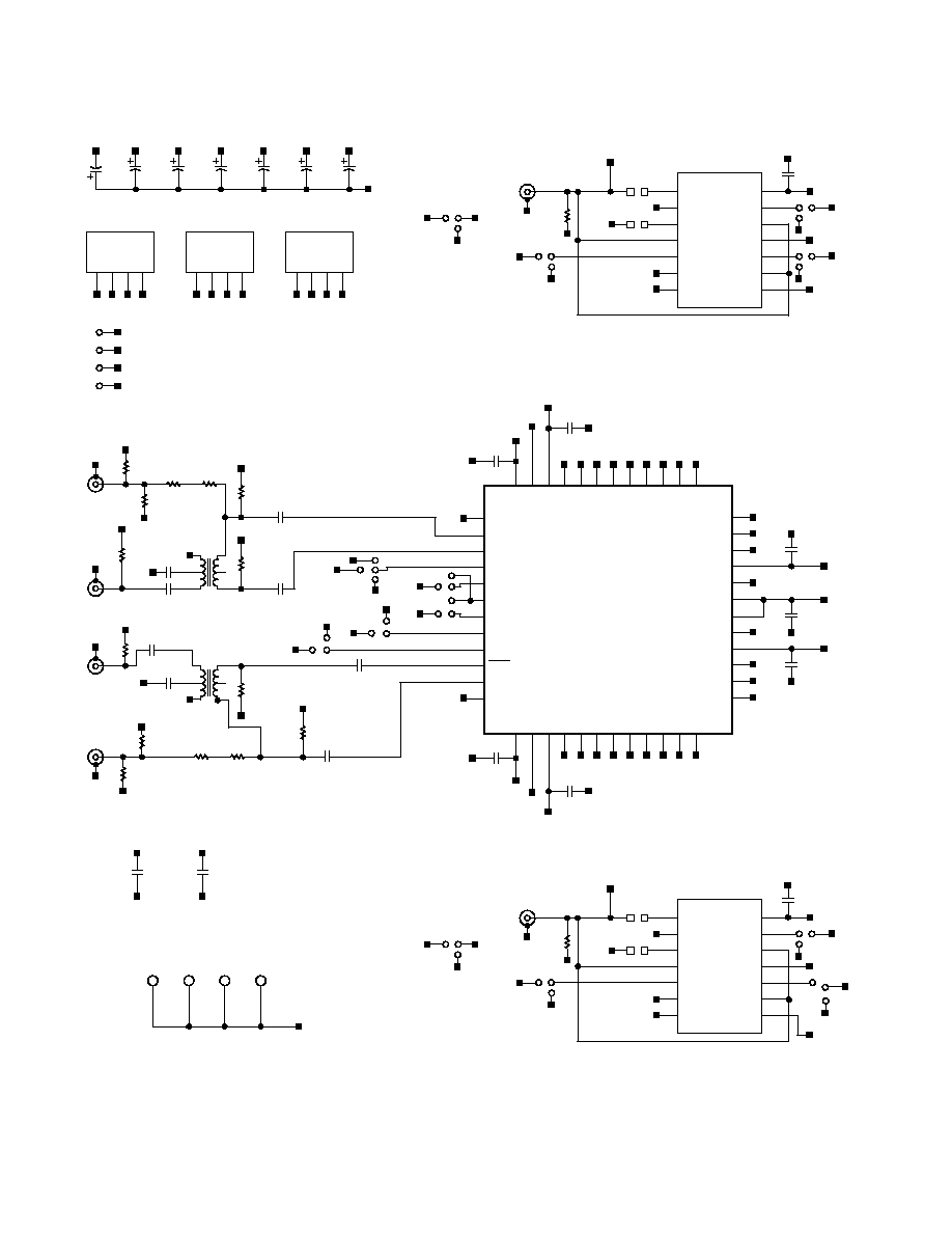
PCB Bill of Materials
#
Qty
REFDES
Device
Package
Value
1
29
C1, C3C15, C20C25, C27C35
Capacitor
0603
0.1
µF
2
2
C2, C36
Capacitor
0603
15 pF
3
7
C16, C17, C18, C19, C26, C37, C38
Capacitor
TAJD
10
µF
6
8
J1, J2, J3, J4, J5, J6, J7, J8
Connector
SMB
7
3
P1, P4, P11
4-Pin Power Connector
TB4
Wieland
25.531.3425.0
Z5.602.5453.0
8
2
P2, P3
HEADER40
10
8
R1R4, R22R24, R30
Resistor
0603
25
11
10
R5R12, R34, R37
Resistor
0603
50
12
2
R13, R14
Resistor
0603
2 k
13
6
R15, R17, R18, R26, R29, R31
Resistor
0603
500
14
2
R16, R25
Resistor
0603
525
15
2
R19, R27
Resistor
0603
4 k
16
8
R20, R32, R33, R35, R36, R38R40
Resistor
0603
0
17
2
R21, R28
Resistor
0603
1 k
18
2
T1, T2
Transformer
ADT-1-1WT
Minicircuits
19
1
U1
AD9218
LQFP48
20
2
U2, U3
74LCX821
SO24M3
21
1
U4
AD9763
LQFP48
22
2
U5, U6
74LCX86
SO14
23
4
U7, U8, U9, U10
Resistor Array
CTS20
22
24
2
U11, U12
AD8138
SO8NB
NOTE
R22, R23, R24, R30, R32, R33, R35, R36, R38, R39, R40, C2, C36 not placed on board.
Data Outputs
The ADC digital outputs are latched on the board by two
LCX821s, the latch outputs are available at the two 40-pin
connectors at Pins 2333 on P3 (Channel A) and Pins 2333 on
P4 (Channel B). The latch output clocks (data ready) are avail-
able at Pin 4 on P3 (Channel A) and Pin 4 on P4 (Channel B).
The data ready signal on Channel B can be aligned with Clock
A input by connecting E43E42 or aligned with Clock B input
by connecting E42E33.
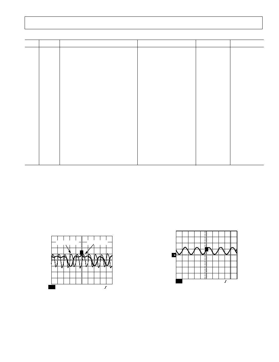
CH1
2.00V CH2 2.00V
M 10.0ns
CH4
40mV
PIN 31 (DATA)
PIN 37 (CLOCK)
T
Figure 15. Data Output and Clock at 80-Pin Connector
DAC Outputs
Each channel is reconstructed by an on-board dual channel DAC,
an AD9763. This DAC is intended to assist in debug only. It
should not be used to measure the performance of the ADC.
It is a current output DAC with on-board 50
termination
resistors. Figure 16 is representative of the DAC output with a
full-scale analog input. The scope setting was low bandwidth,
50
termination.
CH1
500mV
M 50.0ns
CH1
380mV
1
T
Figure 16. DAC Output
REV. 0
AD9218
18
1A
1B
1Y
2A
2B
2Y
GND
1
2
3
4
5
6
7
14
13
12
11
10
9
8
V
CC
4B
4A
4Y
3B
3A
3Y
U5
74LCX86
GND
C13
0.1 F
V
DL
V
DL
V
DL
CLKLATB
E5
E44
E4
GND
E15
E11
E12
GND
CLKDACB
P23
TIEB
P22
ENC
B
P20 P21
ENC
B
E13
E16
E14
J2
ENCODE B
GND
GND
R7
50
E49
E48
E50
GND
V
DL
GND
V
DL
TIEB
GND
DRB
DUT CLOCK SELECTABLE TO BE DIRECT OR BUFFERED
1A
1B
1Y
2A
2B
2Y
GND
1
2
3
4
5
6
7
14
13
12
11
10
9
8
V
CC
4B
4A
4Y
3B
3A
3Y
U8
74LCX86
GND
C25
0.1 F
V
DL
V
DL
V
DL
CLKDACA
E40
E41
E3
GND
E39 E38
E37
GND
DRA
P13
TIEA
P14
ENC
A
P12 P19
ENC
A
E35
E36
E34
J7
ENCODE A
GND
GND
R11
50
E46
E45
E47
GND
V
DL
GND
V
DL
TIEA
GND
CLKLATA
DUT CLOCK SELECTABLE TO BE DIRECT OR BUFFERED
GND
1
2
3
4
5
6
7
8
9
10
11
12
36
35
34
33
32
31
30
29
28
27
26
25
48
47
46
45
44
43
42
41
40
39
38
37
13
14
15
16
17
18
19
20
21
22
23
24
AD9218
U1
GND
A
IN
A
A
IN
AB
DFS/GAIN
REF
IN
A
REF
OUT
REF
IN
B
S1
S2
A
IN
B
A
IN
B
GND
V
D
ENC
A
V
DD
GND
D9A
D8A
D7A
D6A
D5A
D4A
D3A
D2A
V
D
ENC
B
V
DD
GND
D9B
D8B
D7B
D6B
D5B
D4B
D3B
D2B
D1A
D0A
GND
V
DD
GND
V
D
V
D
GND
V
DD
GND
D0B
D1B
E1
E18
E20
E17
VREFA
VREFB
E19
E21
E30
A
IN
AB
GND
A
IN
A
REF
OUT
E2
E27
E25
GND
GND
E29
E22
E28
E26
GND
V
D
GND
GND
6
5
4
GND
1
2
3
C31
0.1 F
6
5
4
GND
1
2
3
C30
0.1 F
GND
GND
C10
0.1 F
C9
0.1 F
C12
0.1 F
R1
25
R2
25
R4
25
C11
0.1 F
R3
25
R32
0
R39
0
GND
GND
J5
A
IN
A
SINGLE-ENDED
GND
J4
A
IN
A
DIFFERENTIAL
GND
J6
A
IN
B
DIFFERENTIAL
GND
J1
A
IN
B
SINGLE-ENDED
GND
C37
10 F
5V
C38
10 F
V
D
C16
10 F
V
DD
C17
10 F
V
DL
C18
10 F
VREFA
C19
10 F
C26
10 F
VREFB
+5V
4
GND
3
+5V
2
5V
1
GND
P11
P4
P1
4
GND
3
GND
2
VREFA
1
VREFB
4
V
D
3
V
DD
2
1
GND
V
DL
GND
D0B
D1B
C1
0.1 F
V
DD
GND
C3
0.1 F
GND
GND
GND
V
D
GND
D1A
D0A
GND
C4
0.1 F
V
DD
GND
GND
D9A
D8A
D7A
D6A
D5A
D4A
D3A
D2A
GND
C8
0.1 F
GND
C7
0.1 F
V
D
ENC
A
V
DD
GND
C5
0.1 F
GND
C6
0.1 F
V
D
ENC
B
V
DD
GND
D9B
D8B
D7B
D6B
D5B
D4B
D3B
D2B
C24
0.1 F
GND
REF
IN
B
C27
0.1 F
GND
REF
IN
A
H3
MT HOLE6
GND
H1
MT HOLE6
H2
MT HOLE6
H4
MT HOLE6
E9
V
D
E10
V
DD
E32
V
DD
E31
V
DL
OPTIONAL INPUT PATH FOR OPAMP OR SINGLE-ENDED
OPTIONAL INPUT PATH FOR OPAMP OR SINGLE-ENDED
A
IN
B
A
IN
BB
V
D
V
D
E23
E24
C15
0.1 F
GND
R6
50
C14
0.1 F
GND
R5
50
T2
R33
00
R35
00
AMP
IN
A
R36
0
GND
R34
50
AMP
IN
B
R38
0
GND
R37
50
T1
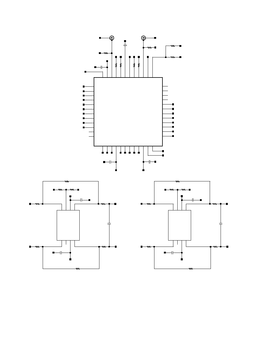
Figure 17a. PCB Schematic
REV. 0
AD9218
19
1
2
3
4
5
6
7
8
9
10
1
2
3
4
5
6
7
8
9
10
20
19
18
17
16
15
14
13
12
11
20
19
18
17
16
15
14
13
12
11
CT520
VALUE = 22
GND
C21
0.1
F
D9A
D8A
D7A
D6A
D5A
D4A
D3A
D2A
D1A
D0A
D9M
D8M
D7M
D6M
D5M
D4M
D3M
D2M
D1M
D0M
GND
X0
X1
X2
X3
X4
X5
X6
X7
X8
X9
GND
1
2
3
4
5
6
7
8
9
10
11
12
24
23
22
21
20
19
18
17
16
15
14
13
V
CC
Y0
Y1
Y2
Y3
Y4
Y5
Y6
Y7
Y8
Y9
CLK
74LCX821
GND
D9M
D8M
D7M
D6M
D5M
D4M
D3M
D2M
D1M
D0M
GND
V
DL
D9X
D8X
D7X
D6X
D5X
D4X
D3X
D2X
D1X
D0X
CLKLATA
U2
1
2
3
4
5
6
7
8
9
10
1
2
3
4
5
6
7
8
9
10
20
19
18
17
16
15
14
13
12
11
20
19
18
17
16
15
14
13
12
11
CT520
VALUE = 22
D9X
D8X
D7X
D6X
D5X
D4X
D3X
D2X
D1X
D0X
D9P
D8P
D7P
D6P
D5P
D4P
D3P
D2P
D1P
D0P
40
38
36
34
32
30
28
26
24
22
20
18
16
14
12
10
8
6
4
2
39
37
35
33
31
29
27
25
23
21
19
17
15
13
11
9
7
5
3
1
HEADER40
GND
DRA
GND
D9P
D8P
D7P
D6P
D5P
D4P
D3P
D2P
D1P
D0P
GND
GND
GND
GND
GND
GND
GND
P3
GND
39
37
35
33
31
29
27
25
23
21
19
17
15
13
11
9
7
5
3
1
40
38
36
34
32
30
28
26
24
22
20
18
16
14
12
10
8
6
4
2
U7
U9
1
2
3
4
5
6
7
8
9
10
1
2
3
4
5
6
7
8
9
10
20
19
18
17
16
15
14
13
12
11
20
19
18
17
16
15
14
13
12
11
CT520
VALUE = 22
E7
E6
E8
DRB
GND
C20
0.1
F
D0B
D1B
D2B
D3B
D4B
D5B
D6B
D7B
D8B
D9B
D0N
D1N
D2N
D3N
D4N
D5N
D6N
D7N
D8N
D9N
OE
X0
X1
X2
X3
X4
X5
X6
X7
X8
X9
GND
1
2
3
4
5
6
7
8
9
10
11
12
24
23
22
21
20
19
18
17
16
15
14
13
V
CC
Y0
Y1
Y2
Y3
Y4
Y5
Y6
Y7
Y8
Y9
CLK
74LCX821
GND
D0N
D1N
D2N
D3N
D4N
D5N
D6N
D7N
D8N
D9N
GND
V
DL
D0Y
D0Y
D0Y
D0Y
D0Y
D0Y
D0Y
D0Y
D0Y
D0Y
U3
1
2
3
4
5
6
7
8
9
10
1
2
3
4
5
6
7
8
9
10
20
19
18
17
16
15
14
13
12
11
20
19
18
17
16
15
14
13
12
11
CT520
VALUE = 22
D0Y
D1Y
D2Y
D3Y
D4Y
D5Y
D6Y
D7Y
D8Y
D9Y
D0Q
D1Q
D2Q
D3Q
D4Q
D5Q
D6Q
D7Q
D8Q
D9Q
40
38
36
34
32
30
28
26
24
22
20
18
16
14
12
10
8
6
4
2
39
37
35
33
31
29
27
25
23
21
19
17
15
13
11
9
7
5
3
1
HEADER40
GND
GND
D9Q
D8Q
D7Q
D6Q
D5Q
D4Q
D3Q
D2Q
D1Q
D0Q
GND
GND
GND
GND
GND
GND
GND
P2
DRA
GND
39
37
35
33
31
29
27
25
23
21
19
17
15
13
11
9
7
5
3
1
40
38
36
34
32
30
28
26
24
22
20
18
16
14
12
10
8
6
4
2
E42
E33
E43
CLKLATA
CLKLATD
U8
U10
Figure 17b. PCB Schematic
REV. 0
AD9218
20
1
2
3
4
5
6
7
8
9
10
11
12
36
35
34
33
32
31
30
29
28
27
26
25
48
47
46
45
44
43
42
41
40
39
38
37
13
14
15
16
17
18
19
20
21
22
23
24
9763
DB8P1
DB7P1
DB6P1
DB5P1
DB4P1
DB3P1
DB2P1
DB1P1
DB0P1
NC
NC1
MODE
AV
DD
IA2
IB1
FSADJ1
REFIO
REFLO
FSADJ2
IB2IA2
ACOM
SLEEP
NC2
NC3
GND
DCOM1
DV
DD
WRT1/IQWRT
CLK1/IQCLK
CLK2/IQRESET
WRT2/IQSEL
DCOM2
DB9
P2
NC7
NC6
NC5
NC4
DB0P2
DB1P2
DB2P2
DB3P2
DB4P2
DB5P2
DB6P2
DB7P2
D0Y
C23
0.1 F
V
DL
C22
0.1 F
GND
C28
0.1 F
D1Y
D2Y
D3Y
D4Y
D5Y
D6Y
D7Y
D8Y
D9Y
D0X
D1X
D2X
D3X
D4X
D5X
D6X
D7X
GND
V
DL
GND
R10
50
J3
GND
GND
R12, 50
GND
R13, 2k
GND
GND
R14, 2k
GND
R8, 50
GND
GND
R9
50
GND
J8
DAC OUTPUT A
DAC OUTPUT B
GND
V
DL
GND
C29
0.1 F
D8X
D9X
V
DL
GND
GND
GND
CLKDACB
CLKDACB
CLKDACA
CLKDACA
GND
U4
NC = NO CONNECT
DB8
P2
DB9
P1
GND
R20
00
V
DL
R40
00
POWER-DOWN OPTION
AD8138
IN
VOCM
V+
+OUT
+IN
NC
V
OUT
1
2
3
4
8
7
6
5
R19
4k
R21
1k
+5V
C32
0.1 F
GND
R22
25
R23
25
C2
15pF
U11
5V
C33
0.1 F
AMP
IN
A
GND
R17
500
R16
525
GND
A
IN
A
AI
IN
AB
GND
5V
R15
500
R18
500
NC = NO CONNECT
AD8138
IN
VOCM
V+
+OUT
+IN
NC
V
OUT
1
2
3
4
8
7
6
5
R27
4k
R28
1k
+5V
C35
0.1 F
GND
R30
25
R24
25
C36
15pF
U12
5V
C34
0.1 F
AMP
IN
B
GND
R29
500
R25
525
GND
A
IN
BB
A
IN
B
GND
5V
R31
500
R26
500
NC = NO CONNECT
(OPTIONAL)
Figure 17c. PCB Schematic
REV. 0
AD9218
21
Figure 18. PCB Top Side Silkscreen
Figure 19. PCB Top Side Copper
REV. 0
AD9218
22
Figure 20. PCB Ground Layer
Figure 21. PCB Split Power Plane
REV. 0
AD9218
23
Figure 22. PCB Bottom Side Copper
Figure 23. Bottom Side Silkscreen
REV. 0
24
C020011.57/01(0)
PRINTED IN U.S.A.
AD9218
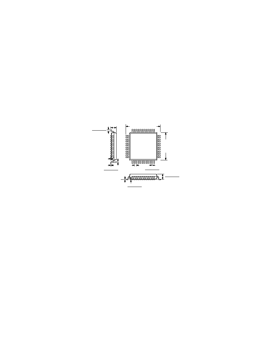
48-Lead LQFP
(ST-48)
TOP VIEW
(PINS DOWN)
1
12
13
25
24
36
37
48
0.019 (0.5)
BSC
0.276
(7.00)
BSC
SQ
0.011 (0.27)
0.006 (0.17)
0.354 (9.00) BSC SQ
0.063 (1.60)
MAX
0.030 (0.75)
0.018 (0.45)
0.008 (0.2)
0.004 (0.09)
0
MIN
COPLANARITY
0.003 (0.08)
SEATING
PLANE
0.006 (0.15)
0.002 (0.05)
7
0
0.057 (1.45)
0.053 (1.35)
OUTLINE DIMENSIONS
Dimensions shown in inches and (mm).
Troubleshooting
If the board does not seem to be working correctly, try the
following:
· Verify power at IC pins.
· Check that all jumpers are in the correct position for the
desired mode of operation.
· Verify V
REF
is at 1.23 V.
· Try running encode clock and analog inputs at low speeds
(20 MSPS/1 MHz) and monitor LCX821 outputs, DAC
outputs, and ADC outputs for toggling.
The AD9218 Evaluation Board is provided as a design example
for customers of Analog Devices, Inc. ADI makes no warranties,
express, statutory, or implied, regarding merchantability or
fitness for a particular purpose.
Document Outline
- Specifications
- Pinout
- Package drawings
- Ordering Guide
- Features
- Applications
- Product Description
- Absolute Maximum Ratings
- Functional Block Diagram
- Circuit Description
- Typical Characteristics
- PRODUCT HIGHLIGHTS
- EXPLANATION OF TEST LEVELS
- EQUIVALENT CIRCUITS
- USING THE AD9218
- APPLICATIONS
- EVALUATION BOARD
- DIAGRAMS
- Normal Operation, Same Clock (S1 = 1, S2 = 0) Channel Timing
- Normal Operation with Two Clock Sources (S1 = 1, S2 = 0) Channel Timing
- Data Align with Two Clock Sources (S1 = 1, S2 = 1) Channel Timing
- Analog Input Stage
- Encode Inputs
- Reference Output Stage
- Digital Output Stage
- Reference Inputs
- S2 Input
- S1 Input
- DFS/Gain Input
- Using a Wideband Transformer to Drive the AD9218
- Using the AD8138 to Drive the AD9218
- Typical I/Q Demodulation Scheme
- PCB Schematic 1
- PCB Schematic 2
- PCB Schematic 3
- PCB Top Side Silkscreen
- PCB Top Side Copper
- PCB Ground Layer
- PCB Split Power Plane
- PCB Bottom Side Copper
- Bottom Side Silkscreen