 | –≠–ª–µ–∫—Ç—Ä–æ–Ω–Ω—ã–π –∫–æ–º–ø–æ–Ω–µ–Ω—Ç: AD9280 | –°–∫–∞—á–∞—Ç—å:  PDF PDF  ZIP ZIP |
AD9280
One Technology Way, P.O. Box 9106, Norwood, MA 02062-9106, U.S.A.
Tel: 781/329-4700
World Wide Web Site: http://www.analog.com
Fax: 781/326-8703
© Analog Devices, Inc., 1999
REV. D
Information furnished by Analog Devices is believed to be accurate and
reliable. However, no responsibility is assumed by Analog Devices for its
use, nor for any infringements of patents or other rights of third parties
which may result from its use. No license is granted by implication or
otherwise under any patent or patent rights of Analog Devices.
a
Complete 8-Bit, 32 MSPS, 95 mW
CMOS A/D Converter
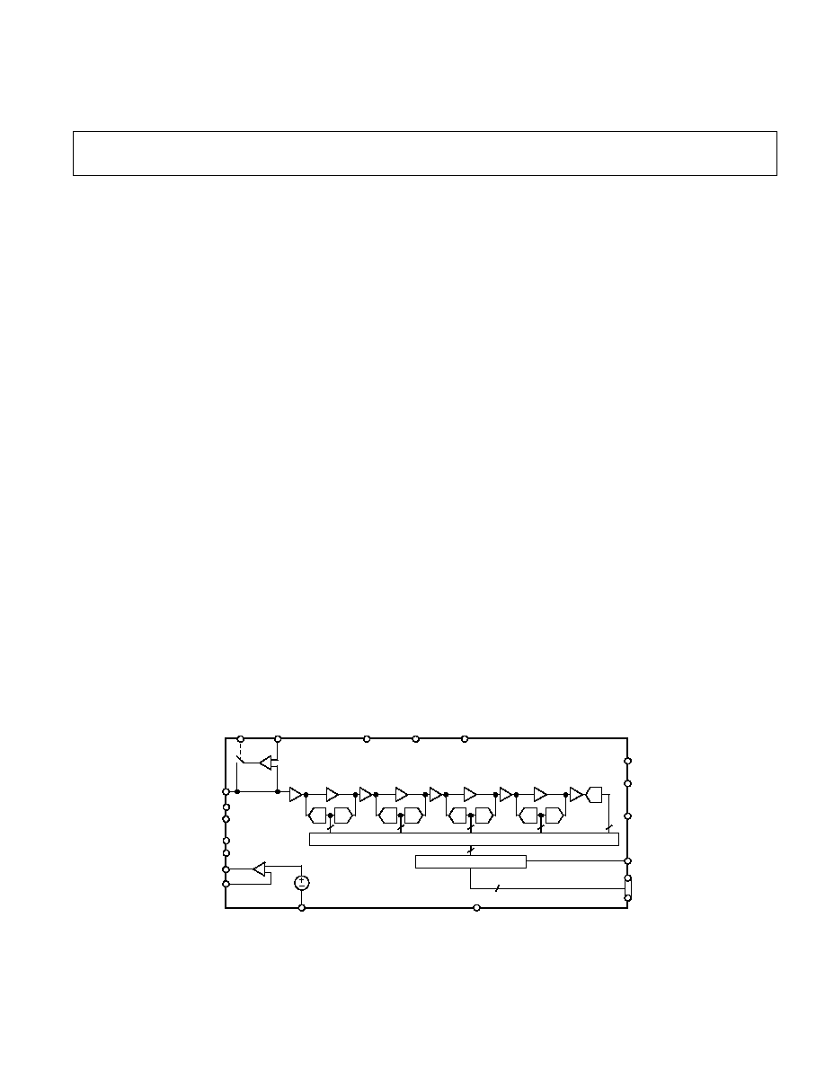
FUNCTIONAL BLOCK DIAGRAM
A/D
A/D
VINA
REFTF
REFBF
REFSENSE
OTR
D7 (MSB)
D0 (LSB)
VREF
DRVDD
AVDD
CLK
DRVSS
AD9280
SHA
SHA
SHA
GAIN
SHA
GAIN
GAIN
D/A
A/D
D/A
A/D
D/A
CORRECTION LOGIC
OUTPUT BUFFERS
REFTS
1V
AVSS
REFBS
THREE-
STATE
MODE
STBY
CLAMP
CLAMP
IN
SHA
GAIN
A/D
D/A
FEATURES
CMOS 8-Bit 32 MSPS Sampling A/D Converter
Pin-Compatible with AD876-8
Power Dissipation: 95 mW (3 V Supply)
Operation Between +2.7 V and +5.5 V Supply
Differential Nonlinearity: 0.2 LSB
Power-Down (Sleep) Mode
Three-State Outputs
Out-of-Range Indicator
Built-In Clamp Function (DC Restore)
Adjustable On-Chip Voltage Reference
IF Undersampling to 135 MHz
PRODUCT DESCRIPTION
The AD9280 is a monolithic, single supply, 8-bit, 32 MSPS
analog-to-digital converter with an on-chip sample-and-hold
amplifier and voltage reference. The AD9280 uses a multistage
differential pipeline architecture at 32 MSPS data rates and
guarantees no missing codes over the full operating temperature
range.
The input of the AD9280 has been designed to ease the devel-
opment of both imaging and communications systems. The user
can select a variety of input ranges and offsets and can drive the
input either single-ended or differentially.
The sample-and-hold amplifier (SHA) is equally suited for both
multiplexed systems that switch full-scale voltage levels in suc-
cessive channels and sampling single-channel inputs at frequen-
cies up to and beyond the Nyquist rate. AC-coupled input
signals can be shifted to a predetermined level, with an onboard
clamp circuit. The dynamic performance is excellent.
The AD9280 has an onboard programmable reference. An
external reference can also be chosen to suit the dc accuracy and
temperature drift requirements of the application.
A single clock input is used to control all internal conversion
cycles. The digital output data is presented in straight binary
output format. An out-of-range signal (OTR) indicates an over-
flow condition which can be used with the most significant bit
to determine low or high overflow.
The AD9280 can operate with a supply range from +2.7 V to
+5.5 V, ideally suiting it for low power operation in high speed
applications.
The AD9280 is specified over the industrial (≠40
∞
C to +85
∞
C)
temperature range.
PRODUCT HIGHLIGHTS
Low Power
The AD9280 consumes 95 mW on a 3 V supply (excluding the
reference power). In sleep mode, power is reduced to below
5 mW.
Very Small Package
The AD9280 is available in a 28-lead SSOP package.
Pin Compatible with AD876-8
The AD9280 is pin compatible with the AD876-8, allowing
older designs to migrate to lower supply voltages.
300 MHz Onboard Sample-and-Hold
The versatile SHA input can be configured for either single-
ended or differential inputs.
Out-of-Range Indicator
The OTR output bit indicates when the input signal is beyond
the AD9280's input range.
Built-In Clamp Function
Allows dc restoration of video signals.

≠2≠
REV. D
AD9280≠SPECIFICATIONS
(AVDD = +3 V, DRVDD = +3 V, F
S
= 32 MHz (50% Duty Cycle), MODE = AVDD, 2 V Input
Span from 0.5 V to 2.5 V, External Reference, T
MIN
to T
MAX
unless otherwise noted)
Parameter
Symbol
Min
Typ
Max
Units
Condition
RESOLUTION
8
Bits
CONVERSION RATE
F
S
32
MHz
DC ACCURACY
Differential Nonlinearity
DNL
±
0.2
±
1.0
LSB
REFTS = 2.5 V, REFBS = 0.5 V
Integral Nonlinearity
INL
±
0.3
±
1.5
LSB
Offset Error
E
ZS
±
0.2
±
1.8
% FSR
Gain Error
E
FS
±
1.2
±
3.9
% FSR
REFERENCE VOLTAGES
Top Reference Voltage
REFTS
1
AVDD
V
Bottom Reference Voltage
REFBS
GND
AVDD ≠ 1 V
Differential Reference Voltage
2
V p-p
Reference Input Resistance
1
10
k
REFTS, REFBS: MODE = AVDD
4.2
k
Between REFTF & REFBF: MODE = AVSS
ANALOG INPUT
Input Voltage Range
AIN
REFBS
REFTS
V
REFBS Min = GND: REFTS Max = AVDD
Input Capacitance
C
IN
1
pF
Switched
Aperture Delay
t
AP
4
ns
Aperture Uncertainty (Jitter)
t
AJ
2
ps
Input Bandwidth (≠3 dB)
BW
Full Power (0 dB)
300
MHz
DC Leakage Current
43
µ
A
Input =
±
FS
INTERNAL REFERENCE
Output Voltage (1 V Mode)
VREF
1
V
REFSENSE = VREF
Output Voltage Tolerance (1 V Mode)
±
10
±
25
mV
Output Voltage (2 V Mode)
VREF
2
V
REFSENSE = GND
Load Regulation (1 V Mode)
0.5
2
mV
1 mA Load Current
POWER SUPPLY
Operating Voltage
AVDD
2.7
3
5.5
V
DRVDD
2.7
3
5.5
V
Supply Current
IAVDD
31.7
36.7
mA
AVDD = 3 V, MODE = AVSS
Power Consumption
P
D
95
110
mW
AVDD = DRVDD = 3 V, MODE = AVSS
Power-Down
4
mW
STBY = AVDD, MODE and CLOCK
= AVSS
Gain Error Power Supply Rejection
PSRR
1
% FS
DYNAMIC PERFORMANCE (AIN = 0.5 dBFS)
Signal-to-Noise and Distortion
SINAD
f = 3.58 MHz
46.4
49
dB
f = 16 MHz
48
dB
Effective Bits
f = 3.58 MHz
7.8
Bits
f = 16 MHz
7.7
Bits
Signal-to-Noise
SNR
f = 3.58 MHz
47.8
49
dB
f = 16 MHz
48
dB
Total Harmonic Distortion
THD
f = 3.58 MHz
≠62
≠49.5
dB
f = 16 MHz
≠58
dB
Spurious Free Dynamic Range
SFDR
f = 3.58 MHz
66
51.4
dB
f = 16 MHz
61
dB
Differential Phase
DP
0.2
Degree
NTSC 40 IRE Mod Ramp
Differential Gain
DG
0.08
%

Parameter
Symbol
Min
Typ
Max
Units
Condition
DIGITAL INPUTS
High Input Voltage
V
IH
2.4
V
Low Input Voltage
V
IL
0.3
V
DIGITAL OUTPUTS
High-Z Leakage
I
OZ
≠10
+10
µ
A
Output = GND to VDD
Data Valid Delay
t
OD
25
ns
C
L
= 20 pF
Data Enable Delay
t
DEN
25
ns
Data High-Z Delay
t
DHZ
13
ns
LOGIC OUTPUT (with DRVDD = 3 V)
High Level Output Voltage (I
OH
= 50
µ
A)
V
OH
+2.95
V
High Level Output Voltage (I
OH
= 0.5 mA)
V
OH
+2.80
V
Low Level Output Voltage (I
OL
= 1.6 mA)
V
OL
+0.4
V
Low Level Output Voltage (I
OL
= 50
µ
A)
V
OL
+0.05
V
LOGIC OUTPUT (with DRVDD = 5 V)
High Level Output Voltage (I
OH
= 50
µ
A)
V
OH
+4.5
V
High Level Output Voltage (I
OH
= 0.5 mA)
V
OH
+2.4
V
Low Level Output Voltage (I
OL
= 1.6 mA)
V
OL
+0.4
V
Low Level Output Voltage (I
OL
= 50
µ
A)
V
OL
+0.1
V
CLOCKING
Clock Pulsewidth High
t
CH
14.7
ns
Clock Pulsewidth Low
t
CL
14.7
ns
Pipeline Latency
3
Cycles
CLAMP
Clamp Error Voltage
E
OC
±
60
±
80
mV
CLAMPIN = +0.5 V to +2.0 V,
R
IN
= 10
Clamp Pulsewidth
t
CPW
2
µ
s
C
IN
= 1
µ
F (Period = 63.5
µ
s)
NOTES
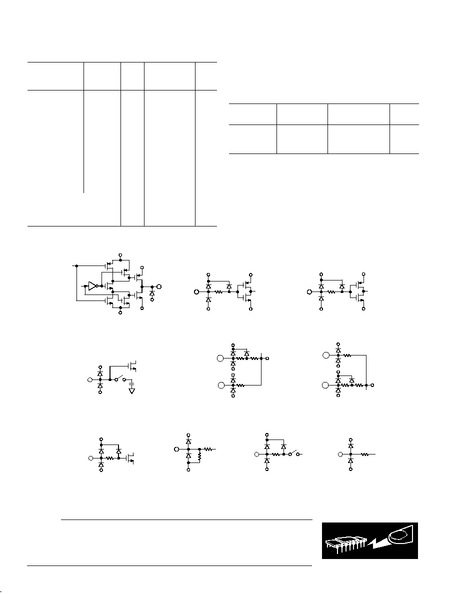
1
See Figures 1a and 1b.
Specifications subject to change without notice.
AD9280
REFTS
REFBS
MODE
AV
DD
10k
10k
0.4 V
DD
AD9280
REFTS
REFBF
MODE
REFTF
REFBS
4.2k
a.
b.
Figure 1. Equivalent Input Load
AD9280
≠3≠
REV. D
AD9280
≠4≠
REV. D
ABSOLUTE MAXIMUM RATINGS*
With
Respect
Parameter
to
Min
Max
Units
AVDD
AVSS
≠0.3
+6.5
V
DRVDD
DRVSS
≠0.3
+6.5
V
AVSS
DRVSS
≠0.3
+0.3
V
AVDD
DRVDD
≠6.5
+6.5
V
MODE
AVSS
≠0.3
AVDD + 0.3
V
CLK
AVSS
≠0.3
AVDD + 0.3
V
Digital Outputs
DRVSS
≠0.3
DRVDD + 0.3 V
AIN
AVSS
≠0.3
AVDD + 0.3
V
VREF
AVSS
≠0.3
AVDD + 0.3
V
REFSENSE
AVSS
≠0.3
AVDD + 0.3
V
REFTF, REFTB
AVSS
≠0.3
AVDD + 0.3
V
REFTS, REFBS
AVSS
≠0.3
AVDD + 0.3
V
Junction Temperature
+150
∞
C
Storage Temperature
≠65
+150
∞
C
Lead Temperature
10 sec
+300
∞
C
*Stresses above those listed under Absolute Maximum Ratings may cause perma-
nent damage to the device. This is a stress rating only; functional operation of the
device at these or any other conditions above those indicated in the operational
sections of this specification is not implied. Exposure to absolute maximum
ratings for extended periods may effect device reliability.
ORDERING GUIDE
Temperature
Package
Package
Model
Range
Description
Option*
AD9280ARS
≠40
∞
C to +85
∞
C 28-Lead SSOP
RS-28
AD9280ARSRL ≠40
∞
C to +85
∞
C 28-Lead SSOP (Reel) RS-28
AD9280-EB
Evaluation Board
*RS = Shrink Small Outline.
Figure 2. Equivalent Circuits
f. CLAMPIN
g. MODE
h. REFSENSE
i. VREF
CAUTION
ESD (electrostatic discharge) sensitive device. Electrostatic charges as high as 4000 V readily
accumulate on the human body and test equipment and can discharge without detection.
Although the AD9280 features proprietary ESD protection circuitry, permanent damage may
occur on devices subjected to high energy electrostatic discharges. Therefore, proper ESD
precautions are recommended to avoid performance degradation or loss of functionality.
WARNING!
ESD SENSITIVE DEVICE
DRVDD
AVSS
DRVSS
DRVSS
AVDD
AVDD
AVSS
AVSS
AVDD
22
21
REFTF
REFTS
AVDD
AVSS
AVDD
AVSS
25
24
REFBS
REFBF
AVDD
AVSS
AVDD
AVSS
AVDD
AVSS
AVDD
AVSS
AVSS
AVDD
AVSS
AVDD
AVDD
AVSS
AVDD
AVSS
AVDD
AVSS
a. D0≠D7, OTR
b. Three-State, Standby, Clamp
c. CLK
d. AIN
e. Reference

AD9280
≠5≠
REV. D
PIN CONFIGURATION
PIN FUNCTION DESCRIPTIONS
SSOP
Pin No.
Name
Description
1
AVSS
Analog Ground
2
DRVDD
Digital Driver Supply
3
NC
No Connect
4
NC
No Connect
5
D0
Bit 0
6
D1
Bit 1
7
D2
Bit 2
8
D3
Bit 3
9
D4
Bit 4
10
D5
Bit 5
11
D6
Bit 6
12
D7
Bit 7, Most Significant Bit
13
OTR
Out-of-Range Indicator
14
DRVSS
Digital Ground
15
CLK
Clock Input
16
THREE-STATE
HI: High Impedance State. LO: Normal Operation
17
STBY
HI: Power-Down Mode. LO: Normal Operation
18
REFSENSE
Reference Select
19
CLAMP
HI: Enable Clamp Mode. LO: No Clamp
20
CLAMPIN
Clamp Reference Input
21
REFTS
Top Reference
22
REFTF
Top Reference Decoupling
23
MODE
Mode Select
24
REFBF
Bottom Reference Decoupling
25
REFBS
Bottom Reference
26
VREF
Internal Reference Output
27
AIN
Analog Input
28
AVDD
Analog Supply
28-Lead Wide Body (SSOP)
14
13
12
11
10
9
8
1
2
3
4
7
6
5
TOP VIEW
(Not to Scale)
17
16
15
20
19
18
28
27
26
25
24
23
22
21
AD9280
AVSS
REFBS
VREF
AIN
AVDD
DRVDD
NC
NC
REFTF
MODE
REFBF
D0
D1
D2
D3
D4
D5
CLAMP
CLAMPIN
REFTS
D6
D7
OTR
DRVSS
REFSENSE
CLK
THREE-STATE
STBY
NC = NO CONNECT