 | ÐлекÑÑоннÑй компоненÑ: AD9281-EB | СкаÑаÑÑ:  PDF PDF  ZIP ZIP |
Äîêóìåíòàöèÿ è îïèñàíèÿ www.docs.chipfind.ru
AD9281
One Technology Way, P.O. Box 9106, Norwood, MA 02062-9106, U.S.A.
Tel: 781/329-4700
World Wide Web Site: http://www.analog.com
Fax: 781/326-8703
© Analog Devices, Inc., 1999
REV. E
Information furnished by Analog Devices is believed to be accurate and
reliable. However, no responsibility is assumed by Analog Devices for its
use, nor for any infringements of patents or other rights of third parties
which may result from its use. No license is granted by implication or
otherwise under any patent or patent rights of Analog Devices.
a
Dual Channel 8-Bit
Resolution CMOS ADC
FEATURES
Complete Dual Matching ADC
Low Power Dissipation: 225 mW (+3 V Supply)
Single Supply: 2.7 V to 5.5 V
Differential Nonlinearity Error: 0.1 LSB
On-Chip Analog Input Buffers
On-Chip Reference
Signal-to-Noise Ratio: 49.2 dB
Over Seven Effective Bits
Spurious-Free Dynamic Range: 65 dB
No Missing Codes Guaranteed
28-Lead SSOP
FUNCTIONAL BLOCK DIAGRAM
1V
REFERENCE
BUFFER
QREFB
IREFB
QREFT
IREFT
VREF
REFSENSE
IINA
IINB
"I" ADC
QINB
QINA
"Q" ADC
Q
REGISTER
I
REGISTER
THREE-
STATE
OUTPUT
BUFFER
AVDD
AVSS
CLOCK
DVDD
DVSS
SLEEP
SELECT
DATA
8 BITS
CHIP
SELECT
AD9281
ASYNCHRONOUS
MULTIPLEXER
PRODUCT DESCRIPTION
The AD9281 is a complete dual channel, 28 MSPS, 8-bit
CMOS ADC. The AD9281 is optimized specifically for applica-
tions where close matching between two ADCs is required (e.g.,
I/Q channels in communications applications). The 28 MHz
sampling rate and wide input bandwidth will cover both narrow-
band and spread-spectrum channels. The AD9281 integrates
two 8-bit, 28 MSPS ADCs, two input buffer amplifiers, an internal
voltage reference and multiplexed digital output buffers.
Each ADC incorporates a simultaneous sampling sample-and-
hold amplifier at its input. The analog inputs are buffered; no
external input buffer op amp will be required in most applica-
tions. The ADCs are implemented using a multistage pipeline
architecture that offers accurate performance and guarantees no
missing codes. The outputs of the ADCs are ported to a multi-
plexed digital output buffer.
The AD9281 is manufactured on an advanced low cost CMOS
process, operates from a single supply from 2.7 V to 5.5 V, and
consumes 225 mW of power (on 3 V supply). The AD9281
input structure accepts either single-ended or differential signals,
providing excellent dynamic performance up to and beyond
14 MHz Nyquist input frequencies.
PRODUCT HIGHLIGHTS
1. Dual 8-Bit, 28 MSPS ADC
A pair of high performance 28 MSPS ADCs that are opti-
mized for spurious free dynamic performance are provided for
encoding of I and Q or diversity channel information.
2. Low Power
Complete CMOS Dual ADC function consumes a low
225 mW on a single supply (on 3 V supply). The AD9281
operates on supply voltages from 2.7 V to 5.5 V.
3. On-Chip Voltage Reference
The AD9281 includes an on-chip compensated bandgap
voltage reference pin programmable for 1 V or 2 V.
4. On-chip analog input buffers eliminate the need for external
op amps in most applications.
5. Single 8-Bit Digital Output Bus
The AD9281 ADC outputs are interleaved onto a single
output bus saving board space and digital pin count.
6. Small Package
The AD9281 offers the complete integrated function in a
compact 28-lead SSOP package.
7. Product Family
The AD9281 dual ADC is pin compatible with a dual 10-bit
ADC (AD9201).

2
REV. E
AD9281SPECIFICATIONS
(AVDD = +3 V, DVDD = +3 V, F
SAMPLE
= 28 MSPS, VREF = 2 V, INB = 0.5 V, T
MIN
to T
MAX
unless otherwise noted)
Parameter
Symbol
Min
Typ
Max
Units
Condition
RESOLUTION
8
Bits
CONVERSION RATE
F
S
28
MHz
(32 MHz at +25
°
C)
DC ACCURACY
Differential Nonlinearity
DNL
±
0.1
LSB
REFT = 1.0 V, REFB = 0.0 V
Integral Nonlinearity
INL
±
0.25
LSB
Differential Nonlinearity (SE)
1
DNL
±
0.2
±
1.0
LSB
REFT = 1.0 V, REFB = 0.0 V
Integral Nonlinearity (SE)
1
INL
±
0.3
±
1.5
LSB
Zero-Scale Error, Offset Error
E
ZS
±
1
±
3.2
% FS
Full-Scale Error, Gain Error
E
FS
±
1.2
±
5.4
% FS
Gain Match
±
0.2
LSB
Offset Match
±
1.2
LSB
ANALOG INPUT
Input Voltage Range
AIN
0.5
AVDD/2
V
Input Capacitance
C
IN
2
pF
Aperture Delay
t
AP
4
ns
Aperture Uncertainty (Jitter)
t
AJ
2
ps
Aperture Delay Match
2
ps
Input Bandwidth (3 dB)
BW
Small Signal (20 dB)
240
MHz
Full Power (0 dB)
245
MHz
INTERNAL REFERENCE
Output Voltage (1 V Mode)
VREF
1
V
REFSENSE = VREF
Output Voltage Tolerance (1 V Mode)
±
10
mV
Output Voltage (2 V Mode)
VREF
2
V
REFSENSE = GND
Output Voltage Tolerance (2 V Mode)
±
15
mV
Load Regulation (1 V Mode)
VREF
±
10
±
35
mV
1 mA Load Current
Load Regulation (2 V Mode)
±
15
mV
1 mA Load Current
POWER SUPPLY
Operating Voltage
AVDD
2.7
3
5.5
V
DVDD
2.7
3
5.5
V
Supply Current
I
AVDD
75
mA
I
DVDD
0.1
mA
Power Consumption
P
D
225
260
mW
Power-Down
16
mW
STBY = AVDD, Clock Low
Power Supply Rejection
PSR
0.15
0.75
% FS
DYNAMIC PERFORMANCE
2
Signal-to-Noise and Distortion
SINAD
f = 3.58 MHz
46.4
49.1
dB
f = 14 MHz
48
dB
Signal-to-Noise
SNR
f = 3.58 MHz
47.8
49.2
dB
f = 14 MHz
48.5
dB
Total Harmonic Distortion
THD
f = 3.58 MHz
67.5
49.5
dB
f = 14 MHz
60
dB
Spurious Free Dynamic Range
SFDR
f = 3.58 MHz
49.6
65
dB
f = 14 MHz
56
dB
Two-Tone Intermodulation Distortion
3
IMD
58
dB
f = 44.9 MHz and 45.52 MHz
Differential Phase
DP
0.2
Degree
NTSC 40 IRE Mod Ramp
Differential Gain
DG
0.08
%
F
S
= 14.3 MHz
Crosstalk Rejection
62
dB
3
REV. E
AD9281
Parameter
Symbol
Min
Typ
Max
Units
Condition
DYNAMIC PERFORMANCE (SE)
1
Signal-to-Noise and Distortion
SINAD
f = 3.58 MHz
47.2
dB
Signal-to-Noise
SNR
f = 3.58 MHz
48
dB
Total Harmonic Distortion
THD
f = 3.58 MHz
55
dB
Spurious Free Dynamic Range
SFDR
f = 3.58 MHz
58
dB
DIGITAL INPUTS
High Input Voltage
V
IH
2.4
V
Low Input Voltage
V
IL
0.3
V
DC Leakage Current
I
IN
±
6
µ
A
Input Capacitance
C
IN
2
pF
LOGIC OUTPUT (with DVDD = 3 V)
High Level Output Voltage
(I
OH
= 50
µ
A)
V
OH
2.88
V
Low Level Output Voltage
(I
OL
= 1.5 mA)
V
OL
0.095
V
LOGIC OUTPUT (with DVDD = 5 V)
High Level Output Voltage
(I
OH
= 50
µ
A)
V
OH
4.5
V
Low Level Output Voltage
(I
OL
= 1.5 mA)
V
OL
0.4
V
Data Valid Delay
t
OD
11
ns
MUX Select Delay
t
MD
7
ns
Data Enable Delay
t
ED
13
ns
C
L
= 20 pF. Output Level to
90% of Final Value
Data High-Z Delay
t
DHZ
13
ns
CLOCKING
Clock Pulsewidth High
t
CH
16.9
ns
Clock Pulsewidth Low
t
CL
16.9
ns
Pipeline Latency
3.0
Cycles
NOTES
1
SE is single ended input, REFT = 1.5 V, REFB = 0.5 V.
2
AIN differential 2 V p-p, REFT = 1.5 V, REFB = 0.5 V.
3
IMD referred to larger of two input signals.
Specifications subject to change without notice.
CLOCK
INPUT
SELECT
INPUT
DATA
OUTPUT
ADC SAMPLE
#2
ADC SAMPLE
#3
ADC SAMPLE
#4
ADC SAMPLE
#5
Q CHANNEL
OUTPUT ENABLED
I CHANNEL
OUTPUT ENABLED
SAMPLE #1-3
Q CHANNEL
OUTPUT
SAMPLE #1-2
Q CHANNEL
OUTPUT
SAMPLE #1-1
Q CHANNEL
OUTPUT
SAMPLE #1-1
I CHANNEL
OUTPUT
SAMPLE #1
Q CHANNEL
OUTPUT
SAMPLE #1
I CHANNEL
OUTPUT
SAMPLE #2
Q CHANNEL
OUTPUT
t
MD
t
OD
ADC SAMPLE
#1
Figure 1. ADC Timing
AD9281
4
REV. E
CAUTION
ESD (electrostatic discharge) sensitive device. Electrostatic charges as high as 4000 V readily
accumulate on the human body and test equipment and can discharge without detection.
Although the AD9281 features proprietary ESD protection circuitry, permanent damage may
occur on devices subjected to high energy electrostatic discharges. Therefore, proper ESD
precautions are recommended to avoid performance degradation or loss of functionality.
PIN CONFIGURATION
TOP VIEW
(Not to Scale)
AD9281
REFT-Q
INB-Q
INA-Q
CHIP-SELECT
VREF
AVDD
REFB-Q
REFB-I
AVSS
REFSENSE
REFT-I
SLEEP
INA-I
INB-I
DVSS
DVDD
NC
NC
(LSB) D0
D1
D2
D3
D4
D5
D6
(MSB) D7
SELECT
CLOCK
NC = NO CONNECT
WARNING!
ESD SENSITIVE DEVICE
ABSOLUTE MAXIMUM RATINGS*
With
Respect
Parameter
to
Min
Max
Units
AVDD
AVSS
0.3
+6.5
V
DVDD
DVSS
0.3
+6.5
V
AVSS
DVSS
0.3
+0.3
V
AVDD
DVDD
6.5
+6.5
V
CLK
AVSS
0.3
AVDD + 0.3
V
Digital Outputs
DVSS
0.3
DVDD + 0.3
V
AINA, AINB
AVSS
1.0
AVDD + 0.3
V
VREF
AVSS
0.3
AVDD + 0.3
V
REFSENSE
AVSS
0.3
AVDD + 0.3
V
REFT, REFB
AVSS
0.3
AVDD + 0.3
V
Junction Temperature
+150
°
C
Storage Temperature
65
+150
°
C
Lead Temperature
10 sec
+300
°
C
*Stresses above those listed under Absolute Maximum Ratings may cause perma-
nent damage to the device. This is a stress rating only; functional operation of the
device at these or any other conditions above those indicated in the operational
sections of this specification is not implied. Exposure to absolute maximum ratings
for extended periods may effect device reliability.
ORDERING GUIDE
Temperature
Package
Package
Model
Range
Description
Options*
AD9281ARS
40
°
C to +85
°
C
28-Lead SSOP
RS-28
AD9281-EB
Evaluation Board
*RS = Shrink Small Outline.
PIN FUNCTION DESCRIPTIONS
P
in
No.
Name
Description
1
DVSS
Digital Ground
2
DVDD
Digital Supply
3
NC
Not Connected
4
NC
Not Connected
5
D0
Bit 0 (LSB)
6
D1
Bit 1
7
D2
Bit 2
8
D3
Bit 3
9
D4
Bit 4
10
D5
Bit 5
11
D6
Bit 6
12
D7
Bit 7 (MSB)
13
SELECT
Hi I Channel Out, Lo Q Channel Out
14
CLOCK
Clock
15
SLEEP
Hi Power Down, Lo Normal Operation
16
INA-I
I Channel, A Input
17
INB-I
I Channel, B Input
18
REFT-I
Top Reference Decoupling, I Channel
19
REFB-I
Bottom Reference Decoupling, I Channel
20
AVSS
Analog Ground
21
REFSENSE
Reference Select
22
VREF
Internal Reference Output
23
AVDD
Analog Supply
24
REFB-Q
Bottom Reference Decoupling, Q Channel
25
REFT-Q
Top Reference Decoupling, Q Channel
26
INB-Q
Q Channel B Input
27
INA-Q
Q Channel A Input
28
CHIP-SELECT
Hi-High Impedance, Lo-Normal Operation
DEFINITIONS OF SPECIFICATIONS
INTEGRAL NONLINEARITY (INL)
Integral nonlinearity refers to the deviation of each individual
code from a line drawn from "zero" through "full scale." The
point used as "zero" occurs 1/2 LSB before the first code transi-
tion. "Full scale" is defined as a level 1 1/2 LSBs beyond the last
code transition. The deviation is measured from the center of
each particular code to the true straight line.
DIFFERENTIAL NONLINEARITY (DNL, NO MISSING
CODES)
An ideal ADC exhibits code transitions that are exactly 1 LSB
apart. DNL is the deviation from this ideal value. It is often
specified in terms of the resolution for which no missing codes
(NMC) are guaranteed.
AD9281
5
REV. E
DRVDD
AVSS
DRVSS
DRVSS
AVDD
AVDD
AVSS
AVSS
AVDD
REFBS
REFBF
AVDD
AVSS
AVDD
AVSS
AVDD
AVSS
AVDD
AVSS
IN
AVDD
AVSS
AVSS
AVDD
AVDD
AVSS
AVDD
AVSS
d. INA, INB
e. Reference
f. REFSENSE
g. VREF
Figure 2. Equivalent Circuits
OFFSET ERROR
The first transition should occur at a level 1 LSB above "zero."
Offset is defined as the deviation of the actual first code transi-
tion from that point.
OFFSET MATCH
The change in offset error between I and Q channels.
EFFECTIVE NUMBER OF BITS (ENOB)
For a sine wave, SINAD can be expressed in terms of the num-
ber of bits. Using the following formula,
N = (SINAD 1.76)/6.02
It is possible to get a measure of performance expressed as N,
the effective number of bits.
Thus, effective number of bits for a device for sine wave inputs
at a given input frequency can be calculated directly from its
measured SINAD.
TOTAL HARMONIC DISTORTION (THD)
THD is the ratio of the rms sum of the first six harmonic com-
ponents to the rms value of the measured input signal and
is expressed as a percentage or in decibels.
SIGNAL-TO-NOISE RATIO (SNR)
SNR is the ratio of the rms value of the measured input signal
to the rms sum of all other spectral components below the
Nyquist frequency, excluding the first six harmonics and dc.
The value for SNR is expressed in decibels.
SPURIOUS FREE DYNAMIC RANGE (SFDR)
The difference in dB between the rms amplitude of the input
signal and the peak spurious signal.
GAIN ERROR
The first code transition should occur for an analog value 1 LSB
above nominal negative full scale. The last transition should
occur for an analog value 1 LSB below the nominal positive full
scale. Gain error is the deviation of the actual difference be-
tween first and last code transitions and the ideal difference
between the first and last code transitions.
GAIN MATCH
The change in gain error between I and Q channels.
PIPELINE DELAY (LATENCY)
The number of clock cycles between conversion initiation and
the associated output data being made available. New output
data is provided every rising clock edge.
MUX SELECT DELAY
The delay between the change in SELECT pin data level and
valid data on output pins.
POWER SUPPLY REJECTION
The specification shows the maximum change in full scale from
the value with the supply at the minimum limit to the value
with the supply at its maximum limit.
APERTURE JITTER
Aperture jitter is the variation in aperture delay for successive
samples and is manifested as noise on the input to the A/D.
APERTURE DELAY
Aperture delay is a measure of the Sample-and-Hold Amplifier
(SHA) performance and is measured from the rising edge of the
clock input to when the input signal is held for conversion.
SIGNAL-TO-NOISE AND DISTORTION (S/N+D, SINAD)
RATIO
S/N+D is the ratio of the rms value of the measured input sig-
nal to the rms sum of all other spectral components below
the Nyquist frequency, including harmonics but excluding dc.
The value for S/N+D is expressed in decibels.
a. D0D9 b. Three-State Standby c. CLK
AD9281
6
REV. E
Typical Characteristic Curves
(AVDD = +3 V, DVDD = +3 V, F
S
= 28 MHz (50% duty cycle), 2 V input span from 0.5 V to +1.5 V, 2 V internal reference unless otherwise noted)
CODE OFFSET
1
1
0
LSB
0
16 32 48 64 80 96 112 128 144 160 176 192 208 224 240
Figure 3. Typical INL
CODE OFFSET
1
1
0
LSB
0
16 32 48 64 80 96 112 128 144 160 176 192 208 224 240
Figure 4. Typical DNL
INPUT VOLTAGE Volts
1.00
1.00
1.0
2.0
0.5
I
B
nA
0
0.5
1.0
1.5
0.80
0.20
0.40
0.60
0.80
0.60
0.40
0.00
0.20
Figure 5. Input Bias Current vs. Input Voltage
INPUT FREQUENCY Hz
55
1.0E+05
SNR dB
50
45
40
35
30
25
1.0E+06
1.0E+07
1.0E+08
0.5dB
6dB
20dB
Figure 6. SNR vs. Input Frequency
INPUT FREQUENCY Hz
55
1.0E+05
SNR dB
50
45
40
35
30
25
1.0E+06
1.0E+07
1.0E+08
0.5dB
6dB
20dB
Figure 7. SINAD vs. Input Frequency
INPUT FREQUENCY Hz
30
1.0E+05
THD dB
35
40
45
50
55
60
1.0E+06
1.0E+07
1.0E+08
65
70
0.5dB
6dB
20dB
Figure 8. THD vs. Input Frequency
AD9281
7
REV. E
CLOCK FREQUENCY Hz
70
20
1.00E+06
1.00E+08
1.00E+07
THD dB
55
65
60
50
45
40
35
30
25
Figure 9. THD vs. Clock Frequency
TEMPERATURE C
1.013
1.012
1.008
40
100
20
V
REF
Volts
0
20
40
60
80
1.011
1.010
1.009
Figure 10. Voltage Reference Error vs. Temperature
CLOCK FREQUENCY MHz
185
0
32
4
POWER CONSUMPTION mW
8
12
16
20
24
28
220
210
200
190
240
230
225
215
205
235
195
Figure 11. Power Consumption vs. Clock Frequency
CODE
1.20E+07
1.00E+07
0.00E+00
N+1
N1
HITS
N
8.00E+06
6.00E+06
4.00E+06
2.00E+06
12050
10000000
800
Figure 12. Grounded Input Histogram
INPUT FREQUENCY Hz
0
1.00E+06
AMPLITUDE dB
3
6
9
12
15
21
1.00E+07
1.00E+08
1.00E+09
24
27
18
Figure 13. Full Power Bandwidth
INPUT FREQUENCY Hz
50
1.00E+05
SNR dB
45
40
35
30
25
1.00E+06
1.00E+07
1.00E+08
0.5dB
6dB
20dB
Figure 14. SNR vs. Input Frequency (Single-Ended)
AD9281
8
REV. E
THEORY OF OPERATION
The AD9281 integrates two A/D converters, two analog input
buffers, an internal reference and reference buffer, and an out-
put multiplexer. For clarity, this data sheet refers to the two
converters as "I" and "Q." The two A/D converters simulta-
neously sample their respective inputs on the rising edge of the
input clock. The two converters distribute the conversion opera-
tion over several smaller A/D sub-blocks, refining the conversion
with progressively higher accuracy as it passes the result from
stage to stage. As a consequence of the distributed conversion,
each converter requires a small fraction of the 256 comparators
used in a traditional flash-type 8-bit ADC. A sample-and-hold
function within each of the stages permits the first stage to oper-
ate on a new input sample while the following stages continue to
process previous samples. This results in a "pipeline processing"
latency of three clock periods between when an input sample is
taken and when the corresponding ADC output is updated into
the output registers.
The AD9281 integrates input buffer amplifiers to drive the
analog inputs of the converters. In most applications, these
input amplifiers eliminate the need for external op amps for the
input signals. The input structure is fully differential, but the
SHA common-mode response has been designed to allow the
converter to readily accommodate either single-ended or differ-
ential input signals. This differential structure makes the part
capable of accommodating a wide range of input signals.
The AD9281 also includes an on-chip bandgap reference and
reference buffer. The reference buffer shifts the ground-referred
reference to levels more suitable for use by the internal circuits
of the converter. Both converters share the same reference and
reference buffer. This scheme provides for the best possible gain
match between the converters while simultaneously minimizing
the channel-to-channel crosstalk.
Each A/D converter has its own output latch, which updates on
the rising edge of the input clock. A logic multiplexer, con-
trolled through the SELECT pin, determines which channel is
passed to the digital output pins. The output drivers have their
own supply, allowing the part to be interfaced to a variety of
logic families. The outputs can be placed in a high impedance
state using the CHIP SELECT pin.
The AD9281 has great flexibility in its supply voltage. The
analog and digital supplies may be operated from 2.7 V to 5.5 V,
independently of one another.
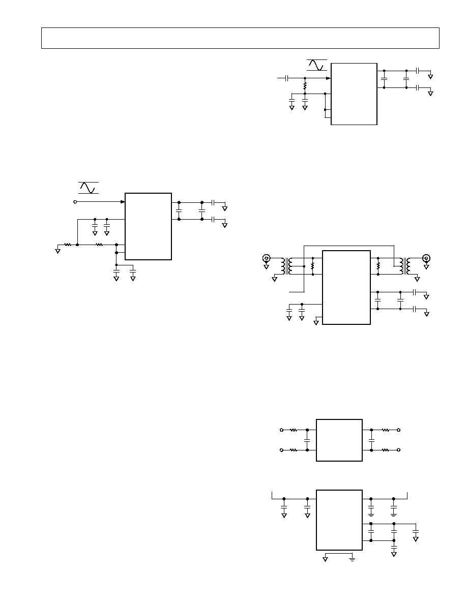
ANALOG INPUT
Figure 16 shows an equivalent circuit structure for the analog
input of one of the A/D converters. PMOS source-followers
buffer the analog input pins from the charge kickback problems
normally associated with switched capacitor ADC input struc-
tures. This produces a very high input impedance on the part,
allowing it to be effectively driven from high impedance sources.
This means that the AD9281 could even be driven directly by a
passive antialias filter.
ADC
CORE
+FS
LIMIT
FS
LIMIT
BUFFER
BUFFER
IINA
IINB
V
REF
+FS LIMIT =
V
REF
+V
REF/2
FS LIMIT =
V
REF
V
REF/2
OUTPUT
WORD
SHA
Figure 16. Equivalent Circuit for AD9281 Analog Inputs
The source followers inside the buffers also provide a level-shift
function of approximately 1 V, allowing the AD9281 to accept
inputs at or below ground. One consequence of this structure is
that distortion will result if the analog input comes within 1.4 V
of the positive supply. For optimum high frequency distortion
performance, the analog input signal should be centered accord-
ing to Figure 27.
The capacitance load of the analog input pin is 4 pF to the
analog supplies (AVSS, AVDD).
Full-scale setpoints may be calculated according to the following
algorithm (V
REF
may be internally or externally generated):
F
S
= V
REF
(V
REF
/2)
+F
S
= V
REF
+ (V
REF
/2)
V
SPAN
= V
REF
10.0
0.0E+0
SNR dB
0.0
10.0
20.0
30.0
40.0
50.0
60.0
70.0
80.0
90.0
100.0
110.0
2.0E+6
4.0E+6
6.0E+6
8.0E+6 10.0E+6 12.0E+6 14.0E+6
FUND
5TH
6TH
4TH
7TH
3RD
9TH
2ND
8TH
Figure 15a. Simultaneous Operation of I and Q Channels
10.0
0.0E+0
SNR dB
0.0
10.0
20.0
30.0
40.0
50.0
60.0
70.0
80.0
90.0
100.0
110.0
2.0E+6
4.0E+6
6.0E+6
8.0E+6 10.0E+6 12.0E+6 14.0E+6
FUND
5TH
4TH
7TH
3RD
2ND
8TH
6TH
Figure 15b. Simultaneous Operation of I and Q Channels
AD9281
9
REV. E
The AD9281 can accommodate a variety of input spans be-
tween 1 V and 2 V. For spans of less than 1 V, expect a propor-
tionate degradation in SNR. Use of a 2 V span will provide the
best noise performance. 1 V spans will provide lower distortion
when using a 3 V analog supply. Users wishing to run with larger
full-scales are encouraged to use a 5 V analog supply (AVDD).
Single-Ended Inputs:
For single-ended input signals, the
signal is applied to one input pin and the other input pin is tied
to a midscale voltage. This midscale voltage defines the center
of the full-scale span for the input signal.
EXAMPLE: For a single-ended input range from 0 V to 1 V
applied to IINA, we would configure the converter for a 1 V
reference (see Figure 17) and apply 0.5 V to IINB.
I OR QREFT
I OR QREFB
IINA
IINB
VREF
REF SENSE
0.1 F
10 F
0.1 F
0.1 F
0.1 F
AD9281
0.1 F
10 F
10 F
MIDSCALE
VOLTAGE
= 0.5V (1V)
1V
0V
INPUT
5k
5k
Figure 17. Example Configuration for 0 V1 V Single-
Ended Input Signal
Note that since the inputs are high impedance, this reference
level can easily be generated with an external resistive divider
with large resistance values (to minimize power dissipation). A
decoupling capacitor is recommended on this input to minimize
the high frequency noise-coupling onto this pin. Decoupling
should occur close to the ADC.
Differential Inputs
Use of differential input signals can provide greater flexibility in
input ranges and bias points, as well as offering improvements in
distortion performance, particularly for high frequency input
signals. Users with differential input signals will probably want
to take advantage of the differential input structure of the AD9281.
Performance is still very good for single-ended inputs. Convert-
ing a single-ended input to a differential signal for application to
the converter is probably only worth considering for very high
frequency input signals.
AC-Coupled Inputs
If the signal of interest has no dc component, ac coupling can be
easily used to define an optimum bias point. Figure 18 illustrates
one recommended configuration. The voltage chosen for the dc
bias point (in this case the 1 V reference) is applied to both
IINA and IINB pins through 1 k
resistors (R1 and R2). IINA
is coupled to the input signal through Capacitor C1, while IINB is
decoupled to ground through Capacitor C2.
0.1 F
10 F
0.1 F
0.1 F
ANALOG
INPUT
1.0 F
0.1 F
1k
1.5V
0.5V
I OR QREFT
I OR QREFB
IINA
IINB
VREF
AD9281
REFSENSE
Figure 18. Example Configuration for 0.5 V1.5 V ac
Coupled Single-Ended Inputs
Transformer Coupled Inputs
Another option for input ac coupling is to use a transformer.
This not only provides dc rejection, but also allows truly differ-
ential drive of the AD9281's analog inputs, which will provide
the optimal distortion performance. Figure 19 shows a recom-
mended transformer input drive configuration. Resistors R1 and
R2 define the termination impedance of the transformer cou-
pling. The center tap of the transformer secondary is tied to the
common-mode voltage, establishing the dc bias point for the
analog inputs.
0.1 F
10 F
0.1 F
0.1 F
COMMON
MODE
VOLTAGE
0.1 F
10 F
R1
R2
I OR QREFT
I OR QREFB
IINA
IINB
AD9281
QINB
QINA
REFSENSE
VREF
Figure 19. Example Configuration for Transformer
Coupled Inputs
Crosstalk:
The internal layout of the AD9281, as well as its
pinout, was configured to minimize the crosstalk between the
two input signals. Users wishing to minimize high frequency
crosstalk should take care to provide the best possible decoupling
for input pins (see Figure 20). R and C values will make a pole
dependant on antialiasing requirements. Decoupling is also
required on reference pins and power supplies (see Figure 21).
QINA
QINB
IINA
IINB
AD9281
Figure 20. Input Loading
DVDD
I OR QREFT
I OR QREFB
AVDD
0.1 F
10 F
0.1 F
10 F
AD9281
0.1 F
0.1 F
0.1 F
10 F
V ANALOG
V DIGITAL
Figure 21. Reference and Power Supply Decoupling
AD9281
10
REV. E
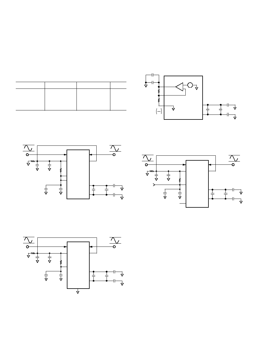
REFERENCE AND REFERENCE BUFFER
The reference and buffer circuitry on the AD9281 is configured
for maximum convenience and flexibility. An illustration of the
equivalent reference circuit is show in Figure 26. The user can
select from five different reference modes through appropriate
pin-strapping (see Table I below). These pin strapping options
cause the internal circuitry to reconfigure itself for the appropri-
ate operating mode.
Table I. Table of Modes
Mode
Input Span
REFSENSE Pin Figure
1 V
1 V
VREF
22
2 V
2 V
AGND
23
Programmable
1 + (R1/R2)
See Figure
24
External
= External Ref
AVDD
25
1 V Mode (Figure 22)
--provides a 1 V reference and 1 V input
full scale. Recommended for applications wishing to optimize
high frequency performance, or any circuit on a supply voltage
of less than 4 V. The part is placed in this mode by shorting the
REFSENSE pin to the VREF pin.
I OR QREFT
I OR QREFB
IINA
IINB
VREF
0.1 F
10 F
0.1 F
0.1 F
0.1 F
AD9281
0.1 F
10 F
10 F
1V
0V
QINB
QINA
5k
5k
REFSENSE
1V
0V
1V
Figure 22. 0 V to 1 V Input
2 V Mode (Figure 23)
--provides a 2 V reference and 2 V input
full scale. Recommended for noise sensitive applications on 5 V
supplies. The part is placed in 2 V reference mode by ground-
ing (shorting to AVSS) the REFSENSE pin.
I OR QREFT
I OR QREFB
IINA
IINB
VREF
0.1 F
10 F
0.1 F
0.1 F
0.1 F
AD9281
0.1 F
10 F
10 F
2V
0V
QINB
QINA
5k
5k
REFSENSE
2V
0V
Figure 23. 0 V to 2 V Input
Externally Set Voltage Mode (Figure 24)
--this mode uses
the on-chip reference, but scales the exact reference level though
the use of an external resistor divider network. VREF is wired to
the top of the network, with the REFSENSE wired to the tap
point in the resistor divider. The reference level (and input full
scale) will be equal to 1 V
× (R1 + R2)/R1. This method can be
used for voltage levels from 0.7 V to 2.5 V.
I OR QREFT
I OR QREFB
VREF
0.1 F
10 F
0.1 F
0.1 F
AD9281
REFSENSE
+
AVSS
0.1 F
1 F
R2
R1
1V
VREF = 1 +
R2
R1
+
Figure 24. Programmable Reference
External Reference Mode (Figure 25)
--in this mode, the on-
chip reference is disabled, and an external reference applied to
the VREF pin. This mode is achieved by tying the REFSENSE
pin to AVDD.
1V
EXT
REFERENCE
AVDD
I OR QREFT
I OR QREFB
IINA
IINB
VREF
0.1 F
10 F
0.1 F
0.1 F
0.1 F
AD9281
0.1 F
10 F
10 F
1V
0V
QINB
QINA
5k
5k
REFSENSE
1V
0V
Figure 25. External Reference
Reference Buffer
--The reference buffer structure takes the
voltage on the VREF pin and level-shifts and buffers it for use
by various sub-blocks within the two A/D converters. The two
converters share the same reference buffer amplifier to maintain
the best possible gain match between the two converters. In the
interests of minimizing high frequency crosstalk, the buffered
references for the two converters are separately decoupled on
the IREFB, IREFT, QREFB and QREFT pins, as illustrated in
Figure 26.
AD9281
11
REV. E
QREFT
QREFB
IREFT
0.1 F
10 F
0.1 F
0.1 F
AD9281
REFSENSE
AVSS
1V
0.1 F
10 F
IREFB
VREF
0.1 F
0.1 F
10k
10k
ADC
CORE
INTERNAL
CONTROL
LOGIC
0.1 F
1.0 F
Figure 26. Reference Buffer Equivalent Circuit and
External Decoupling Recommendation
For best results in both noise suppression and robustness
against crosstalk, the 4-capacitor buffer decoupling arrangement
shown in Figure 26 is recommended. This decoupling should
3
0.5
THD dB
13
23
33
43
53
63
73
0
0.5
1
1.5
CML V
2V
1V
a. Differential Input, 3 V Supplies
35
0.5
THD dB
40
45
50
55
60
65
70
0
0.5
1
1.5
CML V
2
2.5
1V
2V
b. Differential Input, 5 V Supplies
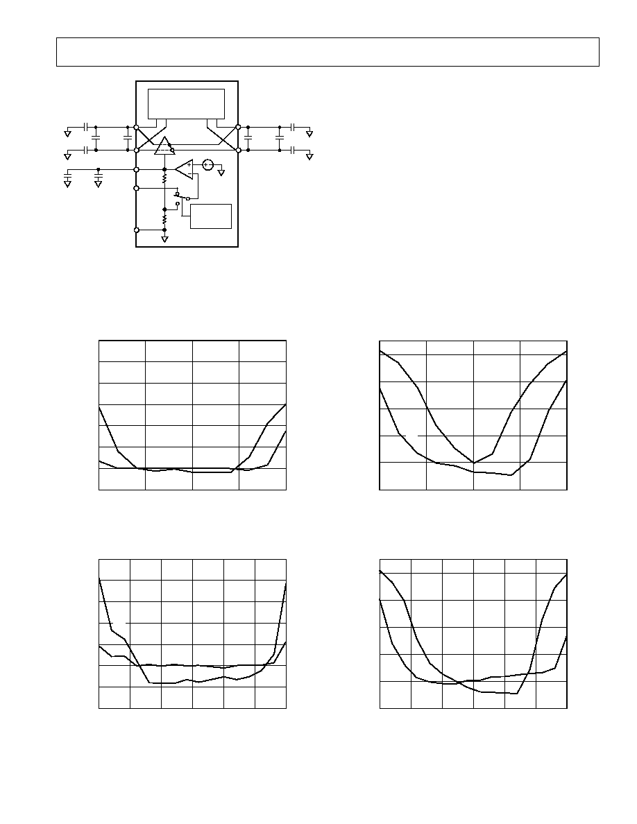
Figure 27. THD vs. CML Input Span and Power Supply (Analog Input = 1 MHz)
15
0.5
THD dB
25
35
45
55
65
0
0.5
1
1.5
CML V
2V
1V
c. Single-Ended Input, 3 V Supplies
15
0.5
THD dB
25
35
45
55
65
0
0.5
1
1.5
CML V
2V
1V
2
2.5
d. Single-Ended Input, 5 V Supplies
feature chip capacitors located close to the converter IC. The
capacitors are connected to either IREFT/IREFB or QREFT/
QREFB. A connection to both sides is not required.
COMMON-MODE PERFORMANCE
Attention to the common-mode point of the analog input volt-
age can improve the performance of the AD9281. Figure 27
illustrates THD as a function of common-mode voltage (center
point of the analog input span) and power supply.
Inspection of the curves will yield the following conclusions:
1. An AD9281 running with AVDD = 5 V is the easiest to
drive.
2. Differential inputs are the most insensitive to common-mode
voltage.
3. An AD9281 powered by AVDD = 3 V and a single ended
input, should have a 1 V span with a common-mode voltage
of 0.75 V.
AD9281
12
REV. E
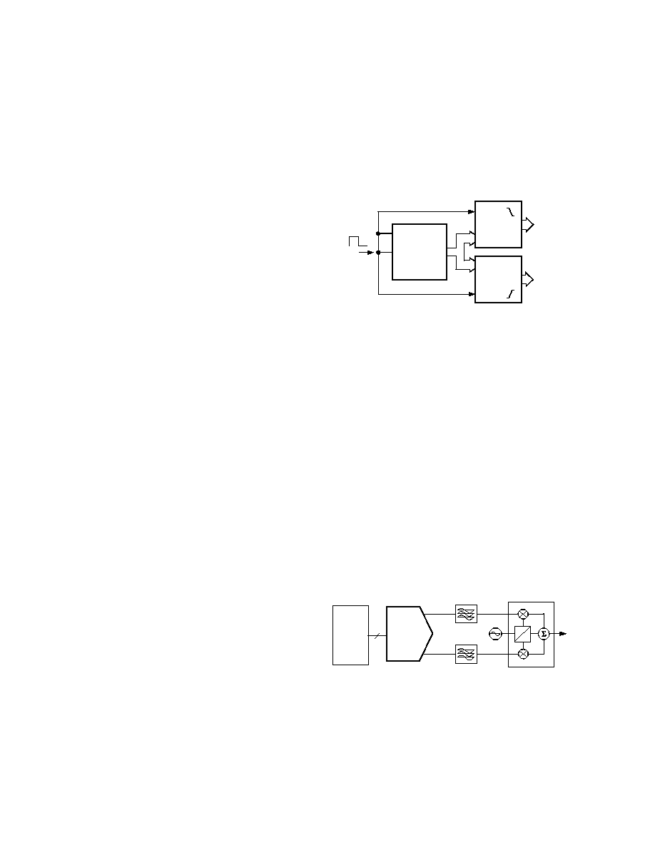
SELECT
When the select pin is held LOW, the output word will present
the "Q" level. When the select pin is held HIGH, the "I" level
will be presented to the output word (see Figure 1).
The AD9281's select and clock pins may be driven by a com-
mon signal source. The data will change in 5 ns to 11 ns after
the edges of the input pulse. The user must make sure the inter-
face latches have sufficient hold time for the AD9281's delays
(see Figure 28).
CLOCK
DATA
I LATCH
CLOCK
DATA
Q LATCH
CLK
DATA
OUT
SELECT
I
PROCESSING
Q
PROCESSING
CLOCK
SOURCE
Figure 28. Typical De-Mux Connection
APPLICATIONS
USING THE AD9281 FOR QAM DEMODULATION
QAM is one of the most widely used digital modulation schemes in
digital communication systems. This modulation technique
can be found in both FDMA as well as spread spectrum (i.e.,
CDMA) based systems. A QAM signal is a carrier frequency
which is both modulated in amplitude (i.e., AM modulation)
and in phase (i.e., PM modulation). At the transmitter, it can
be generated by independently modulating two carriers of iden-
tical frequency but with a 90
°
phase difference. This results in
an inphase (I) carrier component and a quadrature (Q) carrier
component at a 90
°
phase shift with respect to the I component.
The I and Q components are then summed to provide a QAM
signal at the specified carrier or IF frequency. Figure 29 shows
a typical analog implementation of a QAM modulator using a
dual 10-bit DAC with 2
× interpolation, the AD9761. A QAM
signal can also be synthesized in the digital domain thus requir-
ing a single DAC to reconstruct the QAM signal. The AD9853
is an example of a complete (i.e., DAC included) digital QAM
modulator.
0
90
DSP
OR
ASIC
10
CARRIER
FREQUENCY
NYQUIST
FILTERS
TO
MIXER
QUADRATURE
MODULATOR
AD9761
IOUT
QOUT
Figure 29. Typical Analog QAM Modulator Architecture
DIGITAL INPUTS AND OUTPUTS
Each of the AD9281 digital control inputs, CHIP SELECT,
CLOCK, SELECT and SLEEP are referenced to AVDD and
AVSS. Switching thresholds will be AVDD/2.
The format of the digital output is straight binary. A low power
mode feature is provided such that for STBY = HIGH and the
clock disabled, the static power of the AD9281 will drop below
22 mW.
CLOCK INPUT
The AD9281 clock input is internally buffered with an inverter
powered from the AVDD pin. This feature allows the AD9281
to accommodate either +5 V or +3.3 V CMOS logic input sig-
nal swings with the input threshold for the CLK pin nominally
at AVDD/2.
The pipelined architecture of the AD9281 operates on both
rising and falling edges of the input clock. To minimize duty
cycle variations the logic family recommended to drive the clock
input is high speed or advanced CMOS (HC/HCT, AC/ACT)
logic. CMOS logic provides both symmetrical voltage threshold
levels and sufficient rise and fall times to support 28 MSPS
operation. Running the part at slightly faster clock rates may be
possible, although at reduced performance levels. Conversely,
some slight performance improvements might be realized by
clocking the AD9281 at slower clock rates.
The power dissipated by the output buffers is largely propor-
tional to the clock frequency; running at reduced clock rates
provides a reduction in power consumption.
DIGITAL OUTPUTS
Each of the on-chip buffers for the AD9281 output bits (D0D9)
is powered from the DVDD supply pin, separate from AVDD.
The output drivers are sized to handle a variety of logic families
while minimizing the amount of glitch energy generated. In all
cases, a fan-out of one is recommended to keep the capacitive
load on the output data bits below the specified 20 pF level.
For DVDD = 5 V, the AD9281 output signal swing is compat-
ible with both high speed CMOS and TTL logic families. For
TTL, the AD9281 on-chip, output drivers were designed to
support several of the high speed TTL families (F, AS, S). For
applications where the clock rate is below 28 MSPS, other TTL
families may be appropriate. For interfacing with lower voltage
CMOS logic, the AD9281 sustains 28 MSPS operation with
DVDD = 3 V. In all cases, check your logic family data sheets
for compatibility with the AD9281's Specification table.
A 2 ns reduction in output delays can be achieved by limiting
the logic load to 5 pF per output line.
THREE-STATE OUTPUTS
The digital outputs of the AD9281 can be placed in a high
impedance state by setting the CHIP SELECT pin to HIGH.
This feature is provided to facilitate in-circuit testing or evaluation.
AD9281
13
REV. E
ANALOG
CIRCUITS
DIGITAL
LOGIC
ICs
V
A
A
D
DVSS
AVSS
A
B
I
A
I
D
AVDD
DVDD
LOGIC
SUPPLY
D
A
V
IN
C
STRAY
C
STRAY
GND
A
= ANALOG
D
= DIGITAL
ADC
IC
DIGITAL
CIRCUITS
A
A
Figure 31. Ground and Power Consideration
These characteristics result in both a reduction of electro-
magnetic interference (EMI) and an overall improvement in
performance.
It is important to design a layout that prevents noise from cou-
pling onto the input signal. Digital signals should not be run in
parallel with the input signal traces and should be routed
away from the input circuitry. Separate analog and digital
grounds should be joined together directly under the AD9281 in
a solid ground plane. The power and ground return currents
must be carefully managed. A general rule of thumb for mixed
signal layouts dictates that the return currents from digital cir-
cuitry should not pass through critical analog circuitry.
Transients between AVSS and DVSS will seriously degrade
performance of the ADC.
If the user cannot tie analog ground and digital ground together
at the ADC, he should consider the configuration in Figure 32.
Another input and ground technique is shown in Figure 32. A
separate ground plane has been split for RF or hard to manage
signals. These signals can be routed to the ADC differentially or
single ended (i.e., both can either be connected to the driver or
RF ground). The ADC will perform well with several hundred
mV of noise or signals between the RF and ADC analog ground.
DATA
ANALOG
GROUND
DIGITAL
GROUND
LOGIC
ADC
AIN
BIN
RF
GROUND
Figure 32. RF Ground Scheme
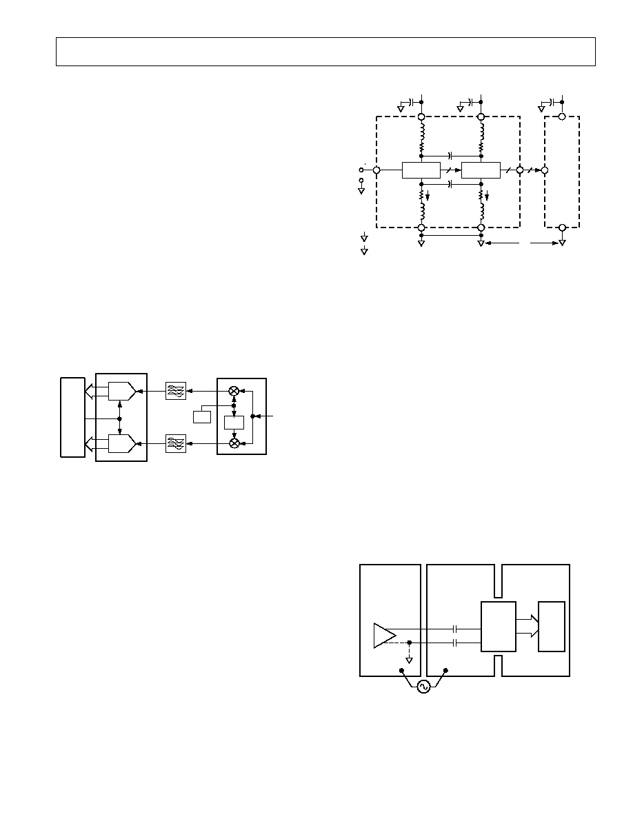
At the receiver, the demodulation of a QAM signal back into its
separate I and Q components is essentially the modulation
process explain above but in the reverse order. A common and
traditional implementation of a QAM demodulator is shown in
Figure 30. In this example, the demodulation is performed in
the analog domain using a dual, matched ADC and a quadra-
ture demodulator to recover and digitize the I and Q baseband
signals. The quadrature demodulator is typically a single IC
containing two mixers and the appropriate circuitry to generate
the necessary 90
°
phase shift between the I and Q mixers' local
oscillators. Before being digitized by the ADCs, the mixed
down baseband I and Q signals are filtered using matched ana-
log filters. These filters, often referred to as Nyquist or Pulse-
Shaping filters, remove images-from the mixing process and any
out-of-band. The characteristics of the matching Nyquist filters
are well defined to provide optimum signal-to-noise (SNR)
performance while minimizing intersymbol interference. The
ADC's are typically simultaneously sampling their respective
inputs at the QAM symbol rate or, most often, at a multiple of it
if a digital filter follows the ADC. Oversampling and the use of
digital filtering eases the implementation and complexity of the
analog filter. It also allows for enhanced digital processing for
both carrier and symbol recovery and tuning purposes. The use
of a dual ADC such as the AD9281 ensures excellent gain,
offset, and phase matching between the I and Q channels.
90°C
FROM
PREVIOUS
STAGE
QUADRATURE
DEMODULATOR
LO
I
ADC
DSP
OR
ASIC
CARRIER
FREQUENCY
NYQUIST
FILTERS
Q
ADC
DUAL MATCHED
ADC
Figure 30. Typical Analog QAM Demodulator
GROUNDING AND LAYOUT RULES
As is the case for any high performance device, proper ground-
ing and layout techniques are essential in achieving optimal
performance. The analog and digital grounds on the AD9281
have been separated to optimize the management of return
currents in a system. Grounds should be connected near the
ADC. It is recommended that a printed circuit board (PCB) of
at least four layers, employing a ground plane and power planes,
be used with the AD9281. The use of ground and power planes
offers distinct advantages:
1. The minimization of the loop area encompassed by a signal
and its return path.
2. The minimization of the impedance associated with ground
and power paths.
3. The inherent distributed capacitor formed by the power plane,
PCB insulation and ground plane.
AD9281
14
REV. E
EVALUATION BOARD
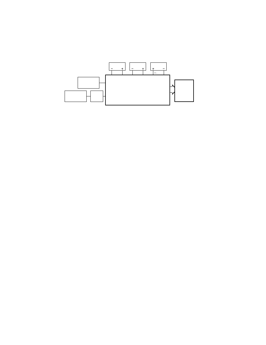
The AD9281 evaluation board is shipped "ready to run."
Power and signal generators should be connected as shown in
Figure 33 Then the user can observe the performance of the Q
channel. If the user wants to observe the I channel, then he
SYNTHESIZER
20MHz
2Vp-p
+5V
DSP
EQUIPMENT
ANTI-
ALIAS
FILTER
+3V
+3V
SYNTHESIZER
1MHz
1Vp-p
AGND
AVDD
DGND1 DVDD DGND2 DRVDD
P1
CLOCK
Q IN
AD9281
Figure 33. Evaluation Board Connections
should install a jumper at JP22 Pins 1 and 2. If the user wants to
toggle between I and Q channels, then a CMOS level pulse train
should be applied to the "strobe" jack after appropriate jumper
connections.
AD9281
15
REV. E
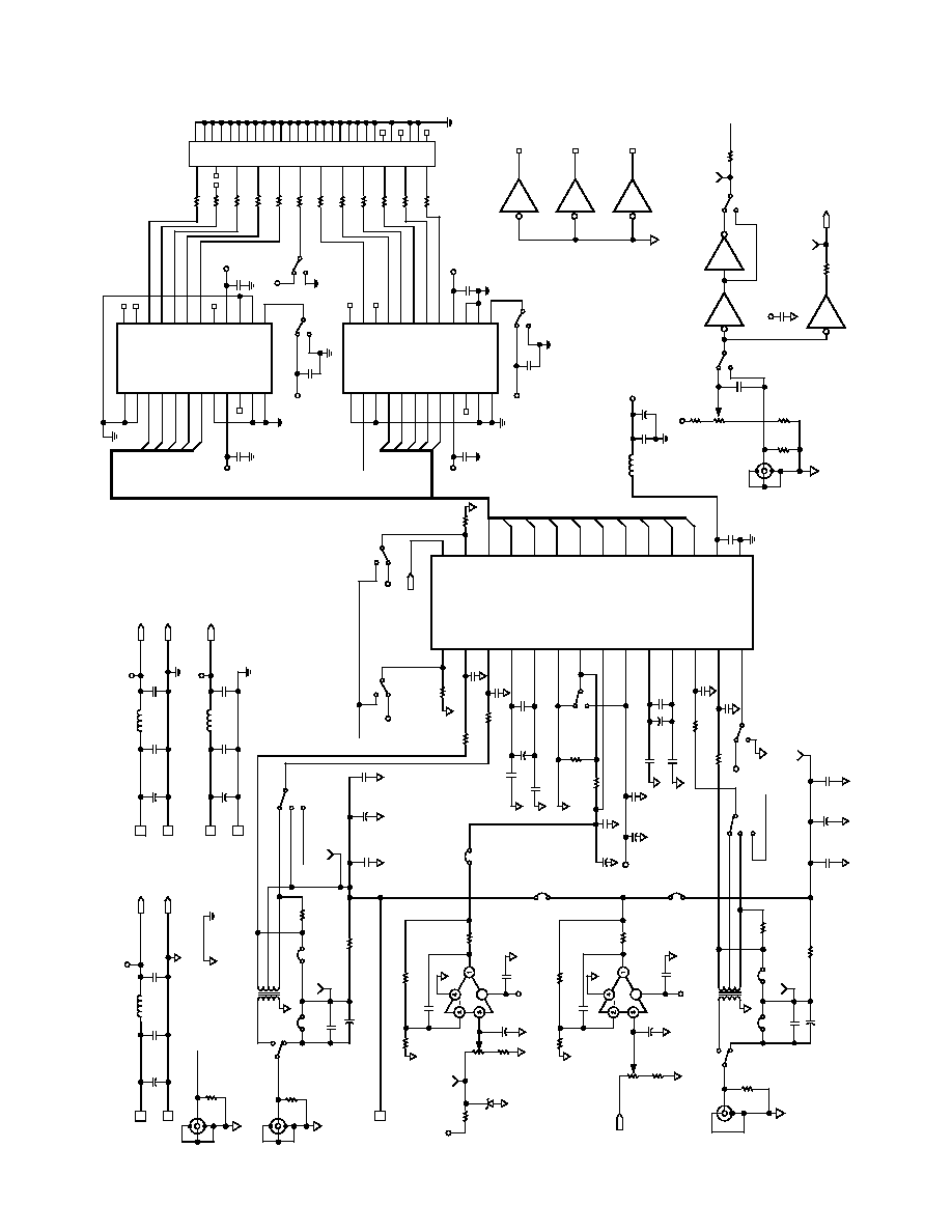
9201EB
R50
R51
C14
C24
R52
R53
C20
C22
C50
C51
C29
C52
C53
C14
C17
C23
C27
+C5
+C36
C35
C55
C4
C54
(NOT TO SCALE)
REV
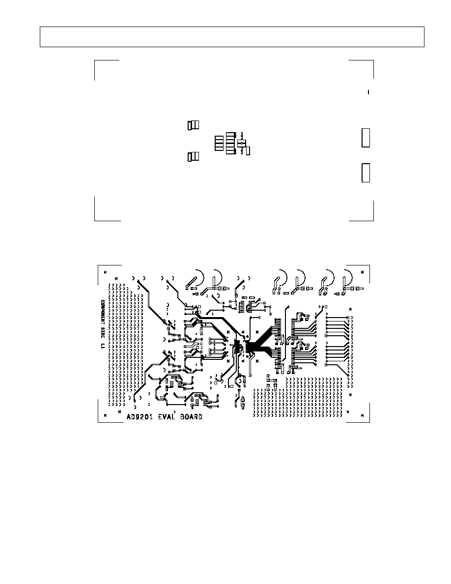
Figure 34. Evaluation Board Solder-Side Silkscreen
(NOT TO SCALE)
Figure 35. Evaluation Board Component-Side Layout
AD9281
16
REV. E
(NOT TO SCALE)
Figure 36. Evaluation Board Ground Plane Layout
(NOT TO SCALE)
Figure 37. Evaluation Board Solder-Side Layout
AD9281
17
REV. E
R14
(NOT TO SCALE)
AGND
R37
R13
R11
JP21
AVDD
J1
J5
BJ2
BJ1
C42
L2
C40
R38
J6
C38
C41
+
JP22
R1
R4
R31
R33
R32
JP13
4
TP2
TP1
C15
+
+
C25
4
TP5
JP14
TP6
T1
JP3
R2
C3
JP10
T2
C1 JP2 JP1
J3
R34
C34
JP7
JP9
R40
R35
C37
JP12JP11
C31
+
AGND
J4
R30
R23
R12
R8
TP3
D1
C32
C21
R9
V6
C12
+
C11
V3
C8
R16
R17
R24
JP6
R6
R7
JP5
V4
JP4
R10
R18
+
C19
C24 +
DGND
L5
C30
C49 +
C9
C10
C2
V2
C13
C6
V1
DBVDD
RN2
JP20
RN1
P1
JP17
C47
L4
BJ5
C48
+ C46
C7
JP19
R36
+ C43
L3
C44
BJ6
BJ4
BJ3
C45
TP4
JP16
V8
TP7
JP15
C33
R39
I_IN
STROBE
AGND
AVDD
CLOCK
DGND1
DVDD
DGND2 DBVDD
Q_IN
Figure 38. Evaluation Board Component-Side Silkscreen
(NOT TO SCALE)
Figure 39. Evaluation Board Power Plane Layout
AD9281
18
REV. E
Figure 40. Evaluation Board
STROBE
AVDD
15
16
17
18
19
20
21
22
23
24
25
26
27
28
AVDD
8
AD822
+
U3
ADJ_REF
AVDD
8
AD822
+
U6
1
J3
1
1
AVDD
1
1
DVDD
1
1
DRVDD
B
B
B
B
B
B
B
B
VCCB
NC1
OE
GND1
A
A
A
A
A
A
A
A
VCCA
T/R
GND2
GND3
U1
C2
0.1
F
16
15
21
20
19
18
17
14
24
23
22
13
D5
D6
D7
D8
D9
DVDD
74LVXC4245
B
B
B
D0
D1
D2
D3
D4
VCCB
NC1
OE
GND1
A
A
A
A
A
A
A
A
VCCA
T/R
GND2
GND3
U2
C9
0.1
F
19
20
21
20
18
17
16
14
24
23
22
13
D0
D1
D2
D3
DVDD
1
3
2
JP16
HDR3
1
3
2
JP15
HDR3
74AHC14DW
74AHC14DW
74AHC14DW
AVDD
U8A
U8B
U8C
C38
0.1
F
1
2
3
4
5
6
DUTCLK
R39
R-S 50
TP7
CON1
TP4
CON1
R-S TBD
R36
CLK0
C33
0.1
F
AVDD
R31
500
R32
POT_2k
R33
500
R38
R-S
50
ADC_CLK
J6
BNC
74LVXC4245
D4
DRVDD
5
4
3
6
7
8
9
10
1
2
11
12
BCLK0
BD0
BD1
BD2
BD3
BD4
BD5
BD7
BD8
BD9
BD6
8
9
3
4
5
6
7
10
1
2
11
12
DRVDD
SLEEP
INA-1
INB-1
REFT-1
REFB-1
AVSS
REFSENSE
VREF
AVDD
REFB-Q
REFT-Q
INB-Q
INA-Q
CHIP-SELECT
DUTCLK
SELECT
D9
D8
D7
D6
D5
D4
D3
D2
D1
D0
DVDD
DVSS
TESTCHIP
14
13
12
11
10
9
8
7
6
5
4
3
D4
D8
D7
D6
D5
D4
D3
D2
D1
D0
D9
31
30
4
2
29
28
3
6
26
24
22
8
10
12
20
25
18
27
16
32
14
34
33
40
39
36
38
37
13
11
9
7
5
1
33
23
21
19
17
15
P1
DRVDD
1
3
2
JP17
HDR3
RESISTOR
7PACK
1
2
3
4
5
6
1
2
3
4
5
6
14
13
12
11
10
9
14
13
12
11
10
9
CLK
OUT
CON40
74AHC14DW
U8F
13
12
74AHC14DW
U8E
11
10
74AHC14DW
U8D
9
8
C10
0.1
F
1
2
3
JP20
HDR3
1
3
2
JP19
HDR3
C7
0.1
F
C6
0.1
F
CLK0
C13
0.1
F
DUTDATA
[0...9]
DGND
DVDD
L3
FERRITE BEAD
C45
CAP_NP
C44
CAP_NP
C43
10_10V
DVDD
L4
FERRITE BEAD
C48
CAP_NP
C47
CAP_NP
C46
10_10V
DRVDD
DRVDD
BJ3
BANA
BJ4
BANA
BJ5
BANA
BJ6
BANA
AVDD
AVDD VCC
L2
FERRITE BEAD
C42
CAP_NP
C41
CAP_NP
C40
10_10V
J5
BNC
STROBE
R37
R-S 49.9
RN1A
RN1B
RN1C
RN1D
RN1E
RN1F
RN2A
RN2B
RN2C
RN2D
RN2E
RN2F
J1
BNC
CH1IN
R2
R-S 50
2
3
1
HDR3
JP3
T1
TRANSFORMER
CT
1
2
3
4
6
PS
JP2
JUMPER
JP2
JUMPER
C1
0.1
F
C3
10_6V3
TP1
CON1
R1
R-S TBD
TP2
CON1
DCIN1
AGND
R_VREF
1
2
3
4
JP13
HDR3
C54
1000pF
C5
10_6V3
C4
0.1
R4
R-S 100
MIDSCALE_IN
AD9201/ AD9281
NOT TO SCALE
DRVDD
D[0...9]
DRVDD
C29
CAP_NP
L5
FERRITE_BEAD
DVDD
C53
10pF
C52
10pF
C23
0.1
F
C25
CAP_P
C26
CAP_NP
C27 0.1
F
R52
10
R53
10
1
3
2
JP6
HDR3
AVDD
INA-Q
INB-Q
2
3
JP14
HDR4
1
4
R_VREF
TP6
CON1
C55
1000pF
C36
10_6V3
C35
0.1
F
R35
R-S 1
TP5
CON1
JP11
JUMPER
J4
BNC
JUMPER
C34 0.1
F
C37
10_6V3
1
2
3
4
6
PS
T2
TRANSFORMER CT
R40
R-S 100
3
1
2
JP10
HDR3
R34
R-S 50
CHOIN
JP12
R30
1.5k
R23
POT_10k
C31
10_6V3
C32 0.1
F
R24
R-S 22
R17
15k
R16
5k
C21
CAP_NP
ADJ_REF
D1
R8
5.49k
DIODE_ZENER
R9
POT_10k
R12
1.5k
C12
0.1k
C11
10_6V3
R10
R-S 10
C8
CAP_NP
R7
15k
R6
5k
JP5
JUMPER
JP7
JUMPER
JP9
JUMPER
C24
10_10V
C19
10_10V
C20
0.1k
C22
0.1k
R18
R-S TBD
R14
R-S TBD
1
2
3
JP4
C16
CAP_NP
C15
CAP_P
C14
0.1
F
C17
0.1
F
C50
10pF
C51
10pF
R51
10
R50
10
R11
1k
DUTCLK
1
2
3
JP22
AVDD
HDR3
3
1
2
HDR3
R13
1k
C30
CAP_NP
C49
10_10V
U4
TP3
CON1
APWRIN
GND
BJ1
BANA
BJ2
BANA
DPWRIN
DPWRIN
INA-1
INB-1
MIDSCALE_I
JP21
VREF
DCINO
AVDD
AVDD
R_VREF
AD9281
19
REV. E
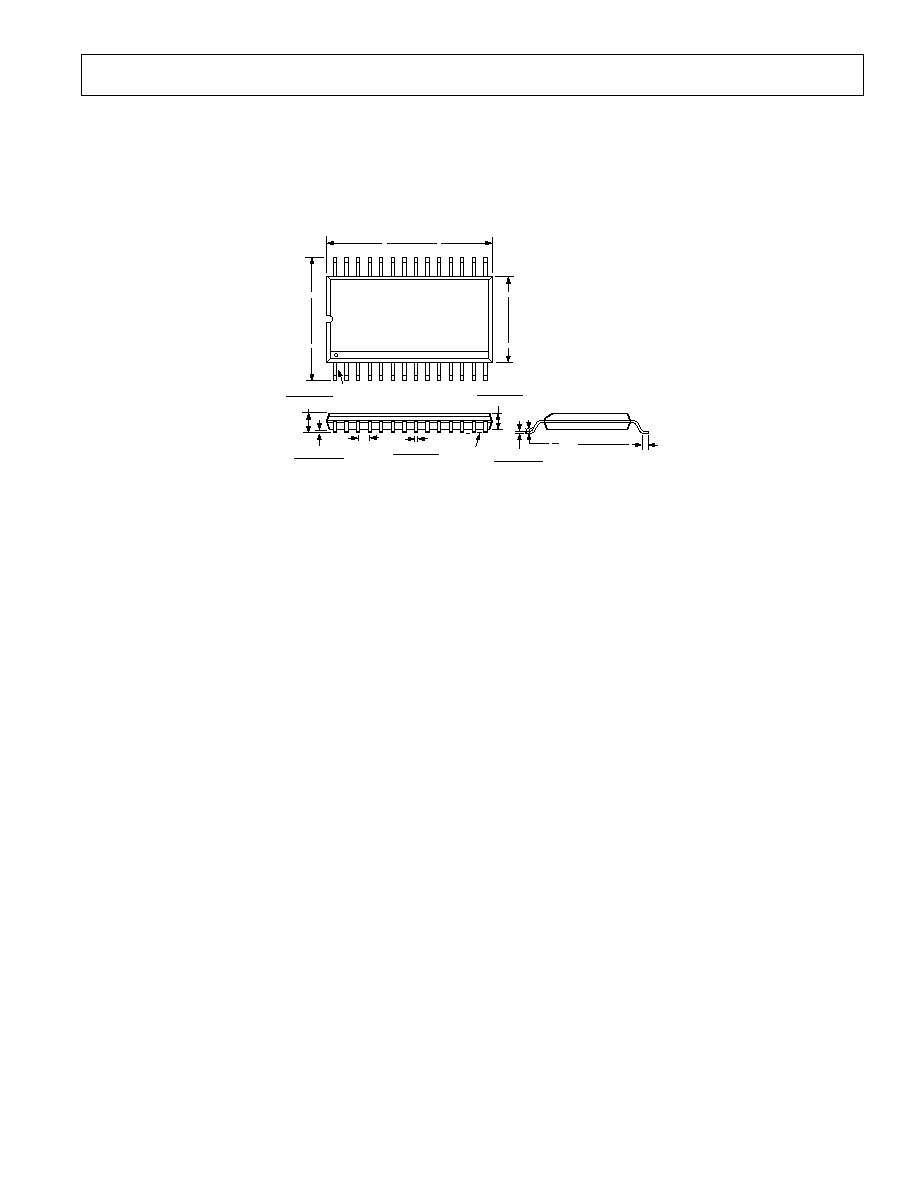
OUTLINE DIMENSIONS
Dimensions shown in inches and (mm).
28-Lead Shrink Small Outline Package (SSOP)
(RS-28)
28
15
14
1
0.407 (10.34)
0.397 (10.08)
0.311 (7.9)
0.301 (7.64)
0.212 (5.38)
0.205 (5.21)
PIN 1
SEATING
PLANE
0.008 (0.203)
0.002 (0.050)
0.07 (1.79)
0.066 (1.67)
0.0256
(0.65)
BSC
0.078 (1.98)
0.068 (1.73)
0.015 (0.38)
0.010 (0.25)
0.009 (0.229)
0.005 (0.127)
0.03 (0.762)
0.022 (0.558)
8°
0°
C3117e08/99
PRINTED IN U.S.A.