 | –≠–ª–µ–∫—Ç—Ä–æ–Ω–Ω—ã–π –∫–æ–º–ø–æ–Ω–µ–Ω—Ç: AD9621AR | –°–∫–∞—á–∞—Ç—å:  PDF PDF  ZIP ZIP |

REV. 0
Information furnished by Analog Devices is believed to be accurate and
reliable. However, no responsibility is assumed by Analog Devices for its
use, nor for any infringements of patents or other rights of third parties
which may result from its use. No license is granted by implication or
otherwise under any patent or patent rights of Analog Devices.
a
AD9621*
One Technology Way, P.O. Box 9106, Norwood, MA 02062-9106, U.S.A.
Tel: 617/329-4700
Fax: 617/326-8703
CONNECTION DIAGRAM
1
2
3
4
8
7
6
5
AD9621
NC #
≠INPUT
+INPUT
≠V
S
NC #
+V
S
OUTPUT
NC
# OPTIONAL CAPACITOR CB CONNECTED HERE
DECREASES SETTLING TIME
FEATURES
350 MHz Small Signal Bandwidth
130 MHz Large Signal BW (4 V p-p)
High Slew Rate: 1200 V/ s
Fast Settling: 11 ns to 0.01%/7 ns to 0.1%
3 V Supply Operation
APPLICATIONS
ADC Input Driver
Differential Amplifiers
IF/RF Amplifiers
Pulse Amplifiers
Professional Video
DAC Current-to-Voltage
Baseband and Video Communications
Pin Diode Receivers
Active Filters/lntegrators/Log Amps
GENERAL DESCRIPTION
The AD9621 is one of a family of very high speed and wide
bandwidth amplifiers utilizing a voltage feedback architecture.
These amplifiers define a new level of performance for voltage
feedback amplifiers, especially in the categories of large signal
bandwidth, slew rate, settling, and low noise.
Proprietary design architectures have resulted in an amplifier
family that combines the most attractive attributes of both cur-
rent feedback and voltage feedback amplifiers. The AD9621 ex-
hibits extraordinarily accurate and fast pulse response
characteristics (7 ns settling to 0.1%) as well as extremely wide
small and large signal bandwidth previously found only in cur-
rent feedback amplifiers. When combined with balanced high
impedance inputs and low input noise current more common to
voltage feedback architectures, the AD9621 offers performance
not previously available in a monolithic operational amplifier.
*Protected by U.S. Patent 5,150,074 and others pending.
Other members of the AD962X amplifier family are the
AD9622 (G = +2), AD9623 (G = +4), and the AD9624
(G = +6). A separate data sheet is available from Analog De-
vices for each model. Each generic device has been designed for
a different minimum stable gain setting, allowing users flexibility
in optimizing system performance. Dynamic performance speci-
fications such as slew rate, settling time, and distortion vary
from model to model. The table below summarizes key perfor-
mance attributes for the AD962X family and can be used as a
selection guide.
The AD9621 is offered in industrial and military temperature
ranges. Industrial versions are available in plastic DIP, SOIC,
and cerdip; MIL versions are packaged in cerdips.
PRODUCT HIGHLIGHTS
1. Wide Large Signal Bandwidth
2. High Slew Rate
3. Fast Settling
4. Output Short-Circuit Protected
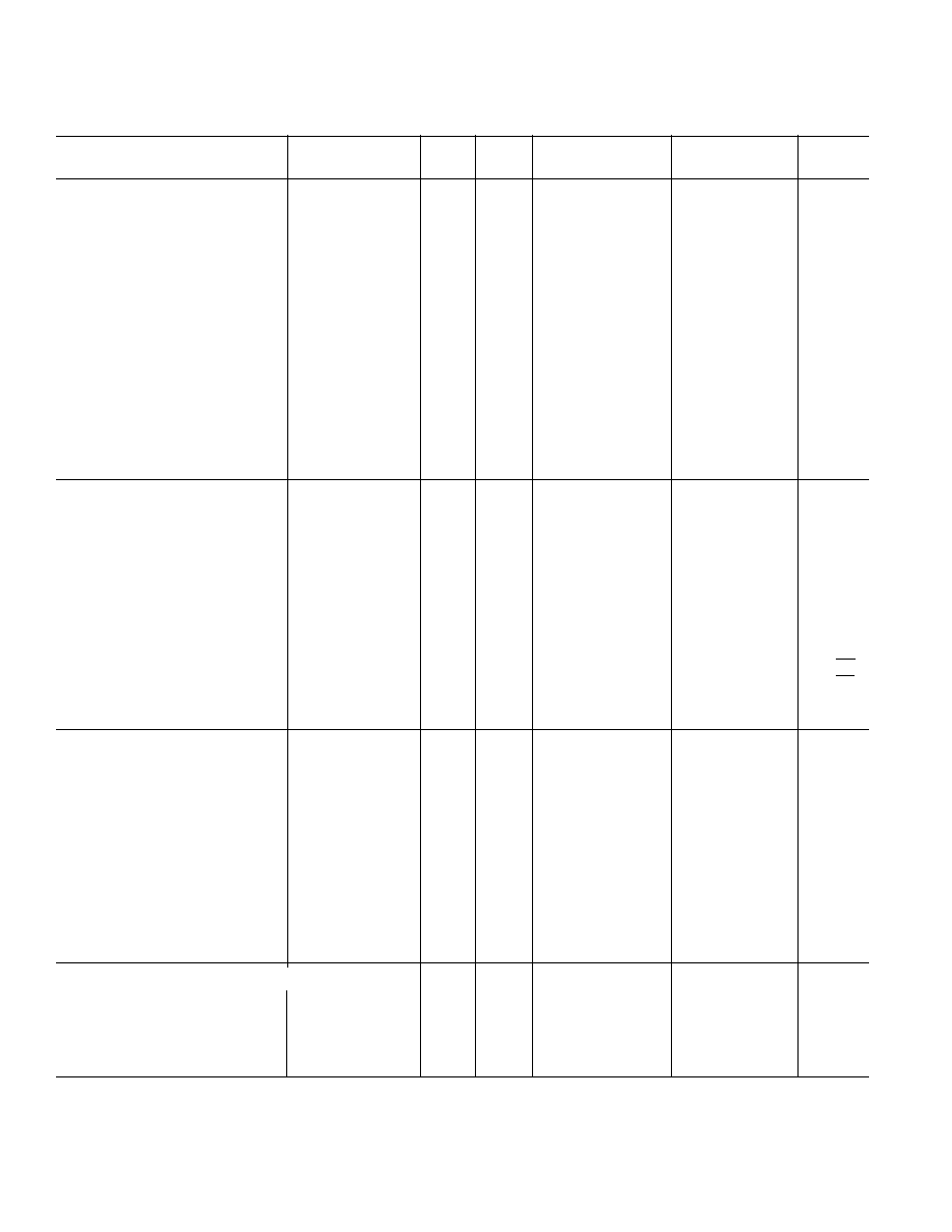
Parameter
AD9621
AD9622
AD9623
AD9624
Units
Minimum Stable Gain
+1
+2
+4
+6
V/V
Harmonic Distortion (20 MHz)
≠52
≠66
≠64
≠66
dB
Large Signal Bandwidth (4 V p-p)
130
160
190
200
MHz
SSBW (0.5 V p-p)
350
220
270
300
MHz
Slew Rate
1200
1500
2100
2200
V/
µ
s
Rise/Fall Time (0.5 V Step)
2.4
1.7
1.6
1.5
ns
Settling Time (to 0.1%/0.01%)
7/11
8/14
8/14
8/14
ns
Input Noise (0.1 MHz ≠ 200 MHz)
80
49
36
32
µ
V rms
Wideband Voltage
Feedback Amplifier
AD9621≠SPECIFICATIONS
DC ELECTRICAL CHARACTERISTICS
Test
AD9621AN/AQ/AR
AD9621SQ
Parameter
Conditions
Temp
Level
Min
Typ
Max
Min
Typ
Max
Units
DC SPECIFICATIONS
1
Input Offset Voltage
+25
∞
C
I
≠12
±
2
+12
≠12
±
2
+12
mV
Full
VI
≠15
+15
≠15
+15
mV
Input Bias Current
+25
∞
C
I
7
16
7
16
µ
A
Full
VI
≠20
+20
≠20
+20
µ
A
Input Bias Current TC
Full
V
35
35
nA/
∞
C
Input Offset Current
+25
∞
C
I
≠2.0
±
0.3
+2.0
≠2.0
+2.0
µ
A
Full
VI
≠3.0
+3.0
≠3.0
+3.0
µ
A
Offset Current TC
Full
V
2.5
2.5
nA/
∞
C
Input Resistance
+25
∞
C
V
500
500
k
Input Capacitance
+25
∞
C
V
1.2
1.2
pF
Common-Mode Range
Full
VI
±
3.0
±
3.4
±
3.0
±
3.4
V
Common-Mode Rejection Ratio
V
CM
= 1 V
+25
∞
C
I
46
49
46
49
dB
Open Loop Gain
V
OUT
=
±
2 V p-p
+25
∞
C
V
56
56
dB
Output Voltage Range
Full
VI
±
3.0
±
3.4
±
3.0
±
3.4
V
Output Current
Full
VI
60
70
60
70
mA
Output Resistance
+25
∞
C
V
0.3
0.3
FREQUENCY DOMAIN
Bandwidth (≠3 dB)
Small Signal
V
OUT
0.4 V p-p
Full
II
230
350
230
350
MHz
Large Signal
V
OUT
4.0 V p-p
Full
V
130
130
MHz
Amplitude of Peaking
Full Spectrum
Full
II
0.1
1.2
0.1
1.2
dB
Amplitude of Roll-off
100 MHz
Full
II
0
0.6
0
0.6
dB
Phase Nonlinearity
DC to 100 MHz
+25
∞
C
V
1.1
1.1
Degree
2nd Harmonic Distortion
2 V p-p; 20 MHz
Full
II
≠55
≠44
≠55
≠44
dBc
3rd Harmonic Distortion
2 V p-p; 20 MHz
Full
II
≠52
≠43
≠52
≠43
dBc
Common-Mode Rejection Mode
@ 20 MHz
+25
∞
C
V
+28
+28
dB
Spectral Input Noise Voltage
1 to 200 MHz
+25
∞
C
V
5.6
5.6
nV/
Hz
Spectral Input Noise Current
1 to 200 MHz
+25
∞
C
V
3.6
3.6
pA/
Hz
Average Equivalent Integrated
Input Noise Voltage
0.1 to 200 MHz
+25
∞
C
V
80
80
µ
V rms
TIME DOMAIN
Slew Rate
V
OUT
= 5 V Step
Full
IV
850
1200
850
1200
V/
µ
s
Rise/Fall Time
V
OUT
= 0.5 V Step
+25
∞
C
V
2.4
2.4
ns
V
OUT
= 5 V Step
Full
IV
4.8
7
4.8
7
ns
Overshoot
V
OUT
= 2 V Step
Full
IV
0
15
0
15
%
Settling Time
To 0.1%
V
OUT
= 2 V Step
+25
∞
C
V
7
7
ns
To 0.01%
V
OUT
= 2 V Step
Full
IV
11
15
11
15
ns
To 0.1%
2
V
OUT
= 4 V Step
+25
∞
C
V
9
9
ns
T0 0.01
2
V
OUT
= 4 V Step
+25
∞
C
V
13
13
ns
Overdrive Recovery
1.5x to
±
2 mV
+25
∞
C
V
50
50
ns
Differential Gain (4.3 MHz)
R
L
= 150
+25
∞
C
V
0.01
0.01
%
Differential Phase (4.3 MHz)
R
L
= 150
+25
∞
C
V
<0.01
<0.01
Degree
POWER SUPPLY REQUIREMENTS
1
Supply Voltage (
±
V
S
)
Full
IV
3.0
5.0
5.5
3.0
5.0
5.5
V
Quiescent Current
+I
S
+V
S
= +5 V
Full
VI
23
29
23
29
mA
≠I
S
≠V
S
= ≠5 V
Full
VI
23
29
23
29
mA
Power Supply Rejection Ratio
V
S
= 0.5 V
+25
∞
C
I
54
66
54
66
dB
NOTES
1
Measured at A
V
= 21.
2
Measured with a 0.001
µ
F C
B
capacitor connected across Pins 1 and 8.
Specifications subject to change without notice.
REV. 0
≠2≠
( V
S
= 5 V, R
LOAD
= 100
; A
V
= 1, unless otherwise noted)

AD9621
REV. 0
≠3≠
ABSOLUTE MAXIMUM RATINGS
1
Supply Voltages (
±
V
S
) . . . . . . . . . . . . . . . . . . . . . . . . . . .
±
6 V
Common-Mode Input Voltage . . . . . . . . . . . . . . . . . . . . . .
±
V
S
Differential Input Voltage . . . . . . . . . . . . . . . . . . . . . . . . . . 6 V
Continuous Output Current
2
. . . . . . . . . . . . . . . . . . . . . 90 mA
Operating Temperature Ranges
AN, AQ, AR . . . . . . . . . . . . . . . . . . . . . . . . ≠40
∞
C to +85
∞
C
SQ . . . . . . . . . . . . . . . . . . . . . . . . . . . . . . . ≠55
∞
C to +125
∞
C
Storage Temperature
Ceramic . . . . . . . . . . . . . . . . . . . . . . . . . . . ≠65
∞
C to +150
∞
C
Plastic . . . . . . . . . . . . . . . . . . . . . . . . . . . . ≠65
∞
C to +125
∞
C
Junction Temperature
Ceramic
3
. . . . . . . . . . . . . . . . . . . . . . . . . . . . . . . . . +175
∞
C
Plastic
3
. . . . . . . . . . . . . . . . . . . . . . . . . . . . . . . . . . . +150
∞
C
Lead Soldering Temperature (1 minute)
4
. . . . . . . . . . +220
∞
C
NOTES
1
Absolute maximum ratings are limiting values to be applied individually, and
beyond which the serviceability of the circuit may be impaired. Functional
operability is not necessarily implied. Exposure to absolute maximum rating
conditions for an extended period of time may affect device reliability.
2
Output is short-circuit protected; for maximum reliability, 90 mA continuous
current should not be exceeded.
3
Typical thermal impedances (part soldered onto board; no air flow):
Ceramic DIP:
JA
= 100
∞
C/W;
JC
= 30
∞
C/W
Plastic SOIC:
JA
= 125
∞
C/W;
JC
= 45
∞
C/W
Plastic DIP:
JA
= 90
∞
C/W;
JC
= 45
∞
C/W
4
Temperature shown is for surface mount devices, mounted by vapor phase
soldering. Throughhole devices (ceramic and plastic DIPs) can be soldered at
+300
∞
C for 10 seconds.
ORDERING GUIDE
Temperature
Package
Package
Model
Range
Description
Option
AD9621AN
≠40
∞
C to +85
∞
C
8-Pin Plastic DIP
N-8
AD9621AQ
≠40
∞
C to +85
∞
C
8-Pin Cerdip
Q-8
AD9621AR
≠40
∞
C to +85
∞
C
8-Pin SOIC
R-8
AD9621SQ
≠55
∞
C to +125
∞
C
8-Pin Cerdip
Q-8
EXPLANATION OF TEST LEVELS
Test Level
I
≠ 100% production tested.
II ≠ 100% production tested at +25
∞
C, and sample tested at
specified temperatures. AC testing of "A" grade devices
done on sample basis.
III ≠ Sample tested only.
IV ≠ Parameter is guaranteed by design and characterization
testing.
V
≠ Parameter is a typical value only.
VI ≠ All devices are 100% production tested at +25
∞
C. 100%
production tested at temperature extremes for extended
temperature devices; sample tested at temperature ex-
tremes for commercial/industrial devices.
≠V
S
46.5mm
≠ INPUT
46.5mils
CB≠
CB+
≠INPUT +INPUT
+V
S
OUTPUT
54mils
Chip Layout
THEORY OF OPERATION
The AD9621 is a wide bandwidth, unity gain stable voltage
feedback amplifier. Since its open-loop frequency response fol-
lows the conventional 6 dB/octave roll-off, its gain bandwidth
product is basically constant. Increasing its closed-loop gain re-
sults in a corresponding decrease in small signal bandwidth. The
AD9621 typically maintains a 55 degree unity loop gain phase
margin. This high margin minimizes the effects of signal and
noise peaking.
Feedback Resistor Choice
At minimum stable gain (+1), the AD9621 provides optimum
dynamic performance with R
F
51
. This resistor acts only as
a parasitic suppressor against damped R
F
oscillations that can
occur due to lead (input, feedback) inductance and parasitic ca-
pacitance. For settling accuracy to 0.1% or less, this resistor
should not be required if layout guidelines are closely followed.
This value for R
F
provides the best combination of wide band-
width, low parasitic peaking, and fast settling time.
When the AD9621 is used in the transimpedance (I-to-V)
mode, such as for photo-diode detection, the value for R
F
and
diode capacitance (C
I
) are usually known. See Figure 1. Gener-
ally, the value of R
F
selected will be in the k
range, and a shunt
capacitor (C
F
) across R
F
will be required to maintain good am-
plifier stability. The value of C
F
required to maintain < 1 dB of
peaking can be estimated as:
C
F
[(2
C
I
R
F
-
1)
2
R
F
2
]
1 2
|
R
F
1 k
where
o
is equal to the unity gain bandwidth product of the
amplifier in RAD/sec, and C
I
is the equivalent total input ca-
pacitance at the inverting input. Typically
o
is 700
◊
10
6
RAD/sec (See Open Loop Frequency Response curve).
As an example, choosing R
F
of 10 k
and C
I
of 5 pF, requires
C
F
to be 1.1 pF (Note: C
I
includes both the source and parasitic
circuit capacitance). The bandwidth of the amplifier can be esti-
mated using the C
F
calculated as:
f
3
dB
1.6
2
R
F
C
F
For general voltage gain applications, the amplifier bandwidth
can be estimated as:
f
3
dB
1
+
R
F
R
G
This estimation loses accuracy for gains approaching +2/≠1 or
lower due to the amplifier's damping factor. For these "low
gain" cases, the bandwidth will actually extend beyond the cal-
culated value. See Closed Loop BW plots.
As a rule of thumb, capacitor C
F
will not be required if:
R
F
R
G
(
)
C
I
NG
4
where NG is the Noise Gain (l + R
F
/R
G
) of the circuit. For most
voltage gain applications, this should be the case.
AD9621
REV. 0
≠4≠
phase margin (55
∞
), low noise current (3.6 pA/
Hz
), and slew
rate (1200 V/
µ
s) give higher performance capabilities to these
applications over previous voltage feedback designs.
With a settling time of 11 ns to 0.01% and 7 ns to 0.1%, the de-
vice is an excellent choice for DAC I/V conversion. The same
characteristics, along with low harmonic distortion, make it a
good choice for ADC buffering/amplification. With its superb
linearity at relatively high signal frequencies, it is an ideal driver
for ADCs up to 14 bits.
Layout Considerations
As with all wide bandwidth components, printed circuit layout
is critical to obtain best dynamic performance with the AD9621.
The ground plane in the area of the amplifier and its associated
components should cover as much of the component side of the
board as possible (or first interior layer of a multi layer surface
mount board).
The ground plane should be removed in the area of the inputs
and R
F
and R
G
to minimize stray capacitance at the input. The
same precaution should be used for C
B
, if used. Each power
supply trace should be decoupled close to the package with a
0.1
µ
F ceramic capacitor, plus a 6.8
µ
F tantalum nearby.
All lead lengths for input, output, and feedback resistor should
be kept as short as possible. All gain setting resistors should be
chosen for low values of parasitic capacitance and inductance,
i.e., microwave resistors and/or carbon resistors.
Microstrip techniques should be used for lead lengths in excess
of one inch. Sockets should be avoided if at all possible because
of their high series inductance. If sockets are necessary, indi-
vidual pin sockets such as AMP p/n 6-330808-3 should be used.
These contribute far less stray reactance than molded socket
assemblies.
An evaluation board is available from Analog Devices for a
nominal charge.
Pulse Response
Unlike a traditional voltage feedback amplifier in which slew
speed is dictated by its front end dc quiescent current and gain
bandwidth product, the AD9621 provides "on demand" trans-
conductance current that increases proportionally to the input
"step" signal amplitude. This results in slew speeds (1200 V/
µ
s)
comparable to wideband current feedback designs. This, com-
bined with relatively low input noise current (3.6 pA/
Hz
), gives
the AD9621 the best attributes of both voltage and current feed-
back amplifiers.
Bootstrap Capacitor (C
B
)
In most applications, the C
B
capacitor will not be required.
Under certain conditions, it can be used to further enhance set-
tling time performance.
The C
B
capacitor (0.001
µ
F) connects to the internal high im-
pedance nodes of the amplifier. Using this capacitor will reduce
the large signal (4 V) step output settling time by 3 to 5 ns for
0.05% or greater accuracy. For settling accuracy less than
0.05% or for smaller step sizes, its effect will be less apparent.
Under heavy slew conditions, this capacitor forces the internal
signal (initial step) amplitude to be controlled by the "on"
(slewed) transistor, preventing its complement from completely
turning off. This allows for faster settling time of these internal
nodes and also the output.
In the frequency domain, total (high frequency) distortion will
be approximately the same with or without C
B
. Typically, the
3rd harmonic will be greater than the 2nd without C
B
. This will
be reversed with C
B
in place.
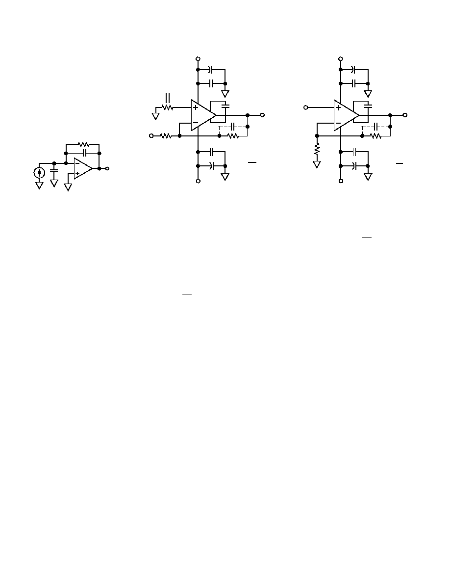
APPLICATIONS
The AD9621 is a voltage feedback amplifier and is well suited
for such applications as photo-detector preamp, active filters,
and log amplifiers. The device's wide bandwidth (350 MHz),
R
F
C
F
C
I
V
OUT
Figure 1. Transimpedance
Configuration
2
3
4
7
6
0.1
µ
F
0.1
µ
F
1
8
6.8
µ
F
R
G
V
IN
6.8
µ
F
+V
S
≠V
S
C
B (OPTIONAL)
C
F
V
OUT
R
F
500
A
V
= 1+
R
F
R
G
Figure 3. Noninverting Gain Connection
Diagram
2
3
4
7
6
0.1
µ
F
0.1
µ
F
1
8
6.8
µ
F
R
F
R
G
R
G
V
IN
6.8
µ
F
+V
S
≠V
S
C
B (OPTIONAL)
C
F
V
OUT
R
F
500
A
V
=
≠R
F
R
G
Figure 2. Inverting Gain Connection
Diagram

AD9621
REV. 0
≠5≠
≠
Typical Performance
(R
L
= 100
; A
V
= +1, unless otherwise noted)
PHASE ≠ Degrees
OPEN-LOOP GAIN ≠ dB
80
60
40
20
0
≠20
0
+15
+30
+45
+60
+75
+90
≠15
≠30
≠45
≠60
FREQUENCY ≠ Hz
10k
100k
1M
10M
100M
600M
GAIN
PHASE
Figure 4. Open-Loop Gain and
Phase
1
10
2
4
6
20
40
60
FREQUENCY ≠ MHz
dBc
≠50
≠60
≠70
≠80
≠90
≠100
≠110
≠120
2nd HARMONIC
RL = 100
2nd HARMONIC
R
L
= 100
2nd HARMONIC
R
L
= 500
3rd HARMONIC
R
L
= 500
V
OUT
= 2V
p-p
3rd HARMONIC
R
L
= 100
Figure 7. Harmonic Distortion
vs. Frequency
+2
0
≠2
≠4
≠6
≠8
MAGNITUDE ≠ dB
PHASE ≠ Degrees
+180
+135
+90
+45
0
≠45
≠90
≠135
≠180
FREQUENCY ≠ MHz
50
100 150
200
250 300 350 400
450 500
R
LOAD
= 500
R
LOAD
= 50
AV = 1
R
F
= 51
Figure 10. Frequency Response
vs. R
LOAD
FREQUENCY ≠ Hz
10
8
6
4
2
1
10
2
10
3
10
4
10
5
10
6
10
8
6
4
2
1
VOLTAGE
CURRENT
NOISE CURRENT ≠ pA
Hz
NOISE VOLTAGE ≠ nV/
Hz
Figure 13. Input Spectral Noise
Density
+2
0
≠2
≠4
≠6
≠8
MAGNITUDE ≠ dB
PHASE ≠ Degrees
+180
+135
+90
+45
0
≠45
≠90
≠135
≠180
FREQUENCY ≠ MHz
50
100
150
200
250 300
350 400 450 500
A
V
= ≠1
A
V
= ≠2
Figure 5. Inverting Frequency
Response
1
100
10
FREQUENCY ≠ MHz
INTERCEPT ≠ +dBm
40
0
20
10
30
50
50
OUT
Figure 8. Third Order Intercept
+0.1
≠0.1
≠0.04
≠0.08
≠0.06
+0.02
≠0.02
0
+0.04
+0.06
+0.08
50
0
40
30
20
10
TIME ≠ ns
SETTLING PERCENTAGE
V
OUT
= 2V STEP
TEST CIRCUIT
100
6pF
Figure 11. Short-Term Settling
Time
SUPPLY VOLTAGE ≠
±
Volts
5.5
5.0
4.5
4.0
3.5
OUTPUT LEVEL ≠
±
Volts
4
3
2
SUPPLY CURRENT ≠ mA
27
23
19
VOLTAGE
CURRENT
Figure 14. Output Level and
Supply Current vs. Supply Voltage
+2
0
≠2
≠4
≠6
≠8
MAGNITUDE ≠ dB
PHASE ≠ Degrees
+180
+135
+90
+45
0
≠45
≠90
≠135
≠180
FREQUENCY ≠ MHz
50
100 150
200 250 300 350
400
450
500
A
V
= 1
A
V
= 2
A
V
= 4
Figure 6. Noninverting Frequency
Response
+20
+45
+70
+25
+30
+35
+40
+50
+55
+60
+65
CMRR
1
10
1G
10M
1M
100k
10k
1k
100
100M
FREQUENCY ≠ Hz
PSRR
POWER SUPPLY AND COMMON
MODE REJECTION RATIOS ≠ dB
Figure 9. CMRR and PSRR vs.
Frequency
100K
1
10K
1K
100
10
TIME ≠ ns
+0.1
≠0.1
≠0.04
≠0.08
≠0.06
+0.02
≠0.02
0
+0.04
+0.06
+0.08
SETTLING PERCENTAGE
V
OUT
= 2V STEP
TEST CIRCUIT
100
6pF
+2V
0
MEASURING
POINT
Figure 12. Long-Term Settling Time
0
50
20
10
30
40
30
18
14
22
26
R
S
≠ Ohms
10
100
10
1
C
LOAD
≠ pF
R
S
t
SETTLING
TO 0.01% ≠ ns
t
SETTLING
51
R
S
1k
C
L
Figure 15. Settling Time vs.
Capacitive Load

AD9621
REV. 0
≠6≠
C1721≠24≠10/92
PRINTED IN U.S.A.
0
2V
≠2V
5ns/DIV
R
LOAD
= 100
V
OUT
= 5V
p-p
INPUT RISE/FALL TIME = 1.6ns
V
OUT
≠0.2V/DIV
Figure 16. Large Signal Pulse
Response
0
0.2V
≠0.2V
5ns/DIV
R
LOAD
= 100
V
OUT
= 0.4V
p-p
INPUT RISE/FALL TIME = 0.3ns
V
OUT
≠40mV/DIV
Figure 17. Small Signal Pulse
Response
50
10
20
30
40
5
1
3
NONINVERTING GAIN
SETTLING TIME ≠ ns
TO 0.01%
R
LOAD
= 100
V
OUT
= 2V
p-p
Figure 18. Settling Time vs.
Noninverting Gain
MECHANICAL INFORMATION
Dimensions shown in inches and (mm).
Cerdip (Suffix Q)
0.015 (0.38)
0.008 (0.20)
0.005 (0.13) MIN
0.055 (1.4) MAX
1
PIN 1
4
5
8
0.310 (7.87)
0.220 (5.59)
0.405 (10.29) MAX
0.200
(5.08)
MAX
SEATING
PLANE
0.023 (0.58)
0.014 (0.36)
0.070 (1.78)
0.030 (0.76)
0.060 (1.52)
0.015 (0.38)
0.150
(3.81)
MIN
0.200 (5.08)
0.125 (3.18)
0.100
(2.54)
BSC
0
∞
TO 15
∞
0.320 (8.13)
0.290 (7.37)
Plastic DIP (Suffix N)
0.240 (6.096)
0.260 (6.604)
4
5
8
1
SEATING
PLANE
0.200
(5.08)
MAX
0.360 (9.144)
0.400 (10.16)
0.016 (0.406)
0.020(0.508)
0.045 (1.143)
0.065 (2.667)
0.100
(2.54)
BSC
0.290 (7.366)
0.310 (7.874)
0.015 (0.381)
0.008 (0.204)
0.120 (3.048)
0.140 (3.556)
0.140
(3.556)
MIN
0
∞
-15
∞
PIN 1
Plastic SOIC (Suffix R)
TOP
VIEW
0.050
(1.27)
TYP
0.196 (5.00)
0.188 (4.75)
0.180 (0.46)
0.014 (0.36)
0.069 (1.75)
0.053 (1.35)
0.244 (6.20)
0.228 (5.80)
0.010 (0.25)
0.004 (0.10)
0.045 (1.15)
0.020 (0.50)
0.015 (0.38)
0.007 (0.18)
0.206 (5.20)
0.181 (4.60)
0.158 (4.00)
0.150 (3.80)