 | –≠–ª–µ–∫—Ç—Ä–æ–Ω–Ω—ã–π –∫–æ–º–ø–æ–Ω–µ–Ω—Ç: AD9761 | –°–∫–∞—á–∞—Ç—å:  PDF PDF  ZIP ZIP |

REV. A
Information furnished by Analog Devices is believed to be accurate and
reliable. However, no responsibility is assumed by Analog Devices for its
use, nor for any infringements of patents or other rights of third parties
which may result from its use. No license is granted by implication or
otherwise under any patent or patent rights of Analog Devices.
a
AD9761
One Technology Way, P.O. Box 9106, Norwood, MA 02062-9106, U.S.A.
Tel: 781/329-4700
World Wide Web Site: http://www.analog.com
Fax: 7817/326-8703
© Analog Devices, Inc., 2000
Dual 10-Bit TxDAC+TM
with 2 Interpolation Filters
FUNCTIONAL BLOCK DIAGRAM
ACOM
REFLO
"I"
DAC
FSADJ
IOUTA
IOUTB
WRITE INPUT
SELECT INPUT
DCOM
DVDD
CLOCK
AD9761
2
LATCH
"I"
REFIO
REFERENCE
COMP1
COMP2
COMP3
BIAS
GENERATOR
QOUTA
QOUTB
2
LATCH
"Q"
MUX
CONTROL
AVDD
DAC DATA
INPUTS
(10 BITS)
SLEEP
"Q"
DAC
FEATURES
Complete 10-Bit, 40 MSPS Dual Transmit DAC
Excellent Gain and Offset Matching
Differential Nonlinearity Error: 0.5 LSB
Effective Number of Bits: 9.5
Signal-to-Noise and Distortion Ratio: 59 dB
Spurious-Free Dynamic Range: 71 dB
2 Interpolation Filters
20 MSPS/Channel Data Rate
Single Supply: +2.7 V to +5.5 V
Low Power Dissipation: 200 mW (+3 V Supply @
40 MSPS)
On-Chip Reference
28-Lead SSOP
PRODUCT DESCRIPTION
The AD9761 is a complete dual channel, high speed, 10-bit
CMOS DAC. The AD9761 has been developed specifically for
use in wide bandwidth communication applications (e.g., spread
spectrum) where digital I and Q information is being processed
during transmit operations. It integrates two 10-bit, 40 MSPS
DACs, dual 2
◊
interpolation filters, a voltage reference, and
digital input interface circuitry. The AD9761 supports a
20 MSPS per channel input data rate that is then interpolated
by 2
◊
up to 40 MSPS before simultaneously updating each
DAC.
The interleaved I and Q input data stream is presented to the
digital interface circuitry, which consists of I and Q latches as well
as some additional control logic. The data is de-interleaved back
into its original I and Q data. An on-chip state machine ensures the
proper pairing of I and Q data. The data output from each latch is
then processed by a 2
◊
digital interpolation filter that eases the
reconstruction filter requirements. The interpolated output of each
filter serves as the input of their respective 10-bit DAC.
The DACs utilize a segmented current source architecture com-
bined with a proprietary switching technique to reduce glitch
energy and to maximize dynamic accuracy. Each DAC provides
differential current output thus supporting single-ended or
differential applications. Both DACs are simultaneously up-
dated and provide a nominal full-scale current of 10 mA. Also,
the full-scale currents between each DAC are matched to within
0.07 dB (i.e., 0.75%), thus eliminating the need for additional
gain calibration circuitry.
The AD9761 is manufactured on an advanced low cost CMOS
process. It operates from a single supply of 2.7 V to 5.5 V and
consumes 200 mW of power. To make the AD9761 complete it
also offers an internal 1.20 V temperature-compensated bandgap
reference.
TxDAC+ is a trademark of Analog Devices, Inc.
PRODUCT HIGHLIGHTS
1. Dual 10-Bit, 40 MSPS DACs: A pair of high performance
40 MSPS DACs optimized for low distortion performance
provide for flexible transmission of I and Q information.
2. 2
◊
Digital Interpolation Filters: Dual matching FIR interpo-
lation filters with 62.5 dB stop band rejection precede each
DAC input thus reducing the DACs' reconstruction filter
requirements.
3. Low Power: Complete CMOS Dual DAC function operates
on a low 200 mW on a single supply from 2.7 V to 5.5 V.
The DAC full-scale current can be reduced for lower power
operation, and a sleep mode is provided for power reduction
during idle periods.
4. On-Chip Voltage Reference: The AD9761 includes a 1.20 V
temperature-compensated bandgap voltage reference.
5. Single 10-Bit Digital Input Bus: The AD9761 features a
flexible digital interface allowing each DAC to be addressed
in a variety of ways including different update rates.
6. Small Package: The AD9761 offers the complete integrated
function in a compact 28-lead SSOP package.
7. Product Family: The AD9761 Dual Transmit DAC has a
pair of Dual Receive ADC companion products, the AD9281
(8 bits) and AD9201 (10 bits).

≠2≠
REV. A
AD9761≠SPECIFICATIONS
DC SPECIFICATIONS
Parameter
Min
Typ
Max
Units
RESOLUTION
10
Bits
DC ACCURACY
1
Integral Linearity Error (INL)
T
A
= +25
∞
C
≠1.75
±
0.5
1.75
LSB
T
MIN
to T
MAX
≠2.75
±
0.7
2.75
LSB
Differential Nonlinearity (DNL)
T
A
= +25
∞
C
≠1
±
0.4
1.25
LSB
T
MIN
to T
MAX
≠1
±
0.5
1.75
LSB
Monotonicity (10 Bit)
GUARANTEED OVER RATED SPECIFICATION TEMPERATURE RANGE
ANALOG OUTPUT
Offset Error
≠0.05
±
0.025
0.05
% of FSR
Offset Matching between DACs
≠0.10
±
0.05
0.10
% of FSR
Gain Error (without Internal Reference)
≠5.5
±
1.0
5.5
% of FSR
Gain Error (with Internal Reference)
≠5.5
±
1.0
5.5
% of FSR
Gain Matching between DACs
≠1.0
±
0.25
1.0
% of FSR
Full-Scale Output Current
2
10
mA
Output Compliance Range
≠1.0
1.25
V
Output Resistance
100
k
Output Capacitance
5
pF
REFERENCE OUTPUT
Reference Voltage
1.14
1.20
1.26
V
Reference Output Current
3
100
nA
REFERENCE INPUT
Input Compliance Range
0.1
1.25
V
Reference Input Resistance
1
M
TEMPERATURE COEFFICIENTS
Unipolar Offset Drift
0
ppm/
∞
C
Gain Drift (without Internal Reference)
±
50
ppm/
∞
C
Gain Drift (with Internal Reference)
±
140
ppm/
∞
C
Gain Matching Drift (Between DACs)
±
25
ppm/
∞
C
Reference Voltage Drift
±
50
ppm/
∞
C
POWER SUPPLY
AVDD
Voltage Range
2.7
5.0
5.5
V
Analog Supply Current (I
AVDD
)
26
35
mA
DVDD
Voltage Range
2.7
5.0
5.5
V
Digital Supply Current at 5 V (I
DVDD
)
4
70
85
mA
Digital Supply Current at 3 V (I
DVDD
)
4
35
mA
Nominal Power Dissipation
5
AVDD and DVDD at 3 V
200
250
mW
AVDD and DVDD at 5 V
500
650
mW
Power Supply Rejection Ratio (PSRR)≠AVDD
≠0.25
0.25
% of FSR/V
Power Supply Rejection Ratio (PSRR)≠DVDD
≠0.02
0.02
% of FSR/V
OPERATING RANGE
≠40
+85
∞
C
NOTES
1
Measured at IOUTA and QOUTA, driving a virtual ground.
2
Nominal full-scale current, I
OUTFS
, is 16
◊
the I
REF
current.
3
Use an external amplifier to drive any external load.
4
Measured at f
CLOCK
= 40 MSPS and f
OUT
= 1 MHz.
5
Measured as unbuffered voltage output into 50
R
LOAD
at IOUTA, IOUTB, QOUTA, and QOUTB, f
CLOCK
= 40 MSPS and f
OUT
= 8 MHz.
Specifications subject to change without notice.
(T
MIN
to T
MAX
, AVDD = +5 V, DVDD = +5 V, I
OUTFS
= 10 mA, unless otherwise noted)
≠3≠
REV. A
AD9761
DYNAMIC SPECIFICATIONS
Parameter
Min
Typ
Max
Units
DYNAMIC PERFORMANCE
Maximum Output Update Rate
40
MSPS
Output Settling Time (t
ST
to 0.025%)
35
ns
Output Propagation Delay (t
PD
)
55
Input Clock Cycles
Glitch Impulse
5
pV-s
Output Rise Time (10% to 90%)
2.5
ns
Output Fall Time (10% to 90%)
2.5
ns
AC LINEARITY TO NYQUIST
Signal-to-Noise and Distortion (SINAD)
f
OUT
= 1 MHz; CLOCK = 40 MSPS
56
59
dB
Effective Number of Bits (ENOBs)
9.0
9.5
Bits
Total Harmonic Distortion (THD)
f
OUT
= 1 MHz; CLOCK = 40 MSPS
≠68
≠58
dB
Spurious-Free Dynamic Range (SFDR)
f
OUT
= 1 MHz; CLOCK = 40 MSPS; 10 MHz Span
59
68
dB
Channel Isolation
f
OUT
= 8 MHz; CLOCK = 40 MSPS; 10 MHz Span
90
dBC
DIGITAL SPECIFICATIONS
Parameter
Min
Typ
Max
Units
DIGITAL INPUTS
Logic "1" Voltage @ DVDD = +5 V
3.5
5
V
Logic "1" Voltage @ DVDD = +3 V
2.4
3
V
Logic "0" Voltage @ DVDD = +5 V
0
1.3
V
Logic "0" Voltage @ DVDD = +3 V
0
0.9
V
Logic "1" Current
≠10
+10
µ
A
Logic "0" Current
≠10
+10
µ
A
Input Capacitance
5
pF
Input Setup Time (t
S
)
3
ns
Input Hold Time (t
H
)
2
ns
CLOCK High
5
ns
CLOCK Low
5
ns
Invalid CLOCK/WRITE Window (t
CINV
)
1
1
5
ns
NOTES
1
t
CINV
is an invalid window of 4 ns duration beginning 1 ns AFTER the rising edge of WRITE in which the rising edge of CLOCK MUST NOT occur.
Specifications subject to change without notice.
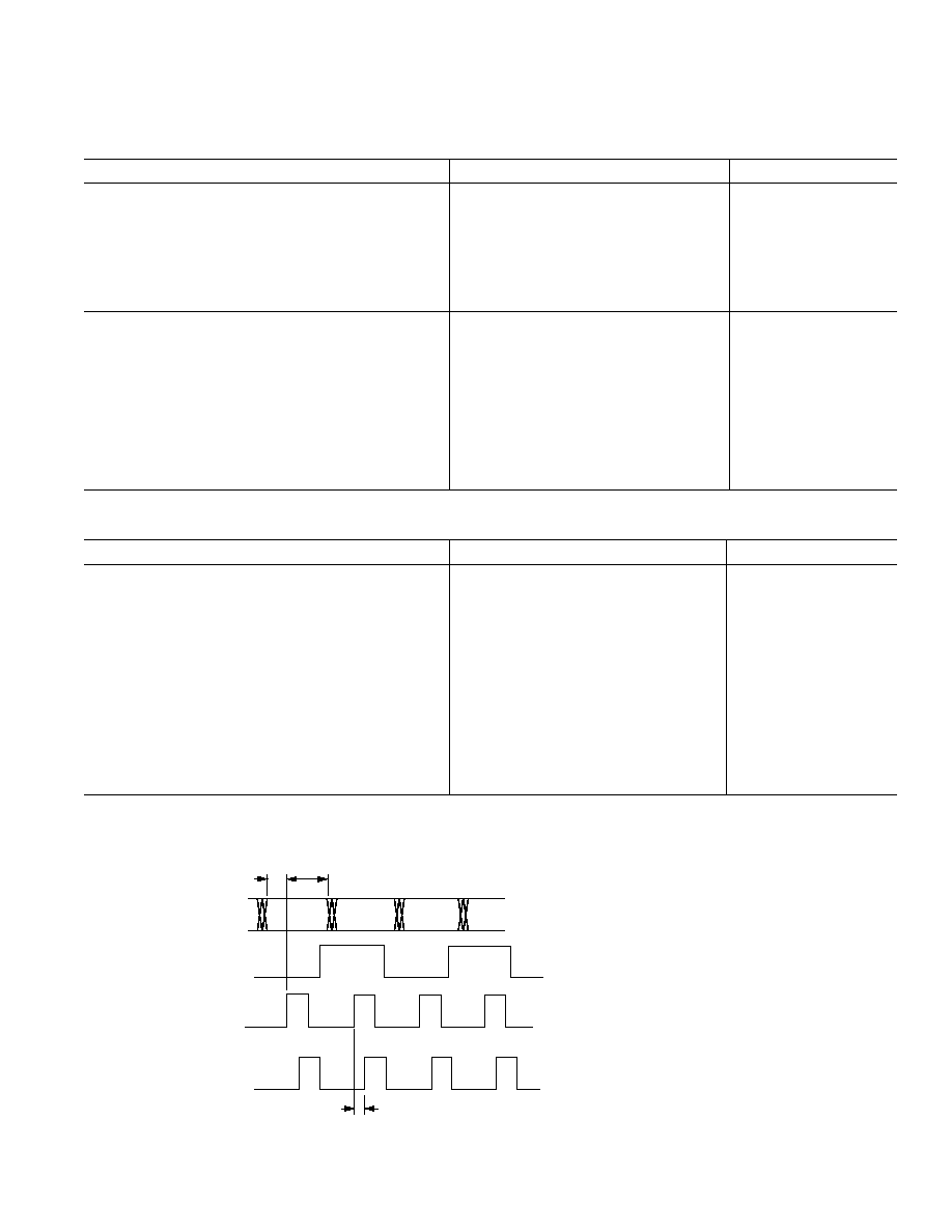
"I" DATA
"Q" DATA
t
CINV
DB9≠DB0
DAC
INPUTS
SELECT
WRITE
CLOCK
t
S
t
H
NOTES: WRITE AND CLOCK CAN BE TIED
TOGETHER. FOR TYPICAL EXAMPLES, REFER
TO DIGITAL INPUTS AND INTERLEAVED INTERFACE
CONSIDERATION SECTION.
Figure 1. Timing Diagram
(T
MIN
to T
MAX
, AVDD = +5 V, DVDD = +5 V, I
OUTFS
= 10 mA, Differential Transformer Coupled Output,
50 Doubly Terminated, unless otherwise noted)
(T
MIN
to T
MAX
, AVDD = +5 V, DVDD = +5 V, I
OUTFS
= 10 mA unless otherwise noted)

AD9761
≠4≠
REV. A
DIGITAL FILTER SPECIFICATIONS
Parameter
Min
Typ
Max
Units
MAXIMUM INPUT CLOCK RATE (f
CLOCK
)
40
MSPS
DIGITAL FILTER CHARACTERISTICS
Passband Width
1
: 0.005 dB
0.2010
f
OUT
/f
CLOCK
Passband Width: 0.01 dB
0.2025
f
OUT
/f
CLOCK
Passband Width: 0.1 dB
0.2105
f
OUT
/f
CLOCK
Passband Width: ≠3 dB
0.239
f
OUT
/f
CLOCK
Linear Phase (FIR Implementation)
Stopband Rejection: 0.3 f
CLOCK
to 0.7 f
CLOCK
≠62.5
dB
Group Delay
2
32
Input Clock Cycles
Impulse Response Duration
3
≠40 dB
28
Input Clock Cycles
≠60 dB
40
Input Clock Cycles
NOTES
1
Excludes SINX/X characteristic of DAC.
2
Defined as the number of data clock cycles between impulse input and peak of output response.
3
55 input clock periods from input to I DAC, 56 to Q DAC. Propagation delay is delay from data input to DAC update.
(T
MIN
to T
MAX
, AVDD = +2.7 V to 5.5 V, DVDD = +2.7 V to 5.5 V, I
OUTFS
= 10 mA unless
otherwise noted)
FREQUENCY RESPONSE ≠ DC to f
CLOCK
/2
OUTPUT ≠ dBFS
0
≠20
≠120
0
0.5
0.1
0.2
0.3
0.4
≠40
≠60
≠80
≠100
Figure 2a. FIR Filter Frequency Response
TIME ≠ Samples
1
0
0
40
5
10
15
20
25
30
35
0.9
0.6
0.4
0.2
0.1
0.8
0.7
0.5
0.3
≠0.1
≠0.2
≠0.3
NORMALIZED OUTPUT
Figure 2b. FIR Filter Impulse Response
Table I. Integer Filter Coefficients for 43-Tap Halfband
FIR Filter
Lower Coefficient
Upper Coefficient
Integer Value
H(1)
H(43)
1
H(2)
H(42)
0
H(3)
H(41)
≠3
H(4)
H(40)
0
H(5)
H(39)
8
H(6)
H(38)
0
H(7)
H(37)
≠16
H(8)
H(36)
0
H(9)
H(35)
29
H(10)
H(34)
0
H(11)
H(33)
≠50
H(12)
H(32)
0
H(13)
H(31)
81
H(14)
H(30)
0
H(15)
H(29)
≠131
H(16)
H(28)
0
H(17)
H(27)
216
H(18)
H(26)
0
H(19)
H(25)
≠400
H(20)
H(24)
0
H(21)
H(23)
1264
H(22)
1998

AD9761
≠5≠
REV. A
ORDERING GUIDE
Package
Package
Model
Description
Option
AD9761ARS 28-Lead Shrink Small Outline (SSOP) RS-28
AD9761-EB
Evaluation Board
CAUTION
ESD (electrostatic discharge) sensitive device. Electrostatic charges as high as 4000 V readily
accumulate on the human body and test equipment and can discharge without detection.
Although the AD9761 features proprietary ESD protection circuitry, permanent damage may
occur on devices subjected to high energy electrostatic discharges. Therefore, proper ESD
precautions are recommended to avoid performance degradation or loss of functionality.
ABSOLUTE MAXIMUM RATINGS*
With
Parameter
Respect to
Min
Max
Units
AVDD
ACOM
≠0.3
+6.5
V
DVDD
DCOM
≠0.3
+6.5
V
ACOM
DCOM
≠0.3
+0.3
V
AVDD
DVDD
≠6.5
+6.5
V
CLOCK, WRITE
DCOM
≠0.3
DVDD+0.3
V
SELECT, SLEEP
DCOM
≠0.3
DVDD+0.3
V
Digital Inputs
DCOM
≠0.3
DVDD+0.3
V
IOUTA, IOUTB
ACOM
≠1.0
AVDD+0.3
V
QOUTA, QOUTB
ACOM
≠1.0
AVDD+0.3
V
COMP1, COMP2
ACOM
≠0.3
AVDD+0.3
V
COMP3
ACOM
≠0.3
AVDD+0.3
V
REFIO, FSADJ
ACOM
≠0.3
AVDD+0.3
V
REFLO
ACOM
≠0.3
+0.3
V
Junction Temperature
+150
∞
C
Storage Temperature
≠65
+150
∞
C
Lead Temperature (10 sec)
+300
∞
C
*This is a stress rating only; functional operation of the device at these or any other conditions above
those listed in the operational sections of this specification is not implied. Exposure to absolute
maximum rating conditions for extended periods may affect device reliability.
THERMAL CHARACTERISTICS
Thermal Resistance
28-Lead SSOP
JA
= 109
∞
C/W
Figure 3. Basic AC Characterization Test Setup
WARNING!
ESD SENSITIVE DEVICE
COMP1
"I"
DAC
FSADJ
IOUTA
IOUTB
WRITE
SELECT
COMP3
AVDD
AVSS
AD9761
2x
LATCH
"I"
REFLO
"Q"
DAC
QOUTA
QOUTB
2x
LATCH
"Q"
MUX
CONTROL
COMP2
DB9≠DB0
SLEEP
CLOCK
REFIO
100
50
20pF
50
20pF
DIGITAL
DATA
TEKTRONIX
AWG-2021
CLOCK
OUT
MARKER 1
RETIMED
CLOCK
OUTPUT
*
LE CROY 9210
PULSE GENERATOR
*
AWG2021 CLOCK RETIMED SUCH THAT DIGITAL DATA
TRANSITIONS ON FALLING EDGE OF 50% DUTY CYCLE CLOCK.
MINI-CIRCUITS
T1-1T
R
SET
2k
0.1 F
TO HP3589A
SPECTRUM/NETWORK
ANALYZER
50 INPUT
100
50
20pF
50
20pF
MINI-CIRCUITS
T1-1T
TO HP3589A
SPECTRUM/NETWORK
ANALYZER
50 INPUT
0.1 F
0.1 F
0.1 F
DVDD DCOM
+2.7V TO
5.5V
+2.7V TO
5.5V

AD9761
≠6≠
REV. A
PIN FUNCTION DESCRIPTIONS
Pin No.
Name
Description
1
DB9
Most Significant Data Bit (MSB).
2≠9
DB8≠DB1
Data Bits 1-8.
10
DB0
Least Significant Data Bit (LSB).
11
CLOCK
Clock Input. Both DACs' outputs updated on positive edge of clock and digital filters read respective
input registers.
12
WRITE
Write input. DAC input registers latched on positive edge of write.
13
SELECT
Select Input. Select high routes input data to I DAC, select low routes data to Q DAC.
14
DVDD
Digital Supply Voltage (+2.7 V to +5.5 V).
15
DCOM
Digital Common.
16
COMP3
Internal Bias Node for Switch Driver Circuitry. Decouple to ACOM with 0.1
µ
F capacitor.
17
QOUTA
Q DAC Current Output. Full-scale current when all data bits are 1s.
18
QOUTB
Q DAC Complementary Current Output. Full-scale current when all data bits are 0s.
19
REFLO
Reference Ground when Internal 1.2 V Reference Used. Connect to AVDD to disable internal
reference.
20
REFIO
Reference Input/Output. Serves as reference input when internal reference disabled. Serves as 1.2 V
reference output when internal reference activated. Requires 0.1
µ
F capacitor to ACOM when inter-
nal reference activated.
21
FSADJ
Full-Scale Current Output Adjust. Resistance to ACOM sets full-scale output current.
22
COMP2
Bandwidth/Noise Reduction Node. Add 0.1
µ
F to AVDD for optimum performance.
23
AVDD
Analog Supply Voltage (+2.7 V to +5.5 V).
24
ACOM
Analog Common.
25
IOUTB
I DAC Complementary Current Output. Full-scale current when all data bits are 0s.
26
IOUTA
I DAC Current Output. Full-scale current when all data bits are 1s.
27
COMP1
Internal Bias Node for Switch Driver Circuitry. Decouple to AGND with 0.1
µ
F capacitor.
28
RESET/SLEEP
Power-Down control input if asserted for four clock cycles or longer. Reset control input if asserted
for less than four clock cycles. Active high. Connect to DCOM if not used. Refer to RESET/SLEEP
section.
PIN CONFIGURATION
14
13
12
11
17
16
15
20
19
18
10
9
8
1
2
3
4
7
6
5
TOP VIEW
(Not to Scale)
28
27
26
25
24
23
22
21
AD9761
(MSB) DB9
IOUTB
IOUTA
COMP1
RESET/SLEEP
DB8
DB7
DB6
COMP2
AVDD
ACOM
DB5
DB4
DB3
DB2
DB1
(LSB) DB0
REFLO
REFIO
FSADJ
CLOCK
WRITE
SELECT
DVDD
QOUTB
DCOM
COMP3
QOUTA

AD9761
≠7≠
REV. A
DEFINITIONS OF SPECIFICATIONS
Linearity Error (Also Called Integral Nonlinearity or INL)
Linearity error is defined as the maximum deviation of the
actual analog output from the ideal output, determined by a
straight line drawn from zero to full scale.
Differential Nonlinearity (or DNL)
DNL is the measure of the variation in analog value, normalized
to full scale, associated with a 1 LSB change in digital input
code.
Monotonicity
A D/A converter is monotonic if the output either increases or
remains constant as the digital input increases.
Offset Error
The deviation of the output current from the ideal of zero is
called offset error. For IOUTA, 0 mA output is expected when
the inputs are all 0s. For IOUTB, 0 mA output is expected
when all inputs are set to 1s.
Gain Error
The difference between the actual and ideal output span. The
actual span is determined by the output when all inputs are set
to 1s minus the output when all inputs are set to 0s.
Output Compliance Range
The range of allowable voltage at the output of a current-output
DAC. Operation beyond the maximum compliance limits may
cause either output stage saturation or breakdown, resulting in
nonlinear performance.
Temperature Drift
Temperature drift is specified as the maximum change from the
ambient (+25
∞
C) value to the value at either T
MIN
or T
MAX
. For
offset and gain drift, the drift is reported in ppm of full-scale
range (FSR) per
∞
C. For reference drift, the drift is reported in
ppm per
∞
C.
Power Supply Rejection
The maximum change in the full-scale output as the supplies
are varied from nominal to minimum and maximum specified
voltages.
Settling Time
The time required for the output to reach and remain within a
specified error band about its final value, measured from the
start of the output transition.
Glitch Impulse
Asymmetrical switching times in a DAC give rise to undesired
output transients that are quantified by a glitch impulse. It is
specified the net area of the glitch in pV-s.
Channel Isolation
Channel Isolation is a measure of the level of crosstalk between
channels. It is measured by producing a full-scale 8 MHz signal
output for one channel and measuring the leakage into the other
channel.
Spurious-Free Dynamic Range
The difference, in dB, between the rms amplitude of the output
signal and the peak spurious signal over the specified bandwidth.
Total Harmonic Distortion
THD is the ratio of the sum of the rms value of the first six
harmonic components to the rms value of the measured output
signal. It is expressed as a percentage or in decibels (dB).
Signal-to-Noise and Distortion (S/N+D, SINAD) Ratio
S/N+D is the ratio of the rms value of the measured output
signal to the rms sum of all other spectral components below the
Nyquist frequency, including harmonics but excluding dc. The
value for S/N+D is expressed in decibels.
Effective Number of Bits (ENOB)
For a sine wave, SINAD can be expressed in terms of the num-
ber of bits. Using the following formula,
N = (SINAD ≠ 1.76)/6.02
it is possible to get a measure of performance expressed as N,
the effective number of bits.
Thus, effective number of bits for a device for sine wave inputs
at a given input frequency can be calculated directly from its
measured SINAD.
Passband
Frequency band in which any input applied therein passes
unattenuated to the DAC output.
Stopband Rejection
The amount of attenuation of a frequency outside the passband
applied to the DAC, relative to a full-scale signal applied at the
DAC input within the passband.
Group Delay
Number of input clocks between an impulse applied at the
device input and peak DAC output current.
Impulse Response
Response of the device to an impulse applied to the input.
AD9761
≠8≠
REV. A
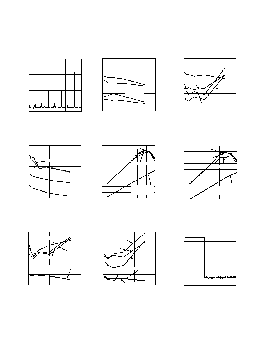
0
≠10
≠20
≠30
≠40
≠50
≠70
≠60
≠80
≠90
START: 0Hz
STOP: 40MHz
10dB ≠ Div
≠100
Figure 4. Single-Tone SFDR (DC to
2 f
DATA
, f
CLOCK
= 2 f
DATA
)
f
OUT
≠ MHz
dB
75
70
60
65
2.0
4.0
10.0
S/E 0dBFS
DIFF 0dBFS
S/E ≠6dBFS
DIFF ≠6dBFS
55
50
0
6.0
8.0
Figure 7. "Out-of-Band" SFDR vs. f
OUT
(f
DATA
/2 to 3/2 f
DATA
)
f
OUT
≠ MHz
dB
80
70
SFDR @ 10mA
65
2
75
60
55
0
SINAD @ 10mA
SFDR @ 5mA
SINAD @ 5mA
SFDR @ 2.5mA
SINAD @ 2.5mA
4
6
8
10
Figure 10. SINAD/SFDR vs. I
OUTFS
(DC to f
DATA
/2, Differential Output)
Typical AC Characterization Curves @ +5 V Supplies
(AVDD = +5 V, DVDD = +5 V, 50 Doubly Terminated Load, T
A
= +25 C, f
CLOCK
= 40 MSPS, unless otherwise noted, worst of I or Q output
performance shown)
f
OUT
≠ MHz
dB
65
60
50
55
0
2.0
10.0
4.0
6.0
8.0
10.5
9.67
8.01
8.84
ENOB
S/E 0dBFS
DIFF 0dBFS
S/E ≠6dBFS
DIFF ≠6dBFS
Figure 5. SINAD (ENOBs) vs. f
OUT
(DC
to f
DATA
/2)
A
OUT
≠ dBFS
dB
80
75
60
65
≠25
≠20
≠5
SFDR @ 40MSPS
55
50
≠30
≠15
≠10
SINAD @ 40MSPS
SFDR @ 20MSPS
SINAD @ 20MSPS
SFDR @ 10MSPS
SINAD @ 10MSPS
70
45
40
35
≠0
Figure 8. SINAD vs. A
OUT
(DC to
f
DATA
/2, Differential Output)
f
OUT
≠ MHz
dB
80
70
SFDR @ 10mA
65
2
75
60
55
0
SINAD @ 10mA
SFDR @ 5mA
SINAD @ 5mA
SFDR @ 2.5mA
SINAD @ 2.5mA
4
6
8
10
Figure 11. SINAD/SFDR vs. I
OUTFS
(DC to f
DATA
/2, Single-Ended Output)
f
OUT
≠ MHz
dB
80
75
65
70
0
5.0
10.0
S/E 0dBFS
DIFF 0dBFS
S/E ≠6dBFS
DIFF ≠6dBFS
Figure 6. SFDR vs. f
OUT
(DC to f
DATA
/2)
A
OUT
≠ dBFS
dB
80
75
60
65
≠25
≠20
≠5
SFDR @ 40MSPS
55
50
≠30
≠15
≠10
SINAD @ 40MSPS
SFDR @ 20MSPS
SINAD @ 20MSPS
SFDR @ 10MSPS
SINAD @ 10MSPS
70
45
40
35
0
Figure 9. SINAD vs. A
OUT
(DC to
f
DATA
/2, Single-Ended Output)
≠45
≠65
≠55
≠75
≠85
START: 0Hz
STOP: 20MHz
10dB ≠ Div
≠105
≠95
Figure 12. Wideband Spread-
Spectrum Spectral Plot (DC to f
DATA
)
AD9761
≠9≠
REV. A
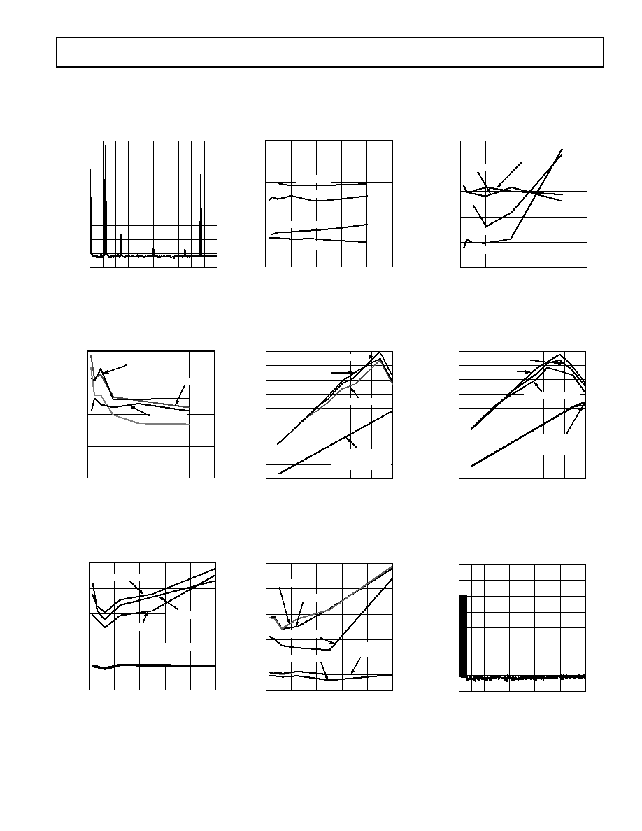
Typical AC Characterization Curves @ +3 V Supplies
(AVDD = +3 V, DVDD = +3 V, 50 Doubly Terminated Load, T
A
= +25 C, f
CLOCK
= 10 MSPS, unless otherwise noted, worst of I or Q output
performance shown)
0
≠10
≠20
≠30
≠40
≠50
≠70
≠60
≠80
≠90
START: 0Hz
STOP: 10MHz
10dB ≠ Div
Figure 13. Single-Tone SFDR (DC to
2 f
DATA
, f
CLOCK
= 2 f
DATA
)
f
OUT
≠ MHz
dB
75
70
60
65
0
0.5
2.5
1.0
1.5
2.0
S/E 0dBFS
DIFF 0dBFS
S/E ≠6dBFS
DIFF ≠6dBFS
80
Figure 16. "Out-of-Band" SFDR vs.
f
OUT
(f
DATA
/2 to 3/2f
DATA
)
f
OUT
≠ MHz
dB
80
70
SFDR @ 10mA
65
2
75
60
55
0
SINAD @ 10mA
SFDR @ 5mA
SINAD @ 5mA
SFDR @ 2.5mA
SINAD @ 2.5mA
4
6
8
10
Figure 19. SINAD/SFDR vs. I
OUTFS
(DC
to f
DATA
/2, Differential Output)
f
OUT
≠ MHz
dB
65
60
50
55
0
0.5
2.5
1.0
1.5
2.0
10.5
9.67
8.01
8.84
ENOB
S/E 0dBFS
DIFF 0dBFS
S/E ≠6dBFS
DIFF ≠6dBFS
Figure 14. SINAD (ENOBs) vs. f
OUT
(DC to f
DATA
/2)
A
OUT
≠ dBFS
dB
75
70
60
65
≠30
≠25
≠5
≠20
≠15
≠10
SFDR @ 40MSPS
80
SFDR @ 20MSPS
SFDR @ 10MSPS
SINAD @ 40MSPS
SINAD @ 20MSPS
SINAD @ 10MSPS
55
50
45
40
35
0
Figure 17. SINAD vs. A
OUT
(DC to
f
DATA
/2, Differential Output)
SFDR @ 10mA
f
OUT
≠ MHz
dB
80
70
65
2
75
60
55
0
SINAD @ 10mA
SFDR @ 5mA
SINAD @ 5mA
SFDR @ 2.5mA
SINAD @ 2.5mA
4
6
8
10
Figure 20. SINAD/SFDR vs. I
OUTFS
(DC to f
DATA
/2, Single-Ended Output)
f
OUT
≠ MHz
dB
75
70
60
65
0
0.5
2.5
1.0
1.5
2.0
S/E 0dBFS
DIFF 0dBFS
S/E ≠6dBFS
DIFF ≠6dBFS
80
85
Figure 15. SFDR vs. f
OUT
(DC to f
DATA
/2)
A
OUT
≠ dBFS
dB
70
65
55
60
≠30
≠25
≠5
≠20
≠15
≠10
SFDR @ 40MSPS
75
SFDR @ 20MSPS
SFDR @ 10MSPS
SINAD @ 20MSPS
SINAD @ 10MSPS
50
45
40
35
30
0
SINAD @ 40MSPS
Figure 18. SINAD vs. A
OUT
(DC to
f
DATA
/2, Single-Ended Output)
0
≠10
≠20
≠30
≠40
≠50
≠70
≠60
≠80
START: 0Hz
STOP: 10MHz
10dB ≠ Div
Figure 21. Narrowband Spread-
Spectrum Spectral Plot (DC to f
DATA
)

AD9761
≠10≠
REV. A
FUNCTIONAL DESCRIPTION
Figure 22 shows a simplified block diagram of the AD9761. The
AD9761 is a complete dual channel, high speed, 10-bit CMOS
DAC capable of operating up to a 40 MHz clock rate. It has
been optimized for the transmit section of wideband communi-
cation systems employing I and Q modulation schemes. Excel-
lent matching characteristics between channels reduces the need
for any external calibration circuitry. Dual matching 2
◊
interpo-
lation filters included in the I and Q data path simplify any post,
bandlimiting filter requirements. The AD9761 interfaces with a
single 10-bit digital input bus that supports interleaved I and Q
input data.
ACOM
REFLO
"I"
DAC
FSADJ
IOUTA
IOUTB
WRITE INPUT
SELECT INPUT
DCOM
DVDD
CLOCK
AD9761
2
LATCH
"I"
REFIO
REFERENCE
COMP1
COMP2
COMP3
BIAS
GENERATOR
QOUTA
QOUTB
2
LATCH
"Q"
MUX
CONTROL
AVDD
DAC DATA
INPUTS
(10 BITS)
SLEEP
"Q"
DAC
Figure 22. Dual DAC Functional Block Diagram
Referring to Figure 22, the AD9761 consists of an analog sec-
tion and a digital section. The analog section includes matched
I and Q 10-bit DACs, a 1.20 V bandgap voltage reference and a
reference control amplifier. The digital section includes: two 2
◊
interpolation filters; segment decoding logic; and some addi-
tional digital input interface circuitry. The analog and digital
sections of the AD9761 have separate power supply inputs (i.e.,
AVDD and DVDD) that can operate over a 2.7 V to 5.5 V
range.
Each DAC consists of a large PMOS current source array ca-
pable of providing up to 10 mA of full-scale current, I
OUTFS
.
Each array is divided into 15 equal currents that make up the
four most significant bits (MSBs). The next four bits or middle
bits consist of 15 equal current sources whose value are 1/16th
of an MSB current source. The remaining LSBs are binary
weighted fractions of the middle-bits current sources. All of
these current sources are switched to one or the other of two
output nodes (i.e., IOUTA or IOUTB) via PMOS differential
current switches.
The full-scale output current, I
OUTFS
, of each DAC is regulated
from the same voltage reference and control amplifier, thus
ensuring excellent gain matching and drift characteristics be-
tween DACs. I
OUTFS
can be set from 1 mA to 10 mA via an
external resistor, R
SET
. The external resistor in combination
with both the reference control amplifier and voltage reference,
V
REFIO
, sets the reference current, I
REF
, which is mirrored over
to the segmented current sources with the proper scaling factor.
I
OUTFS
is exactly sixteen times the value of I
REF
.
The I and Q DACs are simultaneously updated on the rising
edge of CLOCK with digital data from their respective 2
◊
digi-
tal interpolation filters. The 2
◊
interpolation filters essentially
multiplies the input data rate of each DAC by a factor of two,
relative to its original input data rate while simultaneously re-
ducing the magnitude of first image associated with the DAC's
original input data rate. Since the AD9761 supports a single
10-bit digital bus with interleaved I and Q input data, the origi-
nal I and Q input data rate before interpolation is one-half the
CLOCK rate. After interpolation, the data rate into each I and
Q DAC becomes equal to the CLOCK rate.
The benefits of an interpolation filter are clearly seen in Figure
23, which shows an example of the frequency and time domain
representation of a discrete time sine wave signal before and
after it is applied to a digital interpolation filter. Images of the
sine wave signal appear around multiples of the DAC's input
data rate as predicted by the sampling theory. These undesirable
images will also appear at the output of a reconstruction DAC,
although modified by the DAC's sin(x)/(x) response. In many
bandlimited applications, these images must be suppressed by
an analog filter following the DAC. The complexity of this ana-
log filter is typically determined by the proximity of the desired
fundamental to the first image and the required amount of im-
age suppression.
FUNDAMENTAL
1
f
CLOCK
FUNDAMENTAL DIGITAL
FILTER
SUPPRESSED
"OLD"
1
ST
IMAGE
"NEW"
1ST IMAGE
f
CLOCK
1
ST
IMAGE
2
f
CLOCK
f
CLOCK
f
CLOCK
2
f
CLOCK
DACs
"SINX"
X
TIME DOMAIN
FREQUENCY DOMAIN
2x INTERPOLATION FILTER
INPUT DATA LATCH
DAC
f
CLOCK
f
CLOCK
2
f
CLOCK
2
f
CLOCK
2
2x
Figure 23. Time and Frequency Domain Example of Digital Interpolation Filter

AD9761
≠11≠
REV. A
Referring to Figure 23, the "new" first image associated with the
DAC's higher data rate after interpolation is "pushed" out fur-
ther relative to the input signal. The "old" first image associated
with the lower DAC data rate before interpolation is suppressed
by the digital filter. As a result, the transition band for the ana-
log reconstruction filter is increased thus reducing the complex-
ity of the analog filter.
The digital interpolation filters for I and Q paths are identical
43 tap halfband symmetric FIR filters. Each filter receives de-
interleaved I or Q data from the digital input interface. The
input CLOCK signal is internally divided by two to generate the
filter clock. The filters are implemented with two parallel paths
running at the filter clock rate. The output from each path is
selected on opposite phases of the filter clock, thus producing
interpolated filtered output data at the input clock rate. The
frequency response and impulse response of these filters are
shown in Figures 2a and 2b. Table I lists the idealized filter
coefficients that correspond to the filter's impulse response.
The digital section of the AD9761 also includes an input inter-
face section designed to support interleaved I and Q input data
from a single 10-bit bus. This section de-interleaves the I and Q
input data while ensuring its proper pairing for the 2
◊
interpola-
tion filters. A SLEEP/RESET input serves a dual function by
providing a reset function for this section as well as providing
power down functionality. Refer to the DIGITAL INPUT AND
INTERFACE CONSIDERATIONS and SLEEP/RESET
sections for a more detailed discussion.
DAC TRANSFER FUNCTION
Each I and Q DAC provides complementary current output
pins: IOUT(A/B) and QOUT(A/B) respectively. Note, QOUTA
and QOUTB operate identically to IOUTA and IOUTB.
IOUTA will provide a near full-scale current output, I
OUTFS
,
when all bits are high (i.e., DAC CODE = 1023) while IOUTB,
the complementary output, provides no current. The current
output of IOUTA and IOUTB are a function of both the input
code and I
OUTFS
and can be expressed as:
I
IOUTA
= (DAC CODE/1024)
◊
I
OUTFS
(1)
I
IOUTB
= (1023 ≠ DAC CODE)/1024
◊
I
OUTFS
(2)
where:
DAC CODE = 0 to 1023 (i.e., Decimal Representation).
As previously mentioned, I
OUTFS
is a function of the reference
current, I
REF
, which is nominally set by a reference, V
REFIO
, and
external resistor, R
SET
. It can be expressed as:
I
OUTFS
= 16
◊
I
REF
(3)
where:
I
REF
= V
REFIO
/R
SET
(4)
The two current outputs will typically drive a resistive load
directly or via a transformer. If dc coupling is required, IOUTA
and IOUTB should be directly connected to matching resistive
loads, R
LOAD
, which are tied to analog common, ACOM. Note,
R
LOAD
represents the equivalent load resistance seen by IOUTA
or IOUTB. The single-ended voltage output appearing at IOUTA
and IOUTB pins is simply:
V
IOUTA
= I
IOUTA
◊
R
LOAD
(5)
V
IOUTB
= I
IOUTB
◊
R
LOAD
(6)
Note, the full-scale value of V
IOUTA
and V
IOUTB
should not
exceed the specified output compliance range to maintain speci-
fied distortion and linearity performance.
The differential voltage, V
IDIFF
, appearing across IOUTA and
IOUTB is:
V
IDIFF
=(I
IOUTA
≠ I
IOUTB
)
◊
R
LOAD
(7)
Substituting the values of I
IOUTA
, I
IOUTB
, and I
REF
; V
IDIFF
can be
expressed as:
V
IDIFF
={(2 DAC CODE ≠ 1023)/1024)}
◊
(16 R
LOAD
/R
SET
)
◊
V
REFIO
(8)
These last two equations highlight some of the advantages of
operating the AD9761 differentially. First, differential operation
will help cancel common-mode error sources associated with
I
IOUTA
and I
IOUTB
such as noise and distortion. Second, the
differential code dependent current and subsequent voltage,
V
IDIFF
, is twice the value of the single-ended voltage output (i.e.,
V
IOUTA
or V
IOUTB
) thus providing twice the signal power to the
load.
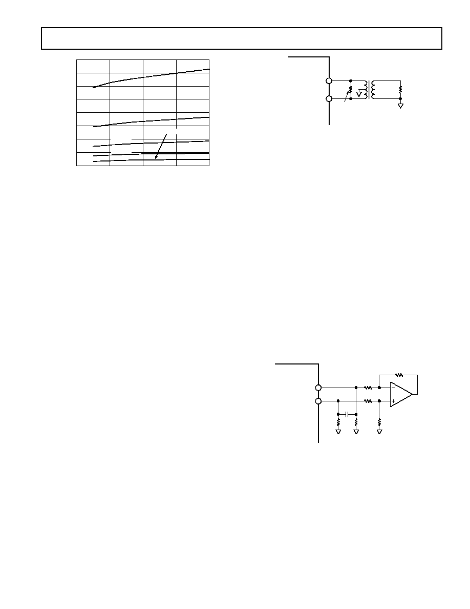
REFERENCE OPERATION
The AD9761 contains an internal 1.20 V bandgap reference
which can be easily disabled and overridden by an external
reference. REFIO serves as either an input or output depending
on whether the internal or an external reference is selected. If
REFLO is tied to ACOM as shown in Figure 24, the internal
reference is activated and REFIO provides a 1.20 V output. In
this case, the internal reference must be filtered externally with a
ceramic chip capacitor of 0.1
µ
F or greater from REFIO to
REFLO. Also, REFIO should be buffered with an external
amplifier having a low input bias current (i.e., <1
µ
A) if any
additional loading is required.
50pF
CURRENT
SOURCE
ARRAY
+1.2V REF
REFIO
FSADJ
REFLO
COMP2
AVDD
0.1 F
R
SET
2k
0.1 F
OPTIONAL EXTERNAL
REF BUFFER FOR
ADDITIONAL LOADS
COMPENSATION
CAPACITOR
REQUIRED
AD9761
Figure 24. Internal Reference Configuration
The internal reference can also be disabled by connecting REFLO
to AVDD. In this case, an external reference may then be ap-
plied to REFIO as shown in Figure 25. The external reference
may provide either a fixed reference voltage to enhance accuracy
and drift performance or a varying reference voltage for gain
control. Note that the 0.1
µ
F compensation capacitor is not
required since the internal reference is disabled and the high
input impedance (i.e., 1 M
) of REFIO minimizes any loading
of the external reference.

AD9761
≠12≠
REV. A
50pF
CURRENT
SOURCE
ARRAY
+1.2V REF
REFIO
FSADJ
REFLO
COMP2
AVDD
I
REF
=
V
REF
/R
SET
AVDD
R
SET
EXT.
V
REF
AVDD
0.1 F
AD9761
+
≠
Figure 25. External Reference Configuration
REFERENCE CONTROL AMPLIFIER
The AD9761 also contains an internal control amplifier which is
used to simultaneously regulate both DAC's full-scale output
current, I
OUTFS
. Since the I and Q I
OUTFS
are derived from the
same voltage reference and control circuitry, excellent gain
matching is ensured. The control amplifier is configured as a
V-I converter as shown in Figure 25 such that its current out-
put, I
REF
, is determined by the ratio of the V
REFIO
and an exter-
nal resistor, R
SET
, as stated in Equation (4). I
REF
is copied over
to the segmented current sources with the proper scaling factor
to set I
OUTFS
as stated in Equation (3).
The control amplifier allows a wide (10:1) adjustment span of
I
OUTFS
over a 1 mA to 10 mA range by setting I
REF
between
62.5
µ
A and 625
µ
A. The wide adjustment span of I
OUTFS
pro-
vides several application benefits. The first benefit relates di-
rectly to the power dissipation of the AD9761's analog supply,
AVDD, which is proportional to I
OUTFS
(refer to the POWER
DISSIPATION section). The second benefit relates to the
20 dB adjustment span which may be useful for system gain
control purposes.
Optimum noise and dynamic performance for the AD9761 is
obtained with a 0.1
µ
F external capacitor installed between
COMP2 and AVDD. The bandwidth of the reference control
amplifier is limited to approximately 5 kHz with a 0.1
µ
F ca-
pacitor installed. Since the ≠3 dB bandwidth corresponds to the
dominant pole and hence its dominant time constant, the set-
tling time of the control amplifier to a stepped reference input
response can be easily determined. Note, the output of the
control amplifier, COMP2, is internally compensated via a
50 pF capacitor thus ensuring its stability if no external capaci-
tor is added.
Depending on the requirements of the application, I
REF
can be
adjusted by varying either R
SET
, or in the external reference
mode, by varying the REFIO voltage. I
REF
can be varied for a
fixed R
SET
by disabling the internal reference and varying the
voltage of REFIO over its compliance range of 1.25 V to 0.10 V.
REFIO can be driven by a single-supply amplifier or DAC thus
allowing I
REF
to be varied for a fixed R
SET
. Since the input im-
pedance of REFIO is approximately 1 M
, a simple, low cost
R-2R ladder DAC configured in the voltage mode topology may
be used to control the gain. This circuit is shown in Figure 26
using the AD7524 and an external 1.2 V reference, the AD1580.
ANALOG OUTPUTS
As previously stated, both the I and Q DACs produce two
complementary current outputs which may be configured for
single-end or differential operation. I
IOUTA
and I
IOUTB
can be
converted into complementary single-ended voltage outputs,
V
IOUTA
and V
IOUTB
, via a load resistor, R
LOAD
, as described in
the DAC TRANSFER SECTION by Equations 5 through 8.
The differential voltage, V
IDIFF
, existing between V
IOUTA
and
V
IOUTB
can also be converted to a single-ended voltage via a
transformer or differential amplifier configuration.
Figure 27 shows an equivalent circuit of the AD9761's I (or Q)
DAC output. It consists of a parallel array of PMOS current
sources in which each current source is switched to either
IOUTA or IOUTB via a differential PMOS switch. As a result,
the equivalent output impedance of IOUTA and IOUTB re-
mains quite high (i.e., >100 k
and 5 pF).
AD9761
AVDD
R
LOAD
R
LOAD
IOUTA
IOUTB
Figure 27. Equivalent Circuit of the AD9761 DAC Output
IOUTA and IOUTB have a negative and positive voltage com-
pliance range which must be adhered to achieve optimum per-
formance. The negative output compliance range of ≠1 V is set
by the breakdown limits of the CMOS process. Operation be-
yond this maximum limit may result in a breakdown of the
output stage.
50pF
CURRENT
SOURCE
ARRAY
+1.2V REF
REFIO
FSADJ
REFLO
COMP2
AVDD
AVDD
AD1580
1.2V
OPTIONAL
BANDLIMITING
CAPACITOR
I
REF
=
V
REF
/R
SET
AVDD
R
SET
0.1V TO 1.2V
R
FB
V
DD
OUT1
OUT2
AGND
V
REF
AD7524
DB7≠DB0
+
≠
AD9761
Figure 26. Single-Supply Gain Control Circuit

AD9761
≠13≠
REV. A
The positive output compliance range is slightly dependent on
the full-scale output current, I
OUTFS
. It degrades slightly from
its nominal 1.25 V for an I
OUTFS
= 10 mA to 1.00 V for an
I
OUTFS
= 2 mA. Applications requiring the AD9761's output
(i.e., V
OUTA
and/or V
OUTB
) to extend to its output compliance
range should size R
LOAD
accordingly. Operation beyond this
compliance range will adversely affect the AD9761's linearity
performance and subsequently degrade its distortion perfor-
mance. Note, the optimum distortion performance of the
AD9761 is obtained by restricting its output(s) as seen at
IOUT(A/B) and QOUT(A/B) to within
±
0.5 V.
DIGITAL INPUTS AND INTERLEAVED INTERFACE
CONSIDERATIONS
The AD9761 digital interface consists of 10 data input pins, a
clock input pin, and three control pins. It is designed to support
a clock rate up to 40 MSPS. The 10-bit parallel data inputs
follow standard positive binary coding, where DB9 is the most
significant bit (MSB) and DB0 is the least significant bit (LSB).
IOUTA (or QOUTA) produces a full-scale output current when
all data bits are at Logic 1. IOUTB (or QOUTB) produces a
complementary output, with the full-scale current split between
the two outputs as a function of the input code.
STATE
MACHINE
"I" AND "Q" DATA
CLOCK
SELECT
RESET/SLEEP
WRITE
"Q" DATA
CLOCK
2
"I" DATA
"I"
INPUT
REGISTER
"I"
FILTER
REGISTER
"Q"
INPUT
REGISTER
"Q"
INPUT
REGISTER
Figure 28. Block Diagram of Digital Interface
The AD9761 interfaces with a single 10-bit digital input bus
that supports interleaved I and Q input data. Figure 28 shows a
simplified block diagram of the digital interface circuitry consist-
ing of two banks of edge triggered registers, two multiplexers,
and a state machine. Interleaved I and Q input data is presented
at the DATA input bus, where it is then latched into the se-
lected I or Q input register on the rising edge of the WRITE
input. The output of these input registers is transferred in pairs
to their respective interpolator filters' register after each Q write
on the rising edge of the CLOCK input (refer to Timing Dia-
gram in Figure 2). A state machine ensures the proper pairing of
I and Q input data to the interpolation filter's inputs.
The SELECT signal at the time of the rising edge of the WRITE
signal determines which input register latches the input data. If
SELECT is high around the rising edge of WRITE the data is
latched into the I register of the AD9761. If SELECT is low
around the rising edge of the WRITE, the data is latched into
the Q register of the AD9761. If SELECT is kept in one state
while data is repeatedly writing to the AD9761, the data will be
written into the selected filter register at half the input data rate
since the data is always assumed to be interleaved.
The state machine controls the generation of the divided clock
and hence pairing of I and Q data inputs. After the AD9761 is
reset, the state machine keeps track of the paired I and Q data.
The state transition diagram is shown in Figure 29, in which all
the states are defined. A transition in state occurs upon the
rising edge of CLOCK and is a function of the current state as
well as status of SELECT, WRITE and SLEEP. The state ma-
chine is reset on the first rising CLOCK edge while RESET
remains high. Upon RESET returning low, a state transition will
occur on the first rising edge of CLOCK. The most recent I and Q
data samples are transferred to the correct interpolation filter
only upon entering state FILTER DATA.
Note, it is possible to ensure proper pairing of I and Q
data inputs without issuing RESET high. This may be
accomplished by writing two or more successive Q data
inputs followed by a clock. In this case, the state machine
will advance to either the RESET or FILTER DATA state.
The state machine will advance to the ONE-I state upon
writing I data followed by a clock.
ONE, I
RESET
FILTER
DATA
I or Q or N
N
I = WRITE & SELECT FOLLOWED BY A CLOCK
Q = WRITE &
SELECT
FOLLOWED BY A CLOCK
N = CLOCK ONLY, NO WRITE
I
I
Q
Q or N
Figure 29. State Transition Diagram of AD9761 Digital
Interface
An example helps illustrate the digital timing and control re-
quirements to ensure proper pairing of I and Q data. In this
example, the AD9761 is assumed to interface with a host pro-
cessor on a dedicated data bus and the state machine is reset by
asserting a Logic Level "1" to the RESET/SLEEP input for a
duration of one clock cycle. In the timing diagram shown in
Figure 30, WRITE and CLOCK are tied together while SELECT
is updated at the same instance as DATA. Since SELECT is
high upon RESET returning low, I data is latched into the I
input register on the first rising WRITE. On the next rising
WRITE edge, the Q data is latched into its input register and
the outputs of both input registers are latched into their respec-
tive I and Q filter registers. The sequence of events is repeated
on the next rising WRITE edge with the new I data being
latched into the I input register.
The digital inputs are CMOS compatible with logic thresholds,
V
THRESHOLD
set to approximately half the digital positive supply
(DVDD) or V
THRESHOLD
= DVDD/2 (
±
20%).
The internal digital circuitry of the AD9761 is capable of oper-
ating over a digital supply range of 2.7 V to 5.5 V. As a result,
the digital inputs can also accommodate TTL levels when DVDD
is set to accommodate the maximum high level voltage, V
OH(MAX)
,
of the TTL drivers. A DVDD of 3 V to 3.3 V will typically

AD9761
≠14≠
REV. A
ensure proper compatibility of most TTL logic families. Figure
31 shows the equivalent digital input circuit for the data, sleep
and clock inputs.
RESET
DATA
SELECT
CLOCK/WRITE
I
0
Q
0
I
1
Q
1
Figure 30. Timing Diagram
DVDD
DIGITAL
INPUT
Figure 31. Equivalent Digital Input
Since the AD9761 is capable of being updated up to 40 MSPS,
the quality of the clock and data input signals are important in
achieving the optimum performance. The drivers of the digital
data interface circuitry should be specified to meet the mini-
mum setup and hold-times of the AD9761 as well as its re-
quired min/max input logic level thresholds. The external clock
driver circuitry should provide the AD9761 with a low jitter
clock input meeting the min/max logic levels while providing
fast edges. Fast clock edges will help minimize any jitter that can
manifest itself as phase noise on a reconstructed waveform.
Digital signal paths should be kept short, and run lengths
matched to avoid propagation delay mismatch. The insertion of
a low value resistor network (i.e., 20
to 100
) between the
AD9761 digital inputs and driver outputs may be helpful in
reducing any overshooting and ringing at the digital inputs,
which contributes to data feedthrough. Operating the AD9761
with reduced logic swings and a corresponding digital supply
(DVDD) will also reduce data feedthrough.
RESET/SLEEP MODE OPERATION
The RESET/SLEEP input can be used either to power-down
the AD9761 or reset its internal digital interface logic. If the
RESET/ SLEEP input is asserted for greater than one clock
cycle but under four clock cycles by applying a logic level "1,"
the internal state machine will be reset. If the RESET/SLEEP
input is asserted for four clock cycles or longer, the power-down
function of the AD9761 will be initiated. The power-down
function turns off the output current and reduces the supply
current to less than 9 mA over the specified supply range of
2.7 V to 5.5 V and temperature range.
The power-up and power-down characteristics of the AD9761 is
dependent upon the value of the compensation capacitor con-
nected to COMP1 and COMP3. With a nominal value of 0.1
µ
F,
the AD9761 takes less than 5
µ
s to power down and approxi-
mately 3.25 ms to power back up.
POWER DISSIPATION
The power dissipation of the AD9761 is dependent on several
factors which include: (1) AVDD and DVDD, the power supply
voltages; (2) I
OUTFS
, the full-scale current output; (3) f
CLOCK
, the
update rate; (4) and the reconstructed digital input waveform.
The power dissipation is directly proportional to the analog
supply current, I
AVDD
, and the digital supply current, I
DVDD
.
I
AVDD
is directly proportional to I
OUTFS
as shown in Figure 32
and is insensitive to f
CLOCK
.
I
OUTFS
≠ mA
30
0
1
10
2
3
4
5
6
7
8
9
25
20
15
10
5
I
AVDD
≠ mA
Figure 32. I
AVDD
vs. I
OUTFS
Conversely, I
DVDD
is dependent on both the digital input wave-
form, f
CLOCK
, and digital supply DVDD. Figures 33 and 34 show
I
DVDD
as a function of a full-scale sine wave output ratio's (f
OUT
/
f
CLOCK
) for various update rate with DVDD = 5 V and DVDD =
3 V respectively.
5 MSPS
RATIO ≠ f
OUT
/f
CLK
40
30
0.05
0.15
40 MSPS
20
0
0.1
20 MSPS
10 MSPS
10
0
I
DVDD
≠ mA
0.2
50
60
70
2.5 MSPS
Figure 33. I
DVDD
vs. Ratio @ DVDD = 5 V
AD9761
≠15≠
REV. A
5 MSPS
RATIO ≠ f
OUT
/f
CLK
40
30
0.05
0.15
40 MSPS
20
0
0.1
20 MSPS
10 MSPS
10
0
I
DVDD
≠ mA
0.2
2.5 MSPS
5
35
25
15
Figure 34. I
DVDD
vs. Ratio @ DVDD = 3 V
APPLYING THE AD9761
OUTPUT CONFIGURATIONS
The following sections illustrate some typical output configura-
tions for the AD9761. Unless otherwise noted, it is assumed
that I
OUTFS
is set to a nominal 10 mA. For applications requir-
ing the optimum dynamic performance, a differential output
configuration is suggested. A differential output configuration
may consist of either an RF transformer or a differential op amp
configuration. The transformer configuration provides the opti-
mum high frequency performance and is recommended for any
application allowing for ac coupling. The differential op amp
configuration is suitable for applications requiring dc coupling, a
bipolar output, signal gain, and/or level shifting.
A single-ended output is suitable for applications requiring a
unipolar voltage output. A positive unipolar output voltage will
result if IOUTA and/or IOUTB is connected to an appropri-
ately sized load resistor, R
LOAD
, referred to ACOM. This
configuration may be more suitable for a single-supply system
requiring a dc coupled, ground referred output voltage. Alterna-
tively, an amplifier could be configured as an I-V converter thus
converting I
OUTA
or I
OUTB
into a negative unipolar voltage. This
configuration provides the best dc linearity since IOUTA or
IOUTB is maintained at a virtual ground.
DIFFERENTIAL COUPLING USING A TRANSFORMER
An RF transformer can be used to perform a differential-to-
single-ended signal conversion as shown in Figure 35. A differen-
tially coupled transformer output provides the optimum distortion
performance for output signals whose spectral content lies within
the transformers passband. An RF transformer such as the Mini
Circuits T1-1T provides excellent rejection of common-mode
distortion (i.e., even-order harmonics) and noise over a wide
frequency range. It also provides electrical isolation and the
ability to deliver twice the power to the load. Transformers with
different impedance ratios may also be used for impedance
matching purposes. Note that the transformer provides ac cou-
pling only.
OPTIONAL
R
DIFF
R
LOAD
MINI-CIRCUITS
T1-1T
IOUTA
IOUTB
AD9761
Figure 35. Differential Output Using a Transformer
The center-tap on the primary side of the transformer must be
connected to ACOM to provide the necessary dc current path
for both I
OUTA
and I
OUTB
. The complementary voltages appear-
ing at IOUTA and IOUTB (i.e., V
OUTA
and V
OUTB
) swing sym-
metrically around ACOM and should be maintained with the
specified output compliance range of the AD9761. A differential
resistor, R
DIFF
, may be inserted in applications in which the
output of the transformer is connected to the load, R
LOAD
, via a
passive reconstruction filter or cable requiring double termina-
tion. R
DIFF
is determined by the transformer's impedance ratio
and provides the proper source termination which results in a
low VSWR. Note that approximately half the signal power will
be dissipated across R
DIFF
.
DIFFERENTIAL USING AN OP AMP
An op amp can also be used to perform a differential to single-
ended conversion as shown in Figure 36. The AD9761 is config-
ured with two equal load resistors, R
LOAD
, of 50
. The differential
voltage developed across IOUTA and IOUTB is converted to a
single-ended signal via the differential op amp configuration. An
optional capacitor can be installed across IOUTA and IOUTB
forming a real pole in a low-pass filter. The addition of this
capacitor also enhances the op amps distortion performance by
preventing the DACs high slewing output from overloading the
op amp's input.
C
OPT
200
500
IOUTA
IOUTB
AD9761
R
LOAD
50
200
AD8042
500
R
LOAD
50
Figure 36. DC Differential Coupling Using an Op Amp
The common-mode rejection of this configuration is typically
determined by the resistor matching. In this circuit, the differen-
tial op amp circuit using the AD8042 is configured to provide
some additional signal gain. The op amp must operate from a
dual supply since its output is approximately
±
1.0 V. A high
speed amplifier capable of preserving the differential performance
of the AD9761 while meeting other system level objectives (i.e.,
cost, power) should be selected. The op amps differential gain, its
gain setting resistor values, and full-scale output swing capabili-
ties should all be considered when optimizing this circuit.

AD9761
≠16≠
REV. A
The differential circuit shown in Figure 37 provides the neces-
sary level-shifting required in a single supply system. In this
case, AVDD, which is the positive analog supply for both the
AD9761 and the op amp is also used to level-shift the differen-
tial output of the AD9761 to midsupply (i.e., AVDD/2).
C
OPT
200
1k
IOUTA
IOUTB
AD9761
R
LOAD
50
200
AD8042
500
R
LOAD
50
1k
AVDD
Figure 37. Single-Supply DC Differential Coupled
Circuit
SINGLE-ENDED UNBUFFERED VOLTAGE OUTPUT
Figure 38 shows the AD9761 configured to provide a unipolar
output range of approximately 0 V to +0.5 V since the nominal
full-scale current, I
OUTFS
, of 10 mA flows through an R
LOAD
of
50
. In the case of a doubly terminated low-pass filter, R
LOAD
represents the equivalent load resistance seen by IOUTA or
IOUTB. The unused output (IOUTA or IOUTB) can be con-
nected to ACOM directly or via a matching R
LOAD
. Different
values of I
OUTFS
and R
LOAD
can be selected as long as the posi-
tive compliance range is adhered to.
50
IOUTA
IOUTB
AD9761
50
I
OUTFS
= 10mA
V
OUT
=
0V TO 0.5V
Figure 38. 0 V to +0.5 V Unbuffered Voltage Output
DIFFERENTIAL, DC COUPLED OUTPUT
CONFIGURATION WITH LEVEL SHIFTING
Some applications may require the AD9761 differential outputs
to interface to a single supply quadrature upconverter. Although
most of these devices provide differential inputs, its common-
mode voltage range does not typically extend to ground. As a
result, the ground-referenced output signals shown in Figure 38
must be level shifted to within the specified common-mode
range of the single-supply quadrature upconverter. Figure 39
shows the addition of a resistor pull-up network which provides
the level shifting function. The use of matched resistor networks
will maintain maximum gain matching and minimum offset
performance between the I and Q channels. Note, the resistor
pull-up network will introduce approximately 6 dB of signal
attenuation.
50
**
IOUTA
IOUTB
AD9761
50
**
500
*
500
*
500
*
500
*
AVDD
V
IN+
V
IN≠
QUADRATURE
UPCONVERTER
*
OHMTEK TO MC-1603-5000D
**
OHMTEK TO MC-1603-1000D
Figure 39. Differential, DC Coupled Output Configuration
with Level-Shifting
POWER AND GROUNDING CONSIDERATIONS
In systems seeking to simultaneously achieve high speed and
high performance, the implementation and construction of the
printed circuit board design is often as important as the circuit
design. Proper RF techniques must be used in device selection;
placement and routing; and supply bypassing and grounding.
The evaluation board for the AD9761, which uses a four-layer
PC board, serves as a good example for the above mentioned
considerations. The evaluation board provides an illustration of
the recommended printed circuit board ground, power and
signal plane layout.
Proper grounding and decoupling should be a primary objective
in any high speed, high resolution system. The AD9761 features
separate analog and digital supply and ground pins to optimize
the management of analog and digital ground currents in a system.
In general, AVDD, the analog supply, should be decoupled to
ACOM, the analog common, as close to the chip as physically
possible. Similarly, DVDD, the digital supply should be decoupled
as closely as physically as possible to DCOM.
For those applications requiring a single +5 V or +3 V supply
for both the analog and digital supply, a clean analog supply
may be generated using the circuit shown in Figure 40. The
circuit consists of a differential LC filter with separate power
supply and return lines. Lower noise can be attained using low
ESR type electrolytic and tantalum capacitors.
0.1 F
CER.
10-22 F
TANT.
100 F
ELECT.
AVDD
ACOM
+
+
≠
≠
FERRITE
BEADS
+5V OR +3V POWER
SUPPLY
TTL/CMOS
LOGIC
CIRCUITS
Figure 40. Differential LC Filter for Single +5 V or +3 V
Applications
AD9761
≠17≠
REV. A
Maintaining low noise on power supplies and ground is critical
to obtaining optimum results from the AD9761. If properly
implemented, ground planes can perform a host of functions on
high speed circuit boards: bypassing, shielding, current trans-
port, etc. In mixed signal design, the analog and digital portions
of the board should be distinct from each other, with the analog
ground plane confined to the areas covering the analog signal
traces and the digital ground plane confined to areas covering
the digital interconnects.
All analog ground pins of the DAC, reference and other analog
components should be tied directly to the analog ground plane.
The two ground planes should be connected by a path 1/8 to 1/4
inch wide underneath, or within 1/2 inch of the DAC to main-
tain optimum performance. Care should be taken to ensure that
the ground plane is uninterrupted over crucial signal paths. On
the digital side, this includes the digital input lines running to
the DAC as well as any clock signals. On the analog side, this
includes the DAC output signal, reference signal and the supply
feeders.
The use of wide runs or planes in the routing of power lines is
also recommended. This serves the dual role of providing a low
series impedance power supply to the part, as well as providing
some "free" capacitive decoupling to the appropriate ground
plane. It is essential that care be taken in the layout of signal and
power ground interconnects to avoid inducing extraneous volt-
age drops in the signal ground paths. Its is recommended that
all connections be short, direct and as physically close to the
package as possible, in order to minimize the sharing of conduc-
tion paths between different currents. When runs exceed an inch
in length, strip line techniques with proper termination resistor
should be considered. The necessity and value of this resistor
will be dependent upon the logic family used.
For a more detailed discussion of the implementation and con-
struction of high speed, mixed signal printed circuit boards,
refer to Analog Devices' application notes AN-280 and AN-333.
APPLICATIONS
Using the AD9761 for QAM Modulation
QAM is one of the most widely used digital modulation schemes
in digital communication systems. This modulation technique
can be found in both FDM as well as spread spectrum (i.e.,
CDMA) based systems. A QAM signal is a carrier frequency
that is modulated both in amplitude (i.e., AM modulation) and
in phase (i.e., PM modulation). It can be generated by indepen-
dently modulating two carriers of identical frequency but with a
90
∞
phase difference. This results in an in-phase (I) carrier com-
ponent and a quadrature (Q) carrier component at a 90
∞
phase
shift with respect to the I component. The I and Q components
are then summed to provide a QAM signal at the specified car-
rier frequency.
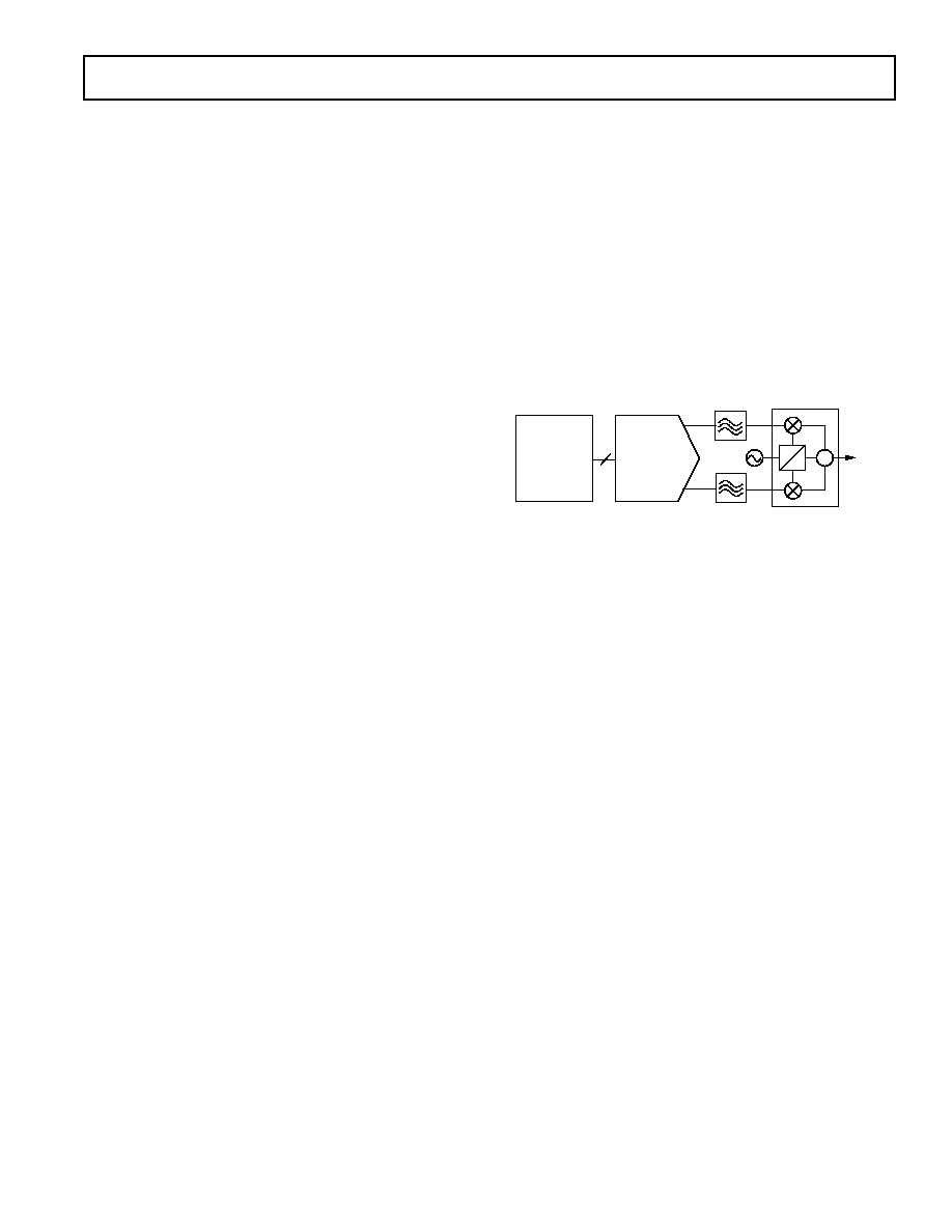
A common and traditional implementation of a QAM modula-
tor is shown in Figure 41. The modulation is performed in the
analog domain in which two DACs are used to generate the
baseband I and Q components, respectively. Each component is
then typically applied to a Nyquist filter before being applied to
a quadrature mixer. The matching Nyquist filters shapes and
limits each component's spectral envelope while minimizing
intersymbol interference. The DAC is typically updated at the
QAM symbol rate or possibly a multiple of it if an interpolating
filter precedes the DAC. The use of an interpolating filter typi-
cally eases the implementation and complexity of the analog
filter which can be a significant contributor to mismatches in
gain and phase between the two baseband channels. A quadra-
ture mixer modulates the I and Q components with in-phase
and quadrature phase carrier frequency and then sums the two
outputs to provide the QAM signal.
0
90
CARRIER
FREQ
NYQUIST
FILTERS
QUADRATURE
MODULATOR
TO
MIXER
IOUT
QOUT
AD9761
10
DSP
OR
ASIC
Figure 41. Typical Analog QAM Architecture
EVALUATION BOARD
The AD9761-EB is an evaluation board for the AD9761 dual
10-bit, 40 MSPS DAC. Careful attention to layout and circuit
design along with prototyping area, allows the user to easily and
effectively evaluate the AD9761. This board allows the user the
flexibility to operate each of the AD9761 DACs in a single-
ended or differential output configuration. Each of the DACs'
single-ended outputs are terminated in a 50
resistor. Evaluation
using a transformer coupled output can be accomplished simply
by installing a Minicircuit transformer (i.e., Model T2-1T) into
the available socket.
The digital inputs are designed to be driven directly from vari-
ous word generators with the onboard option to add a resistor
network for proper load termination. Separate 50
terminated
SMA connectors are also provided for the CLOCK, WRITE
and SELECT inputs. Provisions are also made to operate the
AD9761 with either the internal or an external reference as well
as to exercise the power-down feature.

AD9761
≠18≠
REV. A
Figure 42a. Evaluation Board Schematic

AD9761
≠19≠
REV. A
Figure 42b. Evaluation Board Schematic

AD9761
≠20≠
REV. A
Figure 43. Silkscreen Layer--Top
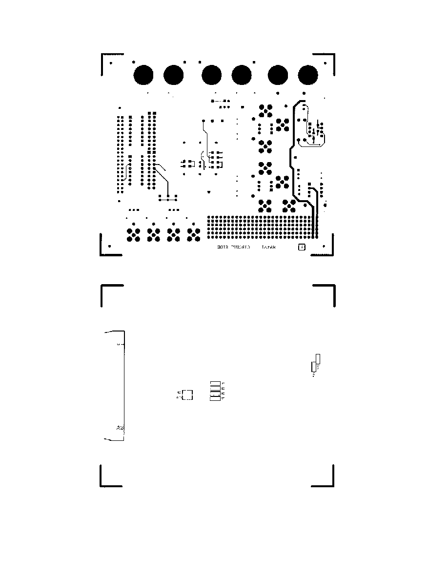
Figure 44. Component Side PCB Layout (Layer 1)

AD9761
≠21≠
REV. A
Figure 45. Ground Plane PCB Layout (Layer 2)
Figure 46. Power Plane PCB Layout (Layer 3)
AD9761
≠22≠
REV. A
Figure 47. Solder Side PCB Layout (Layer 4)
Figure 48. Silkscreen Layer--Bottom

AD9761
≠23≠
REV. A
28-Lead Shrink Small Outline Package (SSOP)
(RS-28)
28
15
14
1
0.407 (10.34)
0.397 (10.08)
0.311 (7.9)
0.301 (7.64)
0.212 (5.38)
0.205 (5.21)
PIN 1
SEATING
PLANE
0.008 (0.203)
0.002 (0.050)
0.07 (1.79)
0.066 (1.67)
0.0256
(0.65)
BSC
0.078 (1.98)
0.068 (1.73)
0.015 (0.38)
0.010 (0.25)
0.009 (0.229)
0.005 (0.127)
0.03 (0.762)
0.022 (0.558)
8
0
OUTLINE DIMENSIONS
Dimensions shown in inches and (mm).
PRINTED IN U.S.A.
C3150≠0≠2/00 (rev. A)