 | –≠–ª–µ–∫—Ç—Ä–æ–Ω–Ω—ã–π –∫–æ–º–ø–æ–Ω–µ–Ω—Ç: ADD8704 | –°–∫–∞—á–∞—Ç—å:  PDF PDF  ZIP ZIP |

16 V Quad
Operational Amplifier
ADD8704
FEATURES
Single-supply operation: 4.5 V to 16.5 V
Upper/lower buffers swing to V
DD
/GND
Continuous output current: 35 mA
V
COM
peak output current: 250 mA
Offset voltage: 15 mV
Slew rate: 6 V/µs
Unity gain stable with large capacitive loads
Supply current: 700 µA per amplifier
Drop-in replacement for EL5420
APPLICATIONS
TFT LCD monitor panels
TFT LCD notebook panels
Communications equipment
Portable instrumentation
Electronic games
GENERAL DESCRIPTION
The ADD8704 is a single-supply quad operational amplifier that
has been optimized for today's low cost TFT LCD notebook and
monitor panels. Output channels A and D swing to the rail for
use as end-point gamma references. Output channels B and C
provide high continuous and peak current drive for use as V
COM
or repair amplifiers; they can also be used as midpoint gamma
references. All four amplifiers have excellent transient response
and have high slew rate and capacitive load drive capability. The
ADD8704 is specified over the ≠40∞C to +85∞C temperature
range and is available in either a 14-lead TSSOP or a 16-lead
LFCSP package for thin, portable applications.
Table 1. Input/Output Characteristics
Channel V
IH
V
IL
I
O
(mA)
I
SC
(mA)
A V
DD
≠ 1.7 V
GND
15
150
B V
DD
≠ 1.7 V
GND
35
250
C V
DD
GND 35
250
D V
DD
GND + 1.7 V
15
150
Rev. 0
PIN CONFIGURATIONS
1
2
3
4
5
6
7
14
13
12
11
10
9
8
ADD8704
OUT B
≠IN B
+IN B
V+
V≠
+IN A
≠IN A
OUT A
OUT C
≠IN C
+IN C
+IN D
≠IN D
OUT D
00001-0-0-1
+
≠
+ ≠
+
≠
+ ≠
Figure 1. 14-Lead TSSOP (RU Suffix)
12
≠IN D
11
+IN D
10
V≠
9
+IN C
≠IN A
1
+IN A
2
V+
3
≠IN
A
5
OUT B
6
OUT C
7
≠I
N C
8
+IN B
4
16
NC
15
OUT A
14
OUT D
13
NC
ADD8704
TOP VIEW
00001-0-002
Figure 2. 16-Lead CSP (CP Suffix)
Information furnished by Analog Devices is believed to be accurate and reliable.
However, no responsibility is assumed by Analog Devices for its use, nor for any
infringements of patents or other rights of third parties that may result from its use.
Specifications subject to change without notice. No license is granted by implication
or otherwise under any patent or patent rights of Analog Devices. Trademarks and
registered trademarks are the property of their respective owners.
One Technology Way, P.O. Box 9106, Norwood, MA 02062-9106, U.S.A.
Tel: 781.329.4700
www.analog.com
Fax: 781.326.8703
© 2003 Analog Devices, Inc. All rights reserved.

ADD8704
TABLE OF CONTENTS
Electrical Characteristics ................................................................. 3
Absolute Maximum Ratings............................................................ 5
Typical Performance Characteristics ............................................. 6
Application Information................................................................ 12
Theory.......................................................................................... 12
Input............................................................................................. 12
Output.......................................................................................... 12
Important Note........................................................................... 12
Outline Dimensions ....................................................................... 14
Ordering Guide .......................................................................... 14
REVISION HISTORY
Revision 0: Initial Version
Rev. 0 | Page 2 of 16

ADD8704
ELECTRICAL CHARACTERISTICS
Table 2. V
S
= 16 V, V
CM
= V
S
/2, T
A
@ 25
∞
C, unless otherwise noted
Parameter
Symbol Condition
Min Typ
Max Unit
INPUT CHARACTERISTICS
Offset Voltage
V
OS
2 15
mV
Offset Voltage Drift
V
OS
/
T
≠40∞C T
A
+85∞C
10
µV/∞C
Input Bias Current
I
B
200
1100
nA
≠40∞C T
A
+85∞C
1500
nA
Input Offset Current
I
OS
10
100
nA
≠40∞C T
A
+85∞C
250
nA
Common-Mode Rejection Ratio
CMRR
≠40∞C T
A
+85∞C
Amp A
V
CM
= 0 to (V
S
≠ 1.7 V)
54
95
dB
Amp B
V
CM
= 0 to (V
S
≠ 1.7 V)
54
95
dB
Amp C
V
CM
= 0 to V
S
54
95
dB
Amp D
V
CM
= 1.7 V to V
S
54
95
dB
Large Signal Voltage Gain
AVO
R
L
= 10 k, V
O
= 0.5 to (V
S
≠ 0.5 V)
1
10
V/mV
Input Impedance
Z
IN
400
k
Input Capacitance
C
IN
1 pF
OUTPUT CHARACTERISTIS
Output Voltage High (A)
V
OH
I
L
= 100 µA
15.985
V
Optimized for Low Swing
I
L
= 5 mA
15.6
15.75
V
≠40∞C T
A
+85∞C
15.5
V
Output Voltage High (B)
V
OH
I
L
= 100 µA
15.995
V
Optimized for V
COM
I
L
= 5 mA
15.8
15.9
V
≠40∞C T
A
+85∞C
15.75
V
Output Voltage High (C)
V
OH
I
L
= 100 µA
15.995
V
Optimized for Midrange
I
L
= 5 mA
15.8
15.9
V
≠40∞C T
A
+85∞C
15.75
V
Output Voltage High (D)
V
OH
I
L
= 100 µA
15.99
V
Optimized for High Swing
I
L
= 5 mA
15.75
15.85
V
≠40∞C T
A
+85∞C
15.65
V
Output Voltage Low (A)
V
OL
I
L
= 100 µA
20
mV
Optimized for Low Swing
I
L
= 5 mA
80
200
mV
≠40∞C T
A
+85∞C
300
mV
Output Voltage Low (B)
V
OL
I
L
= 100 µA
5
mV
Optimized for V
COM
I
L
= 5 mA
50
150
mV
≠40∞C T
A
+85∞C
250
mV
Output Voltage Low (C)
V
OL
I
L
= 100 µA
5
mV
Optimized for Midrange
I
L
= 5 mA
50
150
mV
≠40∞C T
A
+85∞C
250
mV
Output Voltage Low (D)
V
OL
I
L
= 100 µA
50
mV
Optimized for High Swing
I
L
= 5 mA
375
500
mV
≠40∞C T
A
+85∞C
600
mV
Continuous Output Current (A and D)
I
OUT
15 mA
Continuous Output Current (B and C)
I
OUT
35 mA
Peak Output Current (A and D)
I
PK
V
S
= 16 V
50
mA
Peak Output Current (B and C)
I
PK
V
S
= 16 V
200
mA
SUPPLY CHARACTERISTICS
Supply Voltage
V
S
4.5
16
V
Power Supply Rejection Ratio
PSRR
V
S
= 4 V to 17 V, ≠40∞C T
A
+85∞C
70
90
dB
Total Supply Current
I
SY
V
O
= V
S
/2, No Load
2.8
3.4
mA
≠40∞C T
A
+85∞C
4
mA
Rev. 0 | Page 3 of 16

ADD8704
ELECTRICAL CHARACTERISTICS
(CONTINUED)
Parameter Symbol
Condition
Min
Typ
Max
Unit
DYNAMIC PERFORMANCE
Slew Rate
SR
R
L
= 2 k, C
L
= 200 pF
4
6
V/µs
Gain Bandwidth Product
GBP
R
L
= 10 k, C
L
= 40 pF
5.8
MHz
≠3 dB Bandwidth
BW
R
L
= 10 k, C
L
= 40 pF
6.8
MHz
Phase Margin
ÿo
R
L
= 10 k, C
L
= 40 pF
55
Degrees
Channel Separation
75
dB
NOISE PERFORMANCE
Voltage Noise Density (A, B, and C)
e
n
f = 1 kHz
26
nV/Hz
e
n
f = 10 kHz
25
nV/Hz
Voltage Noise Density (D)
e
n
f = 1 kHz
36
nV/Hz
e
n
f = 10 kHz
35
nV/Hz
Current Noise Density
i
n
f = 10 kHz
0.8
pA/Hz
Rev. 0 | Page 4 of 16

ADD8704
Rev. 0 | Page 5 of 16
ABSOLUTE MAXIMUM RATINGS
Table 3. ADD8704 Stress Ratings
1
Parameter Rating
Supply Voltage (V
S
) 18
V
Input Voltage
≠0.5 V to V
S
+ 0.5 V
Differential Input Voltage
V
S
Storage Temperature Range
≠65∞C to +150∞C
Operating Temperature Range
≠40∞C to +85∞C
Junction Temperature Range
≠65∞C to +150∞C
Lead Temperature Range
300∞C
ESD Tolerance (HBM)
±1500 V
ESD Tolerance (MM)
175 V
Table 4. Package Characteristics
Package Type
JA
2
JC
Unit
14-Lead TSSOP (RU)
180
35
∞C/W
16-Lead LFCSP (CP)
38
3
30
3
∞C/W
1
Stresses above those listed under Absolute Maximum Ratings may cause
permanent damage to the device. This is a stress rating only; functional
operation of the device at these or any other conditions above those
indicated in the operational sections of this specification is not implied.
Exposure to absolute maximum rating conditions for extended periods may
affect device reliability.
2
JA
is specified for worst-case conditions, i.e.,
JA
is specified for devices
soldered onto a circuit board for surface-mount packages.
3
DAP is soldered down to PCB.
ESD CAUTION
ESD (electrostatic discharge) sensitive device. Electrostatic charges as high as 4000 V readily accumulate on the
human body and test equipment and can discharge without detection. Although this part features proprietary
ESD protection circuitry, permanent damage may occur on devices subjected to high energy electrostatic
discharges. Therefore, proper ESD precautions are recommended to avoid performance degradation or loss of
functionality.

ADD8704
TYPICAL PERFORMANCE CHARACTERISTICS
00001-0-003
INPUT OFFSET VOLTAGE (mV)
QUANTITY
OF AMP
L
IFIE
RS
≠9
≠7
≠5
≠3
≠1
1
3
5
7
9
11
0
200
400
500
300
100
600
V
S
= 16V
Figure 3. Input Offset Voltage, V
S
= 16 V
TCVOS (
µV/∞C)
QUANTITY
OF AMP
L
IFIE
RS
00001-0-004
20
8
0
0
100
10
20
30
40
50
60
70
80
90
18
10
6
2
14
12
4
16
V
S
= 16V
Figure 4. Input Offset Voltage Drift, V
S
= 16 V
TEMPERATURE (∞C)
INP
U
T BIAS
CURRE
NT (nA)
≠60
≠40
≠20
≠10
≠4
≠8
≠6
2
0
≠2
10
8
6
4
0
20
40
60
80
100
00005-0-005
A
D
B
C
V
S
= 16V
V
CM
= V
S
/2
Figure 5. Input Bias Current vs. Temperature
COMMON-MODE VOLTAGE (V)
OFFSET VOLTA
GE (
m
V)
0
2
4
≠10
≠4
≠6
≠8
2
0
≠2
10
8
4
6
6
8
10
12
14
16
00001-0-006
V
S
= 16V
A
D
B
C
Figure 6. Offset Voltage vs. Common-Mode Voltage
TEMPERATURE (∞C)
INP
U
T BIAS
CURRE
NT (nA)
≠60
≠40
≠20
≠1000
≠600
≠800
≠200
≠400
400
200
0
0
20
40
60
80
100
00001-0-007
A
D
B
C
V
S
= 16V
Figure 7. Input Bias Current vs. Temperature
TEMPERATURE (∞C)
INP
U
T OFFS
E
T
CURRE
NT (nA)
≠60
≠20
≠40
≠80
≠60
≠40
≠20
0
20
40
60
80
0
20
40
60
80
100
00001-0-006
A
D
B
C
V
S
= 16V
Figure 8. Input Offset Current vs. Temperature
Rev. 0 | Page 6 of 16

ADD8704
LOAD CURRENT (mA)
OUTPUT VOLTAGE (
m
V)
0.0001
0.001
0.1
1
10
100
1k
10k
100k
0.01
0.1
1
10
100
00001-0-009
SOURCE
SINK
V
S
= 16V
CHANNEL A
Figure 9. Channel A Output Voltage vs. Load Current
LOAD CURRENT (mA)
OU
TPU
T
VOLTA
G
E (
m
V)
0.0001
0.001
0.1
10
0.1
10
1
1k
100
10k
0.01
1
100
00001-0-010
SOURCE
SINK
V
S
= 16V
CHANNEL B
Figure 10. Channel B Output Voltage vs. Load Current
LOAD CURRENT (mA)
OU
TPU
T
VOLTA
G
E (
m
V)
0.0001
0.001
0.1
10
1
100
1k
10k
0.01
0.1
1
10
100
00001-0-011
SOURCE
SINK
V
S
= 16V
CHANNEL C
Figure 11. Channel C Output Voltage vs. Load Current
LOAD CURRENT (mA)
OU
TPU
T
VOLTA
G
E (
m
V)
0.0001
0.001
0.1
10
1k
100
1
100k
10k
0.01
0.1
1
10
100
00001-0-010
SOURCE
SINK
V
S
= 16V
CHANNEL D
Figure 12. Channel D Output Voltage vs. Load Current
LOAD CURRENT (mA)
OU
TPU
T
VOLTA
G
E (
m
V)
0.001
0.01
0.1
1
10
100
1k
10k
0.1
10
1
100
00001-0-013
A
B, C
D
V
S
= 4.5V
SOURCE
Figure 13. Output Source Voltage vs. Load Current, All Channels
LOAD CURRENT (mA)
OUTPUT VOLTAGE (mV)
0.001
0.01
0.1
10
1
100
1k
10k
0.1
1
10
100
00001-0-014
A
B, C
D
V
S
= 4.5V
SINK
Figure 14. Output Sink Voltage vs. Load Current, All Channels
Rev. 0 | Page 7 of 16

ADD8704
TEMPERATURE (∞C)
OUTPUT VOLTAGE (
V
)
≠60
≠40
15.70
15.80
15.75
15.90
15.95
15.85
16.00
0
20
≠20
40
60
80
100
00001-0-015
A
D
B
C
V
S
= 16V
I
SOURCE
= 5mA
Figure 15. Output Source Voltage vs. Temperature
TEMPERATURE (∞C)
OUTPUT VOLTAGE (V)
≠60
≠40
≠20
0
150
100
50
350
300
250
200
500
450
400
0
20
40
60
80
100
00001-0-016
A
D
B
C
V
S
= 16V
I
SINK
= 5mA
Figure 16. Output Sink Voltage vs. Temperature
SUPPLY VOLTAGE (V)
S
U
P
P
L
Y
CURRE
NT P
E
R
AMP
L
IFIE
R (mA)
0
2
4
0
0.3
0.2
0.1
0.8
0.7
0.6
0.5
0.4
0.9
1.0
6
8
10
12
14
16
18
00001-0-017
Figure 17. Supply Current vs. Supply Voltage
TEMPERATURE (∞C)
SU
PPLY C
U
R
R
E
N
T
PER
A
M
PLIFIER
(
m
A
)
≠60
≠40
0.60
0.65
0.75
0.70
0.80
≠20
0
20
40
60
80
100
00001-0-018
V
S
= 16V
Figure 18. Supply Current vs. Temperature
FREQUENCY (Hz)
GAIN (
d
B)
1k
≠20
0
40
20
60
80
225
180
90
135
45
0
100k
10k
1M
10M
100M
00001-0-019
PH
A
SE SH
IFT (
D
egrees)
(
V
S
= 16V
R
L
= 10k
C
L
= 40pF
Figure 19. Frequency vs. Gain and Shift
FREQUENCY (Hz)
GAIN (
d
B)
1k
≠20
0
20
60
40
80
225
180
135
90
45
0
10k
100k
1M
10M
100M
00001-0-020
PH
A
SE SH
IFT (
D
egrees)
V
S
= 4.5V
R
L
= 10k
C
L
= 40pF
Figure 20. Frequency vs. Gain and Shift
Rev. 0 | Page 8 of 16

ADD8704
FREQUENCY (Hz)
CLOSED-
L
OOP GAIN (
d
B)
100
0
10
20
30
50
40
1k
1M
100k
10k
10M
00001-0-021
A
V
= 100
A
V
= 10
A
V
= 1
V
S
= 16V
R
L
= 10k
C
L
= 40pF
Figure 21. Closed-Loop Gain vs. Frequency
FREQUENCY (Hz)
OUTPUT SW
ING (
V
p-
p)
100
0
6
4
2
12
10
8
16
14
10k
1k
100k
1M
10M
00001-0-020
V
S
= 16V
R
L
= 10k
A
V
= 1
Figure 22. Output Swing vs. Frequency
FREQUENCY (Hz)
IMP
E
DANCE
(
)
100
0
225
300
150
75
450
525
600
375
675
10k
1k
100k
1M
10M
00001-0-023
A
V
= 1
V
S
= 4.5V
V
S
= 16V
Figure 23. Impedance vs. Frequency
FREQUENCY (Hz)
COMMON-MODE
RE
J
E
CTION (dB)
100
1k
0
120
10k
100k
1M
10M
00001-0-024
80
100
60
40
20
V
S
= 16V
Figure 24. Common-Mode Rejection vs. Frequency
FREQUENCY (Hz)
COMMON-MODE
RE
J
E
CTION (dB)
100
0
20
60
40
80
100
1k
100k
1M
10k
10M
00001-0-025
V
S
= 16V
+PSRR
PSRR
Figure 25. Common-Mode Rejection vs. Frequency
CAPACITIVE LOAD (pF)
OVER
SH
OOT (
%
)
10
0
10
20
30
40
50
60
70
80
90
100
100
1k
10k
00001-0-026
≠OS
+OS
V
S
= ±8V
V
IN
= ±50mV
A
V
= 1
R
L
= 2k
Figure 26. Overshoot vs. Capacitive Load
Rev. 0 | Page 9 of 16

ADD8704
FREQUENCY (Hz)
GAIN (
d
B)
100k
≠50
≠30
≠20
≠40
≠10
0
10
20
1M
10M
30M
00001-0-027
R
L
= 10k
540pF
1040pF
100pF
50pF
Figure 27.Gain vs. Capacitive Load
FREQUENCY (Hz)
GAIN (
d
B)
100k
≠30
≠15
≠20
≠25
5
0
≠5
≠10
20
15
10
1M
10M
100M
00001-0-028
150
1k
2k
10k
V
S
= 16V
Figure 28. Gain vs. Resistive Load
TIME (ns)
AMP
L
ITUDE
(V
)
≠200
0
1
2
3
4
5
6
7
8
9
10
11
200
600
1000
1400
1800
00001-0-029
120pF
320pF
520pF
1nF
10nF
V
S
= 16V
Figure 29. Transient Load Response
TIME (40
µs/DIV)
VOLTA
G
E (
3
V/D
I
V)
00001-0-030
Figure 30. No Phase Reversal
TIME (0.2
µs/DIV)
VOLTA
G
E (
50mV/D
I
V)
00001-0-031
V
S
= 16V
R
L
= 2k
C
LOAD
= 100pF
Figure 31. Small-Signal Transient Response
TIME (20
µs/DIV)
VOLTA
G
E (
20mV/D
I
V)
00001-0-032
V
S
= 16V
R
OUT
SERIES = 33
C
LOAD
= 0.1
µF
Figure 32. Small-Signal Transient Response
Rev. 0 | Page 10 of 16

ADD8704
TIME (2
µs/DIV)
VOLTA
G
E (
2
V/D
I
V)
00001-0-033
V
DD
= 16V
R
L
= 2k
C
L
= 100pF
Figure 33. Large Signal Transient Response
FREQUENCY (Hz)
VOLTA
G
E N
O
ISE D
E
N
S
ITY (
n
V/ H
z
)
0
5
≠10
30
20
10
0
50
40
60
70
10
15
20
25
00001-0-034
V
S
= 16V
MARKER SET @ 10kHz
MARKER READING = 25.7nV/ Hz
CHANNEL A, B, C
Figure 34. Voltage Noise Density vs. Frequency
FREQUENCY (Hz)
VOLTA
G
E N
O
ISE D
E
N
S
ITY (
n
V/ H
z
)
0
5
≠10
0
20
30
10
50
60
40
70
10
15
20
25
00001-0-035
V
S
= 16V
MARKER SET @ 10kHz
MARKER READING = 36.6nV/ Hz
CHANNEL D
Figure 35. Voltage Noise Density vs. Frequency
Rev. 0 | Page 11 of 16

ADD8704
APPLICATION INFORMATION
THEORY
The ADD8704 is designed for use in LCD gamma correction
circuits. Depending on the panel architecture, between 4 and 18
different gamma voltages may be needed. These gamma
voltages provide the reference voltages for the column driver
RDACs. Due to the capacitive nature of LCD panels, it is
necessary for these drivers to provide high capacitive load drive.
In addition to providing gamma reference voltages, these parts
are also capable of providing the V
COM
voltage. V
COM
is the
center voltage common to all the LCD pixels. Since the V
COM
circuit is common to all the pixels in the panel, the V
COM
driver
is designed to supply continuous currents up to 35 mA.
INPUT
The ADD8704 has four amplifiers specifically designed for the
needs of an LCD panel. F
shows a typical gamma
correction curve for a normally white twisted nematic LCD
panel. The symmetric curve comes from the need to reverse the
polarity on the LC pixels to avoid "burning" in the image. The
application therefore requires gamma voltages that come close
to both supply rails. To accommodate this transfer function, the
ADD8704 has been designed to have four different amplifiers in
one package.
igure 36
Figure 36. LCD Gamma Correction Curve
GRAY SCALE BITS
GAM
M
A
VOLTAGE
0
16
32
48
64
V
DD
V
G2
V
G1
V
G3
V
G4
V
G5
V
G6
V
G7
V
G8
V
G9
V
G10
V
SS
00001-0-038
Amplifier A has a single-supply PNP input stage followed by a
folded cascode stage. This provides an input range that goes to
the bottom rail. This amplifier can therefore be used to provide
the bottom voltage on the RDAC string.
Amplifier B (PNP folded cascode) swings to the low rail as well,
but it provides 35 mA continuous output current versus 15 mA.
This buffer is suitable for lower RDAC range, middle RDAC
range, or V
COM
applications.
Amplifier C is a rail-to-rail input range that makes the
ADD8704 suitable for use anywhere on the RDAC as well as for
V
COM
applications.
Amplifier D has an NPN follower input stage. This covers the
upper rail to GND plus 1.7 V. This amplifier is suitable for the
upper range of the RDAC.
OUTPUT
The outputs of the amplifiers have been designed to match the
performance needs of the gamma correction circuit. All four of
the amplifiers have rail-to-rail outputs, but the current drive
capabilities differ. Since amplifier A is suited for voltages close
to V
SS
(GND), the output is designed to sink more current than
it sources; it can sink 15 mA of continuous current. Likewise,
since amplifier D is primarily used for voltages close to V
DD
, it
sources more current. Amplifier D can source 15 mA of
continuous current. Amplifiers B and C are designed for use as
either midrange gamma or V
COM
amplifiers. They therefore sink
and source equal amounts of current. Since they are used as
V
COM
amplifiers, they have a drive capability of up to 35 mA of
continuous current.
The nature of LCD panels introduces a large amount of
parasitic capacitance from the column drivers as well as the
capacitance associated with the liquid crystals via the common
plane. This makes capacitive drive capability an important
factor when designing the gamma correction circuit.
IMPORTANT NOTE
Because of the asymmetric nature of amplifiers A and D, care
must be taken to connect an input that forces the amplifiers to
operate in their most productive output states. Amplifier D has
very limited sink capabilities, while amplifier A does not source
well. If more than one ADD8704 is used, set the amplifier D
input to enable the amplifier output to source current and set
the amplifier A input to force a sinking output current. This
means making sure the input is above the midpoint of the
common-mode input range for amplifier D and below the
midpoint for amplifier A. Mathematically speaking, make sure
V
IN
> V
S
/2 for amplifier D and V
IN
< V
S
/2 for amplifier A.
Figure 37 shows an example using 4 ADD8704s to generate 10
gamma outputs. Note that the top three resistor tap-points are
connected to the amplifier D inputs, thus assuring these
channels will source current. Likewise, the bottom three resistor
tap-points are connected to the amplifier A inputs to provide
sinking output currents.
Rev. 0 | Page 12 of 16

ADD8704
00001-0-039
ADD8704
GAMMA 2
D
C
B
A
GAMMA 6
GAMMA 7
GAMMA 9
TP 2
TP 6
TP 7
TP 9
TP 5
TP 6
TP 7
TP 8
V
DD
ADD8704
GAMMA 1
D
C
B
A
GAMMA 4
GAMMA 5
GAMMA 8
TP 1
TP 4
TP 5
TP 8
TP 1
TP 2
TP 3
TP 4
V
DD
ADD8704
GAMMA 3
D
C
A
B
NC
GAMMA 10
TP 3
NC
TP 10
TP 9
TP 10
V
DD
V
COM
V
DD
RESISTOR STRING
TO COLUMN DRIVER
Figure 37. Using Four ADD8704s to Generate 10 Gamma Outputs
Rev. 0 | Page 13 of 16
ADD8704
Rev. 0 | Page 14 of 16
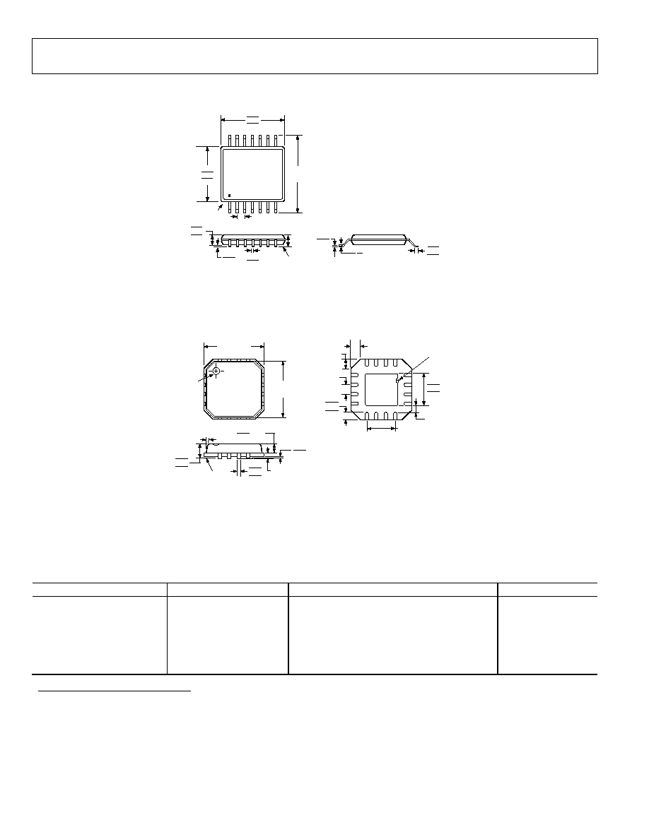
OUTLINE DIMENSIONS
4.50
4.40
4.30
14
8
7
1
6.40
BSC
PIN 1
5.10
5.00
4.90
0.65
BSC
SEATING
PLANE
0.15
0.05
0.30
0.19
1.20
MAX
1.05
1.00
0.80
0.20
0.09
8∞
0∞
0.75
0.60
0.45
COPLANARITY
0.10
COMPLIANT TO JEDEC STANDARDS MO-153AB-1
Figure 38. 14-Lead Thin Shrink Small Outline Package [TSSOP] (RU)
Dimensions shown in millimeters
16
5
13
8
9
12
1
4
BOTTOM
VIEW
2.25
2.10 SQ
1.95
0.75
0.60
0.50
0.65 BSC
1.95 BSC
0.35
0.28
0.25
12∞ MAX
0.20 REF
SEATING
PLANE
PIN 1
INDICATOR
TOP
VIEW
4.0
BSC SQ
3.75
BSC SQ
0.60 MAX
0.60 MAX
0.05 MAX
0.02 NOM
0.80 MAX
0.65 TYP
PIN 1
INDICATOR
1.00
0.85
0.80
COPLANARITY
0.08
0.25 MIN
COMPLIANT TO JEDEC STANDARDS MO-220-VGGC
Figure 39. 16-Terminal Leadless Frame Chip Scale Package [LFCSP] (CP)
Dimensions shown in millimeters
ORDERING GUIDE
Model
Temperature Range
Package Description
Package Option
ADD8704ARU
≠40∞C to +85∞C
14-Lead Thin Shrink SOIC
RU-14
ADD8704ARU-REEL
≠40∞C to +85∞C
14-Lead Thin Shrink SOIC
RU-14
ADD8704ARUZ
1
≠40∞C to +85∞C
14-Lead Thin Shrink SOIC
RU-14
ADD8704ARUZ-REEL
1
≠40∞C to +85∞C
14-Lead Thin Shrink SOIC
RU-14
ADD8704ACPZ-R2
1
≠40∞C to +85∞C
16-Terminal Leadless Frame Chip Scale
CP-16
ADD8704ACPZ-REEL7
1
≠40∞C to +85∞C
16-Terminal Leadless Frame Chip Scale
CP-16
1
Z = Pb-free part.

ADD8704
NOTES
Rev. 0 | Page 15 of 16

ADD8704
Rev. 0 | Page 16 of 16
NOTES
© 2003 Analog Devices, Inc. All rights reserved. Trademarks and
registered trademarks are the property of their respective owners.
C04417≠0≠10/03(0)