 | ÐлекÑÑоннÑй компоненÑ: ADG3247 | СкаÑаÑÑ:  PDF PDF  ZIP ZIP |
Äîêóìåíòàöèÿ è îïèñàíèÿ www.docs.chipfind.ru
Preliminary Technical Data
PRELIMINARY TECHNICAL DATA
REV. PrD
ADG3247
2.5 V/3.3 V, 16-Bit, 2-Port
Level Translating, Bus Switch
Information furnished by Analog Devices is believed to be accurate and
reliable. However, no responsibility is assumed by Analog Devices for its
use, nor for any infringements of patents or other rights of third parties that
may result from its use. No license is granted by implication or otherwise
under any patent or patent rights of Analog Devices. Trademarks and
registered trademarks are the property of their respective companies.
One Technology Way, P.O. Box 9106, Norwood, MA 02062-9106, U.S.A.
Tel: 781/329-4700
www.analog.com
Fax: 781/326-8703
© 2003 Analog Devices, Inc. All rights reserved.
FEATURES
225 ps Propagation Delay through the Switch
4.5 Switch Connection between Ports
Data Rate 1.244 Gbps
2.5 V/3.3 V Supply Operation
Selectable Level Shifting/Translation
Small Signal Bandwidth 610 MHz
Level Translation
3.3 V to 2.5 V
3.3 V to 1.8 V
2.5 V to 1.8 V
40-Lead 6 mm 6 mm LFCSP and 38-Lead TSSOP
Packages
APPLICATIONS
3.3 V to 1.8 V Voltage Translation
3.3 V to 2.5 V Voltage Translation
2.5 V to 1.8 V Voltage Translation
Bus Switching
Bus Isolation
Hot Plug
Hot Swap
Analog Switching Applications
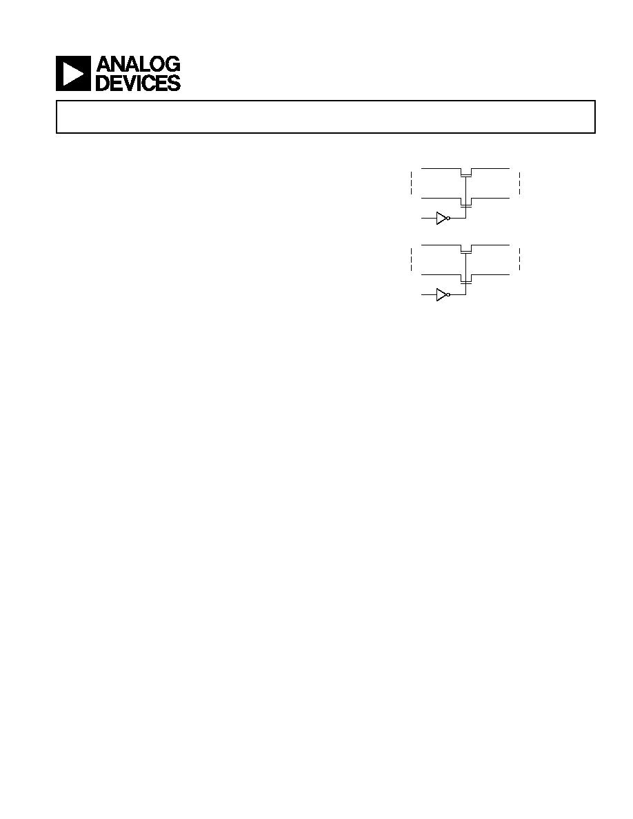
FUNCTIONAL BLOCK DIAGRAM
A7
B7
BE1
A0
B0
A15
B15
BE2
A8
B8
GENERAL DESCRIPTION
The ADG3247 is a 2.5 V or 3.3 V 16-bit, 2-port digital switch.
It is designed on Analog Devices' low voltage CMOS process,
which provides low power dissipation yet gives high switching
speed and very low on resistance, allowing inputs to be connected
to outputs without additional propagation delay or generating
additional ground bounce noise.
The ADG3247 is organized as dual 8-bit bus switches with
separate Bus Enable (
BEx) inputs. This allows the device to be
used as two 8-bit digital switches or one 16-bit bus switch. These
bus switches allow bidirectional signals to be switched when ON.
In the OFF condition, signal levels up to the supplies are blocked.
This device is ideal for applications requiring level translation.
When operated from a 3.3 V supply, level translation from 3.3 V
inputs to 2.5 V outputs occurs. Similarly, if the device is operated
from a 2.5 V supply and 2.5 V inputs are applied, the device will
translate the outputs to 1.8 V. In addition to this, the ADG3247
has a level translating select pin (
SEL). When SEL is low, V
CC
is
reduced internally, allowing for level translation between 3.3 V
inputs and 1.8 V outputs. This makes the device suited to appli-
cations requiring level translation between different supplies, such
as converter to DSP/microcontroller interfacing.
PRODUCT HIGHLIGHTS
1. 3.3 V or 2.5 V supply operation
2. Extremely low propagation delay through switch
3. 4.5
switches connect inputs to outputs
4. Level/voltage translation
5. 40-lead 6 mm 6 mm LFCSP and 38-lead TSSOP packages

PRELIMINARY TECHNICAL DATA
REV. PrD
2
ADG3247SPECIFICATIONS
1
(V
CC
= 2.3 V to 3.6 V, GND = 0 V, all specifications T
MIN
to T
MAX
, unless otherwise
noted.)
B Version
Parameter
Symbol
Conditions
Min
Typ
2
Max
Unit
DC ELECTRICAL CHARACTERISTICS
Input High Voltage
V
INH
V
CC
= 2.7 V to 3.6 V
2.0
V
V
INH
V
CC
= 2.3 V to 2.7 V
1.7
V
Input Low Voltage
V
INL
V
CC
= 2.7 V to 3.6 V
0.8
V
V
INL
V
CC
= 2.3 V to 2.7 V
0.7
V
Input Leakage Current
I
I
±0.01
±1
µA
OFF State Leakage Current
I
OZ
0 A, B V
CC
±0.01
±1
µA
ON State Leakage Current
I
OL
0 A, B V
CC
±0.01
±1
µA
Max Pass Voltage
V
P
V
A
/V
B
= V
CC
=
SEL = 3.3 V, I
O
= 5
µA
2.0
2.5
2.9
V
V
A
/V
B
= V
CC
=
SEL = 2.5 V, I
O
= 5
µA
1.5
1.8
2.1
V
V
A
/V
B
= V
CC
= 3.3 V,
SEL = 0 V, I
O
= 5
µA
1.5
1.8
2.1
V
CAPACITANCE
3
A Port Off Capacitance
C
A
OFF
f = 1 MHz
5
pF
B Port Off Capacitance
C
B
OFF
f = 1 MHz
5
pF
A, B Port On Capacitance
C
A
, C
B
ON f = 1 MHz
10
pF
Control Input Capacitance
C
IN
f = 1 MHz
6
pF
SWITCHING CHARACTERISTICS
3
Propagation Delay A to B or B to A,
t
PD
4
t
PHL,
t
PLH
C
L
= 50 pF, V
CC
=
SEL = 3 V
0.225
ns
Propagation Delay Matching
5
22.5
ps
Bus Enable Time
BEx to A or B
6
t
PZH
, t
PZL
V
CC
= 3.0 V to 3.6 V;
SEL = V
CC
1
3.2
4.8
ns
Bus Disable Time
BEx to A or B
6
t
PHZ
, t
PLZ
V
CC
= 3.0 V to 3.6 V;
SEL = V
CC
1
3.2
4.8
ns
Bus Enable Time
BEx to A or B
6
t
PZH
, t
PZL
V
CC
= 3.0 V to 3.6 V;
SEL = 0 V
0.5
2.2
3.3
ns
Bus Disable Time
BEx to A or B
6
t
PHZ
, t
PLZ
V
CC
= 3.0 V to 3.6 V;
SEL = 0 V
0.5
1.7
2.9
ns
Bus Enable Time
BEx to A or B
6
t
PZH
, t
PZL
V
CC
= 2.3 V to 2.7 V;
SEL = V
CC
0.5
2.2
3
ns
Bus Disable Time
BEx to A or B
6
t
PHZ
, t
PLZ
V
CC
= 2.3 V to 2.7 V;
SEL = V
CC
0.5
1.75
2.6
ns
Max Data Rate
V
CC
=
SEL = 3.3 V; V
A
/V
B
= 2 V
1.244
Gbps
Channel Jitter
V
CC
=
SEL = 3.3 V; V
A
/V
B
= 2 V
50
ps p-p
Operating Frequency--Bus Enable
f
BEx
10
MHz
DIGITAL SWITCH
On Resistance
R
ON
V
CC
= 3 V,
SEL = V
CC
, V
A
= 0 V, I
BA
= 8 mA
4.5
8
V
CC
= 3 V,
SEL = V
CC
, V
A
= 1.7 V, I
BA
= 8 mA
15
28
V
CC
= 2.3 V,
SEL = V
CC
, V
A
= 0 V, I
BA
= 8 mA
5
9
V
CC
= 2.3 V,
SEL = V
CC
, V
A
= 1 V, I
BA
= 8 mA
11
18
V
CC
= 3 V,
SEL = 0 V, V
A
= 0 V, I
BA
= 8 mA
5
8
V
CC
= 3 V,
SEL = 0 V, V
A
= 1 V, I
BA
= 8 mA
14
On Resistance Matching
R
ON
V
CC
= 3 V,
SEL = V
CC
, V
A
= 0 V, I
BA
= 8 mA
0.45
V
CC
= 3 V,
SEL = V
CC
, V
A
= 1 V, I
BA
= 8 mA
0.65
POWER REQUIREMENTS
V
CC
2.3
3.6
V
Quiescent Power Supply Current
I
CC
Digital Inputs = 0 V or V
CC
;
SEL = V
CC
0.001
1
µA
I
CC
Digital Inputs = 0 V or V
CC
;
SEL = 0 V
0.65
1.2
mA
Increase in I
CC
per Input
7
I
CC
V
CC
= 3.6 V,
BE
1
= 3.0 V;
BE
2
= V
CC
or GND;
SEL = V
CC
85
µA
NOTES
1
Temperature range is as follows: B Version: 40
°C to +85°C.
2
Typical values are at 25
°C, unless otherwise stated.
3
Guaranteed by design, not subject to production test.
4
The digital switch contributes no propagation delay other than the RC delay of the typical R
ON
of the switch and the load capacitance when driven by an ideal voltage
source. Since the time constant is much smaller than the rise/fall times of typical driving signals, it adds very little propagation delay to the system. Propagation delay
of the digital switch when used in a system is determined by the driving circuit on the driving side of the switch and its interaction with the load on the driven side.
5
Propagation delay matching between channels is calculated from the on resistance matching and load capacitance of 50 pF.
6
See Timing Measurement Information.
7
This current applies to the control pins (
BEx) only. The A and B ports contribute no significant ac or dc currents as they transition.
Specifications subject to change without notice.
PRELIMINARY TECHNICAL DATA
REV. PrD
ADG3247
3
ABSOLUTE MAXIMUM RATINGS
*
(T
A
= 25
°C, unless otherwise noted.)
V
CC
to GND . . . . . . . . . . . . . . . . . . . . . . . . . 0.5 V to +4.6 V
Digital Inputs to GND . . . . . . . . . . . . . . . . . 0.5 V to +4.6 V
DC Input Voltage . . . . . . . . . . . . . . . . . . . . . 0.5 V to +4.6 V
DC Output Current . . . . . . . . . . . . . . . . . . . . . . . . . . . 120 mA
Operating Temperature Range
Industrial (B Version) . . . . . . . . . . . . . . . . . 40
°C to +85°C
Storage Temperature Range . . . . . . . . . . . . 65
°C to +150°C
Junction Temperature . . . . . . . . . . . . . . . . . . . . . . . . . . 150
°C
LFCSP Package
JA
Thermal Impedance . . . . . . . . . . . . . . . . . . . . . . . 32
°C/W
TSSOP Package
JA
Thermal Impedance . . . . . . . . . . . . . . . . . . . . . 98
°C/W
Lead Temperature, Soldering (10 seconds) . . . . . . . . . . 300
°C
IR Reflow, Peak Temperature (<20 seconds) . . . . . . . . 235
°C
*Stresses above those listed under Absolute Maximum Ratings may cause perma-
nent damage to the device. This is a stress rating only; functional operation of the
device at these or any other conditions above those listed in the opera tional
sections of this specification is not implied. Exposure to absolute maximum rating
conditions for extended periods may affect device reliability. Only one absolute
maximum rating may be applied at any one time.
CAUTION
ESD (electrostatic discharge) sensitive device. Electrostatic charges as high as 4000 V readily
accumulate on the human body and test equipment and can discharge without detection. Although the
ADG3247 features proprietary ESD protection circuitry, permanent damage may occur on devices
subjected to high energy electrostatic discharges. Therefore, proper ESD precautions are recommended
to avoid performance degradation or loss of functionality.
Table I. Pin Description
Mnemonic
Description
BEx
Bus Enable (Active Low)
SEL
Level Translation Select
Ax
Port A, Inputs or Outputs
Bx
Port B, Inputs or Outputs
Table II. Truth Table
BEx SEL* Function
L
L
A = B, 3.3 V to 1.8 V Level Shifting
L
H
A = B, 3.3 V to 2.5 V/2.5V to 1.8 V Level Shifting
H
X
Disconnect
*SEL = 0 only when V
DD
= 3.3 V
± 10%
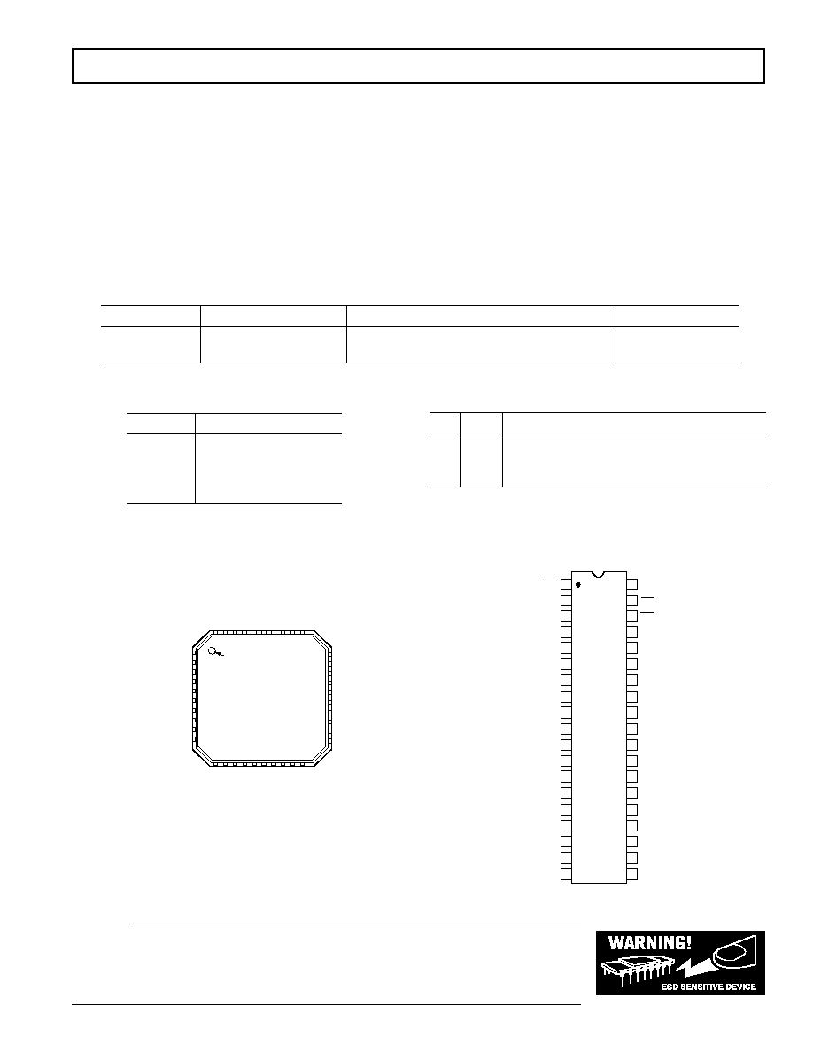
PIN CONFIGURATION
40-Lead LFCSP and 38-Lead TSSOP
PIN 1
INDICATOR
TOP VIEW
ADG3247
1
A6
2
A7
3
A8
4
A9
5
A10
6
A11
7
A12
8
A13
9
A14
10
A15
NC = NO CONNECT
GND 11
NC 12
NC 13
NC 14
B15 15
B14 1
6
B13 17
B12 18
B11 19
B10 20
30 B0
29 B1
28 B2
27 B3
26 B4
25 B5
24 B6
23 B7
22 B8
21 B9
40 A5
39 A4
38 A3
37 A2
36 A1
35 A0
34
SEL
33 VCC
32
BE2
31
BE1
TOP VIEW
(Not to Scale)
38
37
36
35
34
33
32
1
2
3
4
5
6
7
SEL
A0
A1
A2
A3
A4
A5
V
CC
BE2
BE1
B0
B1
B2
B3
ADG3247
31
30
29
8
9
10
A6
A7
A8
B4
B5
B6
28
27
11
12
A9
A10
B7
B8
26
25
A11
A12
B9
B10
24
23
22
17
A13
A14
A15
B11
B12
B13
21
20
18
19
GND
NC
B14
B15
13
14
15
16
ORDERING GUIDE
Model
Temperature Range
Package Description
Package Option
ADG3247BCP
40
°C to +85°C
Leaded Chip Scale Package (LFCSP)
CP-40
ADG3247BRU
40
°C to +85°C
Thin Shrink Small Outline Package (TSSOP)
RU-38

PRELIMINARY TECHNICAL DATA
REV. PrD
ADG3247
4
TERMINOLOGY
V
CC
Positive Power Supply Voltage
GND
Ground (0 V) Reference
V
INH
Minimum Input Voltage for Logic 1
V
INL
Maximum Input Voltage for Logic 0
I
I
Input Leakage Current at the Control Inputs
I
OZ
OFF State Leakage Current. It is the maximum leakage current at the switch pin in the OFF state.
I
OL
ON State Leakage Current. It is the maximum leakage current at the switch pin in the ON state.
V
P
Max Pass Voltage. The max pass voltage relates to the clamped output voltage of an NMOS device when the switch
input voltage is equal to the supply voltage.
R
ON
Ohmic Resistance Offered by a Switch in the ON State. It is measured at a given voltage by forcing a specified
amount of current through the switch.
R
ON
On Resistance Match between Any Two Channels, i.e., R
ON
Max R
ON
Min
C
X
OFF
OFF Switch Capacitance
C
X
ON
ON Switch Capacitance
C
IN
Control Input Capacitance. This consists of
BEx and SEL.
I
CC
Quiescent Power Supply Current. It is measured when all control inputs are at a logic HIGH or LOW level and
the switches are OFF.
I
CC
Extra Power Supply Current Component per each
BEx Control Input when the Input is not Driven at the Supplies.
t
PLH
, t
PHL
Data Propagation Delay through the Switch in the ON State. Propagation delay is related to the RC time constant
R
ON
C
L
, where C
L
is the load capacitance.
t
PZH
, t
PZL
Bus Enable Times. These are the times taken to cross the V
T
voltage at the switch output when the switch turns on
in response to the control signal,
BEx.
t
PHZ
, t
PLZ
Bus Disable Times. These are the times taken to place the switch in the high impedance OFF state in response to the
control signal. They are measured as the time taken for the output voltage to change by V from the original quiescent
level, with reference to the logic level transition at the control input. (Refer to Figure 3 for enable and disable times.)
Max Data Rate
Maximum Rate at which Data Can Be Passed through the Switch
Channel Jitter
Peak-to-Peak Value of the Sum of the Deterministic and Random Jitter of the Switch Channel
f
BE
Operating Frequency of Bus Enable. This is the maximum frequency at which Bus Enable (BE) can be toggled.
PRELIMINARY TECHNICAL DATA
REV. PrD
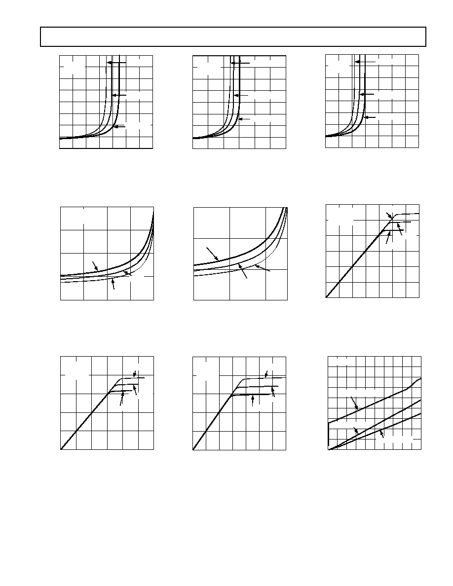
Typical Performance CharacteristicsADG3247
5
V
A
/V
B
V
R
ON
0
0
0.5
T
A
= 25 C
SEL = V
CC
5
10
15
20
25
30
35
40
1.5
2.5
3.5
V
CC
= 3V
V
CC
= 3.3V
V
CC
= 3.6V
3.0
2.0
1.0
TPC 1. On Resistance vs.
Input Voltage
V
A
/V
B
V
R
ON
0
0
0.5
5
10
15
20
1.5
2.0
1.0
25 C
85 C
40 C
= 3.3V
SEL = V
CC
V
CC
TPC 4. On Resistance vs. Input
Voltage for Different Temperatures
V
CC
V
V
OUT
V
0
0
0.5
0.5
1.5
2.5
1.5
2.5
V
CC
= 2.7V
V
CC
= 2.5V
V
CC
= 2.3V
T
A
= 25 C
SEL = V
CC
I
O
= 5 A
2.0
1.0
1.0
2.0
3.0
TPC 7. Pass Voltage vs. V
CC
V
A
/V
B
V
R
ON
0
0
0.5
5
10
15
20
25
30
35
40
1.5
2.5
V
CC
= 2.3V
V
CC
= 2.5V
V
CC
= 2.7V
T
A
= 25 C
SEL = V
CC
3.0
2.0
1.0
TPC 2. On Resistance vs.
Input Voltage
V
A
/V
B
V
R
ON
0
0
0.5
5
10
15
85 C
25 C
1.0
40 C
= 2.5V
SEL = V
CC
V
CC
1.2
TPC 5. On Resistance vs. Input
Voltage for Different Temperatures
V
CC
V
V
OUT
V
0
0
0.5
0.5
1.5
2.5
1.5
2.5
V
CC
= 3.6V
V
CC
= 3.3V
V
CC
= 3V
3.5
T
A
= 25 C
SEL = 0V
I
O
= 5 A
2.0
1.0
1.0
2.0
3.0
TPC 8. Pass Voltage vs. V
CC
V
A
/V
B
V
R
ON
0
0
0.5
5
10
15
20
25
30
35
40
1.5
2.5
V
CC
= 3V
V
CC
= 3.3V
V
CC
= 3.6V
3.5
T
A
= 25 C
SEL = 0V
1.0
2.0
3.0
TPC 3. On Resistance vs.
Input Voltage
V
CC
V
V
OUT
V
0
0
0.5
0.5
1.5
2.5
1.5
2.5
3.5
V
CC
= 3.6V
V
CC
= 3.3V
V
CC
= 3V
3.0
2.0
1.0
1.0
2.0
3.0
T
A
= 25 C
SEL = V
CC
I
O
= 5 A
TPC 6. Pass Voltage vs. V
CC
ENABLE FREQUENCY MHz
I
CC
A
0
0
2
4
200
6
8
10
T
A
= 25 C
12
V
CC
= 3.3V,
SEL = 0V
14 16
18 20
400
600
800
1000
1200
1400
1600
1800
V
CC
=
SEL = 3.3V
V
CC
=
SEL = 2.5V
TPC 9. I
CC
vs. Enable Frequency
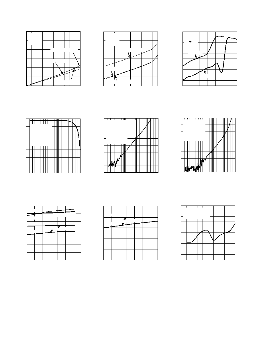
PRELIMINARY TECHNICAL DATA
REV. PrD
ADG3247
6
I
O
A
V
OUT
V
0
0.01
0.5
1.0
1.5
2.0
2.5
3.0
0.02 0.03 0.04 0.05 0.06 0.07 0.08 0.09 0.10
0
V
CC
= 3.3V;
SEL = 0V
V
CC
=
SEL = 3.3V
V
CC
=
SEL = 2.5V
T
A
= 25 C
V
A
= 0V
BE = 0
TPC 10. Output Low Characteristic
FREQUENCY MHz
A
TTENU
A
TION dB
0
0.03
0.1
1000
2
1
10
100
4
6
8
10
12
T
A
= 25 C
V
CC
= 3.3V/2.5V
SEL = V
CC
V
IN
= 0dBm
N/W ANALYZER :
R
L
= R
S
= 50
14
TPC 13. Bandwidth vs. Frequency
TEMPERATURE C
0
40
0.5
1.5
2.5
3.5
20
0
20
40
60
80
100
ENABLE
DISABLE
ENABLE
DISABLE
V
CC
=
SEL = 3.3V
V
CC
= 3.3V,
SEL = 0V
3.0
2.0
1.0
TIME ns
TPC 16. Enable/Disable Time
vs. Temperature
I
O
A
V
OUT
V
0
0.10
0.5
1.0
1.5
2.0
2.5
3.0
0
T
A
= 25 C
V
A
= V
CC
BE = 0
0.09 0.08 0.07 0.06 0.05 0.04 0.03 0.02 0.01
V
CC
=
SEL = 2.5V
V
CC
= 3.3V;
SEL = 0V
V
CC
=
SEL = 3.3V
TPC 11. Output High Characteristic
FREQUENCY MHz
A
TTENU
A
TION dB
0.03
0.1
1000
1
10
100
80
90
70
60
50
40
30
20
100
T
A
= 25 C
V
CC
= 3.3V/2.5V
SEL = V
CC
ADJACENT CHANNELS
V
IN
= 0dBm
N/W ANALYZER :
R
L
= R
S
= 50
TPC 14. Crosstalk vs. Frequency
TEMPERATURE C
TIME ns
0
40
0.5
1.5
2.5
20
0
20
40
60
80
100
ENABLE
DISABLE
V
CC
=
SEL = 2.5V
2.0
1.0
TPC 17. Enable/Disable Time
vs. Temperature
V
A
/V
B
V
Q
INJ
pC
2.0
0
0.5
1.0
0.2
1.5
2.5
0.4
0.6
0.8
1.2
1.4
1.8
1.0
2.0
3.0
1.6
0
V
CC
= 3.3V
V
CC
= 2.5V
T
A
= 25 C
SEL = V
CC
ON OFF
C
L
= InF
TPC 12. Charge Injection vs.
Source Voltage
FREQUENCY MHz
A
TTENU
A
TION dB
0.03
0.1
1000
1
10
100
80
90
70
60
50
40
30
20
T
A
= 25 C
V
CC
= 3.3V/2.5V
SEL = V
CC
V
IN
= 0dBm
N/W ANALYZER :
R
L
= R
S
= 50
100
TPC 15. Off Isolation vs.
Frequency
DATA RATE GBPS
JITTER ps
0.5 0.6
60
70
80
90
100
50
0.7 0.8 0.9
1.1 1.2 1.3 1.4 1.5
1.0
40
30
20
10
0
V
CC
=
SEL = 3.3V
V
IN
= 2V p-p
20dB ATTENUATION
TPC 18. Jitter vs. Data Rate;
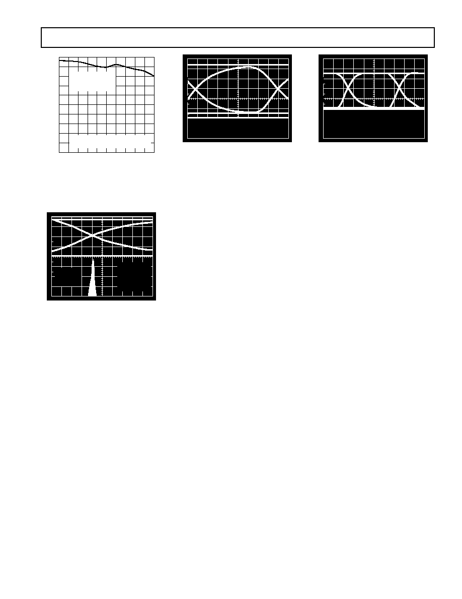
PRBS 31
PRELIMINARY TECHNICAL DATA
REV. PrD
ADG3247
7
DATA RATE GBPS
EYE WIDTH %
0.5 0.6
60
70
80
85
90
95
100
% EYE WIDTH = ((CLOCK PERIOD
JITTER p-p)/CLOCK PERIOD) 100%
75
65
55
50
0.7 0.8 0.9
1.1 1.2 1.3 1.4 1.5
1.0
V
CC
=
SEL = 3.3V
V
IN
= 2V p-p
20dB ATTENUATION
TPC 19. Eye Width vs. Data
Rate; PRBS 31
50.1mV/DIV
50ps/DIV
T
A
= 25 C
20dB
ATTENUATION
V
CC
= 3.3V
SEL = 3.3V
V
IN
= 2V p-p
TPC 22. Jitter @ 1.244 GBPS,
PRBS 31
V
CC
= 3.3V
SEL = 3.3V
V
IN
= 2V p-p
20dB
ATTENUATION
T
A
= 25 C
35mV/DIV
100ps/DIV
TPC 20. Eye Pattern; 1.244
GBPS, V
CC
= 3.3 V, PRBS 31
37mV/DIV
200ps/DIV
V
CC
= 2.5V
SEL = 2.5V
V
IN
= 2V p-p
20dB
ATTENUATION
T
A
= 28 C
TPC 21. Eye Pattern; 1 GBPS,
V
CC
= 2.5 V, PRBS 31
PRELIMINARY TECHNICAL DATA
REV. PrD
ADG3247
8
V
CC
V
IN
V
OUT
C
L
R
L
R
L
SW1
GND
OPEN
2 V
CC
R
T
D.U.T.
PULSE
GENERATOR
NOTES
PULSE GENERATOR FOR ALL PULSES:
t
R
2.5ns,
t
F
2.5ns,
FREQUENCY 10MHz.
C
L
INCLUDES BOARD, STRAY, AND LOAD CAPACITANCES.
R
T
IS THE TERMINATION RESISTOR, SHOULD BE EQUAL TO Z
OUT
OF THE PULSE GENERATOR.
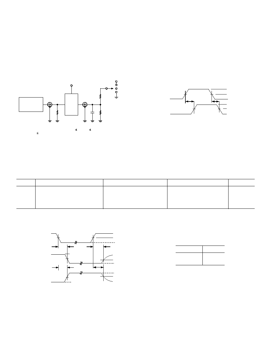
Figure 1. Load Circuit
SWITCH INPUT
0V
t
PHL
OUTPUT
V
T
V
IH
V
H
V
T
V
L
t
PLH
Figure 2. Propagation Delay
For the following load circuit and waveforms, the notation that is
used is V
IN
and V
OUT
where:
V
V and V
V
or
V
V and V
V
IN
A
OUT
B
IN
B
OUT
A
=
=
=
=
Test Conditions
Symbol
V
CC
= 3.3 V
±
0.3 V (
SEL =
V
CC
)
V
CC
= 2.5 V
±
0.2 V (
SEL =
V
CC
)
V
CC
= 3.3
V
±
0.3 V (
SEL = 0 V)
Unit
R
L
500
500
500
V
300
150
150
mV
C
L
50
30
30
pF
V
T
1.5
0.9
0.9
V
ENABLE
DISABLE
CONTROL INPUT
BEx
V
IN
= 0V
V
IN
= V
CC
V
OUT
SW1 @ 2V
CC
V
OUT
SW1 @ GND
t
PLZ
t
PZH
t
PHZ
t
PZL
V
T
0V
V
CC
V
T
V
H
V
H
V
V
L
V
L
+ V
V
CC
0V
V
T
V
INH
0V
Figure 3. Enable and Disable Times
TIMING MEASUREMENT INFORMATION
Table III. Switch Position
TEST
S1
t
PLZ
, t
PZL
2 V
CC
t
PHZ
, t
PZH
GND
PRELIMINARY TECHNICAL DATA
REV. PrD
ADG3247
9
BUS SWITCH APPLICATIONS
Mixed Voltage Operation, Level Translation
Bus switches can be used to provide an ideal solution for inter-
facing between mixed voltage systems. The ADG3247 is suitable
for applications where voltage translation from 3.3 V technology to
a lower voltage technology is needed. This device can translate
from 3.3 V to 1.8 V, from 2.5 V to 1.8 V, or bidirectionally from
3.3 V directly to 2.5 V.
Figure 4 shows a block diagram of a typical application in which a
user needs to interface between a 3.3 V ADC and a 2.5 V micro-
processor. The microprocessor may not have 3.3 V tolerant inputs;
therefore placing the ADG3247 between the two devices allows the
devices to communicate easily. The bus switch directly connects
the two blocks, thus introducing minimal propagation delay,
timing skew, or noise.
3.3V ADC
2.5V
3.3V
2.5V
MICROPROCESSOR
ADG3247
3.3V
Figure 4. Level Translation between a 3.3 V ADC
and a 2.5 V Microprocessor
3.3 V to 2.5 V Translation
When V
CC
is 3.3 V (
SEL = V
CC
) and the input signal range is 0 V
to V
CC
, the maximum output signal will be clamped to within
a voltage threshold below the V
CC
supply.
ADG3247
2.5V
2.5V
3.3V
2.5V
3.3V
Figure 5. 3.3 V to 2.5 V Voltage Translation,
SEL = V
CC
In this case, the output will be limited to 2.5 V, as shown in
Figure 6.
V
IN
2.5V
V
OUT
0V
3.3V
SWITCH
INPUT
S
WITCH
OU
TPUT
3.3V SUPPLY
SEL = 3.3V
Figure 6. 3.3 V to 2.5 V Voltage Translation,
SEL = V
CC
This device can be used for translation from 2.5 V to 3.3 V
devices, and also between two 3.3 V devices.
2.5 V to 1.8 V Translation
When V
CC
is 2.5 V (
SEL = V
CC
) and the input signal range is 0 V
to V
CC
, the maximum output signal will, as before, be clamped
to within a voltage threshold below the V
CC
supply.
ADG3247
1.8V
2.5V
2.5V
Figure 7. 2.5 V to 1.8 V Voltage Translation,
SEL = V
CC
In this case, the output will be limited to approximately 1.8 V,
as shown in Figure 7.
V
IN
1.8V
V
OUT
0V
2.5V
SWITCH
INPUT
S
WITCH
OU
TPUT
2.5V SUPPLY
SEL = 2.5V
Figure 8. 2.5 V to 1.8 V Voltage Translation,
SEL = V
CC
3.3 V to 1.8 V Translation
The ADG3247 offers the option of interfacing between a 3.3 V
device and a 1.8 V device. This is possible through use of the
SEL pin.
SEL pin: An active low control pin. SEL activates internal
circuitry in the ADG3247 that allows voltage translation between
3.3 V devices and 1.8 V devices.
ADG3247
1.8V
3.3V
3.3V
Figure 9. 3.3 V to 1.8 V Voltage Translation,
SEL = 0 V
When V
CC
is 3.3 V and the input signal range is 0 V to V
CC
, the
maximum output signal will be clamped to 1.8 V, as shown in
Figure 9. To do this, the
SEL pin must be tied to Logic 0. If
SEL is unused, it should be tied directly to V
CC
.
PRELIMINARY TECHNICAL DATA
REV. PrD
ADG3247
10
V
IN
1.8V
V
OUT
0V
3.3V
SWITCH
INPUT
S
WITCH
OU
TPUT
3.3V SUPPLY
SEL = 0V
Figure 10. 3.3 V to 1.8 V Voltage Translation,
SEL = 0 V
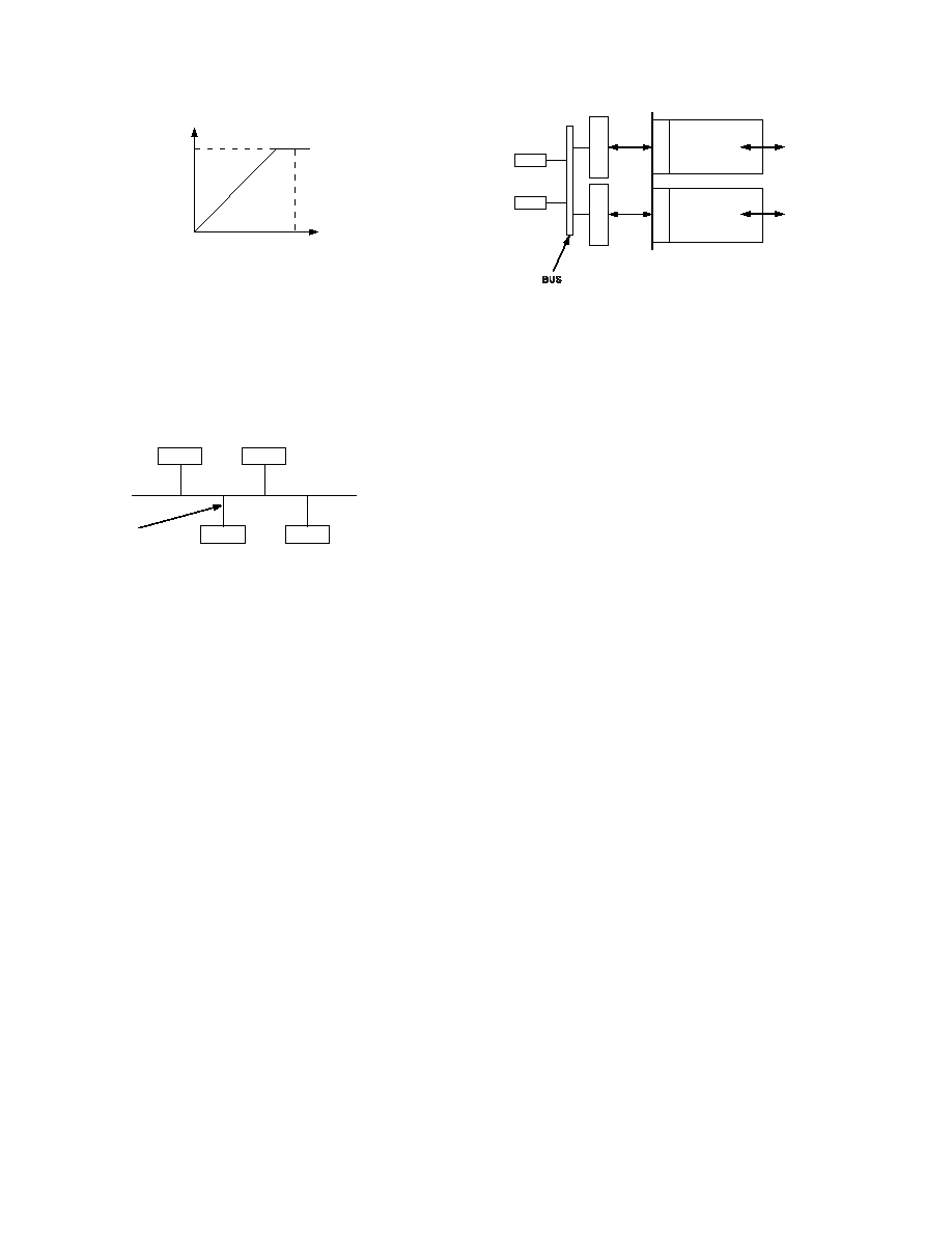
Bus Isolation
A common requirement of bus architectures is low capacitance
loading of the bus. Such systems require bus bridge devices that
extend the number of loads on the bus without exceeding the
specifications. Because the ADG3247 is designed specifically for
applications that do not need drive yet require simple logic func-
tions, it solves this requirement. The device isolates access to the
bus, thus minimizing capacitance loading.
Bus/
Backplane
Load A
Load C
Load B
Load D
Bus Switch
Location
Figure 11. Location of Bus Switched in a Bus
Isolation Application
Hot Plug and Hot Swap Isolation
The ADG3247 is suitable for hot swap and hot plug applications.
The output signal of the ADG3247 is limited to a voltage that is
below the V
CC
supply, as shown in Figures 6, 8, and 10. There-
fore the switch acts like a buffer to take the impact from hot
insertion, protecting vital and expensive chipsets from damage.
In hot-plug applications, the system cannot be shutdown when
new hardware is being added. To overcome this, a bus switch can
be positioned on the backplane between the bus devices and the
hot plug connectors. The bus switch is turned off during hot plug.
Figure 12 shows a typical example of this type of application.
PLUG-IN
CARD (1)
CARD I/O
CARD I/O
RAM
CPU
PLUG-IN
CARD (2)
ADG3247
ADG3247
Figure 12. ADG3247 in a Hot Plug Application
There are many systems that require the ability to handle hot
swapping, such as docking stations, PCI boards for servers, and
line cards for telecommunications switches. If the bus can be
isolated prior to insertion or removal, then there is more control
over the hot swap event. This isolation can be achieved using a
bus switch. The bus switches are positioned on the hot swap card
between the connector and the devices. During hot swap, the
ground pin of the hot swap card must connect to the ground pin
of the back plane before any other signal or power pins.
Analog Switching
Bus switches can be used in many analog switching applications;
for example, video graphics. Bus switches can have lower on
resistance, smaller ON and OFF channel capacitance and thus
improved frequency performance than their analog counterparts.
The bus switch channel itself consisting solely of an NMOS
switch limits the operating voltage (see TPC 1 for a typical plot),
but in many cases this does not present an issue.
High Impedance during Power-Up/Power-Down
To ensure the high impedance state during power-up or power-
down, BEx should be tied to V
CC
through a pull-up resistor; the
minimum value of the resistor is determined by the current-
sinking capability of the driver.
PACKAGE AND PINOUT
The ADG3247 is packaged in both a small 38-lead TSSOP or a
tiny 40-lead LFCSP package. The area of the TSSOP option is
62.7 mm
2
, while the area of the LFCSP option is 36 mm
2
. This
leads to a 43% savings in board space when using the LFCSP
package compared with the TSSOP package. This makes the LFCSP
option an excellent choice for space-constrained applications.
The ADG3247 in the TSSOP package offers a flowthrough
pinout. The term flowthrough signifies that all the inputs are on
opposite sides from the outputs. A flowthrough pinout simplifies
the PCB layout.
PRELIMINARY TECHNICAL DATA
REV. PrD
ADG3247
11
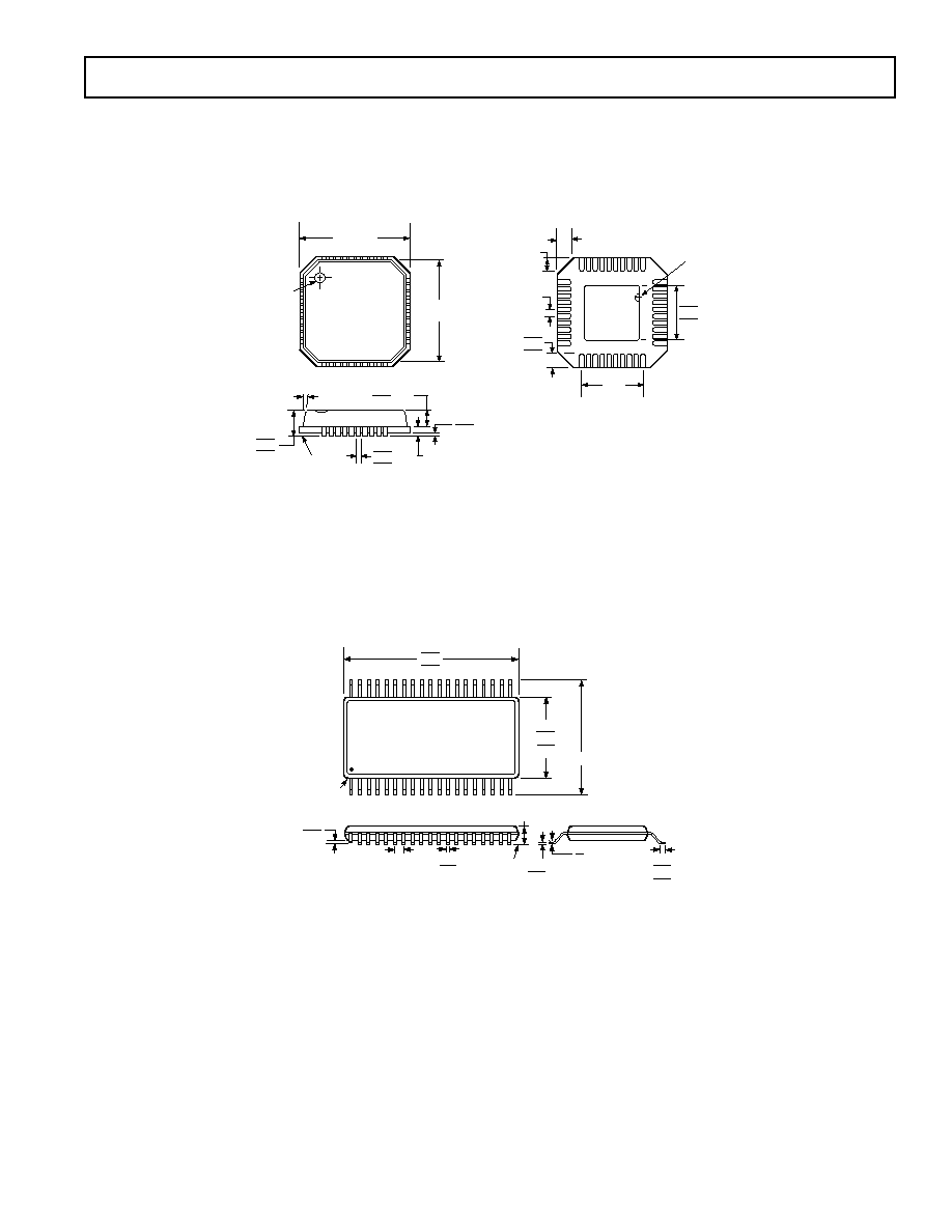
OUTLINE DIMENSIONS
40-Lead Frame Chip Scale Package [LFCSP]
(CP-40)
Dimensions shown in millimeters
1
40
10
11
31
30
21
20
BOTTOM
VIEW
4.25
3.70 SQ
1.75
TOP
VIEW
6.00
BSC SQ
PIN 1
INDICATOR
5.75
BSC SQ
12
MAX
0.30
0.23
0.18
0.20 REF
SEATING
PLANE
1.00
0.90
0.80
0.05 MAX
0.02 NOM
COPLANARITY
0.08
1.00 MAX
0.65 NOM
4.50
REF
0.50
0.40
0.30
0.50
BSC
PIN 1
INDICATOR
0.60 MAX
0.60 MAX
COMPLIANT TO JEDEC STANDARDS MO-220-VJJD-2
38-Lead Thin Shrink Small Outline Package [TSSOP]
(RU-38)
Dimensions shown in millimeters
38
20
19
1
9.80
9.70
9.60
PIN 1
SEATING
PLANE
0.15
0.05
0.50
BSC
1.20
MAX
0.27
0.17
0.20
0.09
8
0
4.50
4.40
4.30
6.40 BSC
0.70
0.60
0.45
COMPLIANT TO JEDEC STANDARDS MO-153BD-1
COPLANARITY
0.10

C0301302/03(PrD)
PRINTED IN U.S.A.
12