 | ÐлекÑÑоннÑй компоненÑ: ADG3257 | СкаÑаÑÑ:  PDF PDF  ZIP ZIP |
Äîêóìåíòàöèÿ è îïèñàíèÿ www.docs.chipfind.ru
a
ADG3257
Information furnished by Analog Devices is believed to be accurate and
reliable. However, no responsibility is assumed by Analog Devices for its
use, nor for any infringements of patents or other rights of third parties that
may result from its use. No license is granted by implication or otherwise
under any patent or patent rights of Analog Devices. Trademarks and
registered trademarks are the property of their respective companies.
One Technology Way, P.O. Box 9106, Norwood, MA 02062-9106, U.S.A.
Tel: 781/329-4700
www.analog.com
Fax: 781/326-8703
© 2003 Analog Devices, Inc. All rights reserved.
REV. C
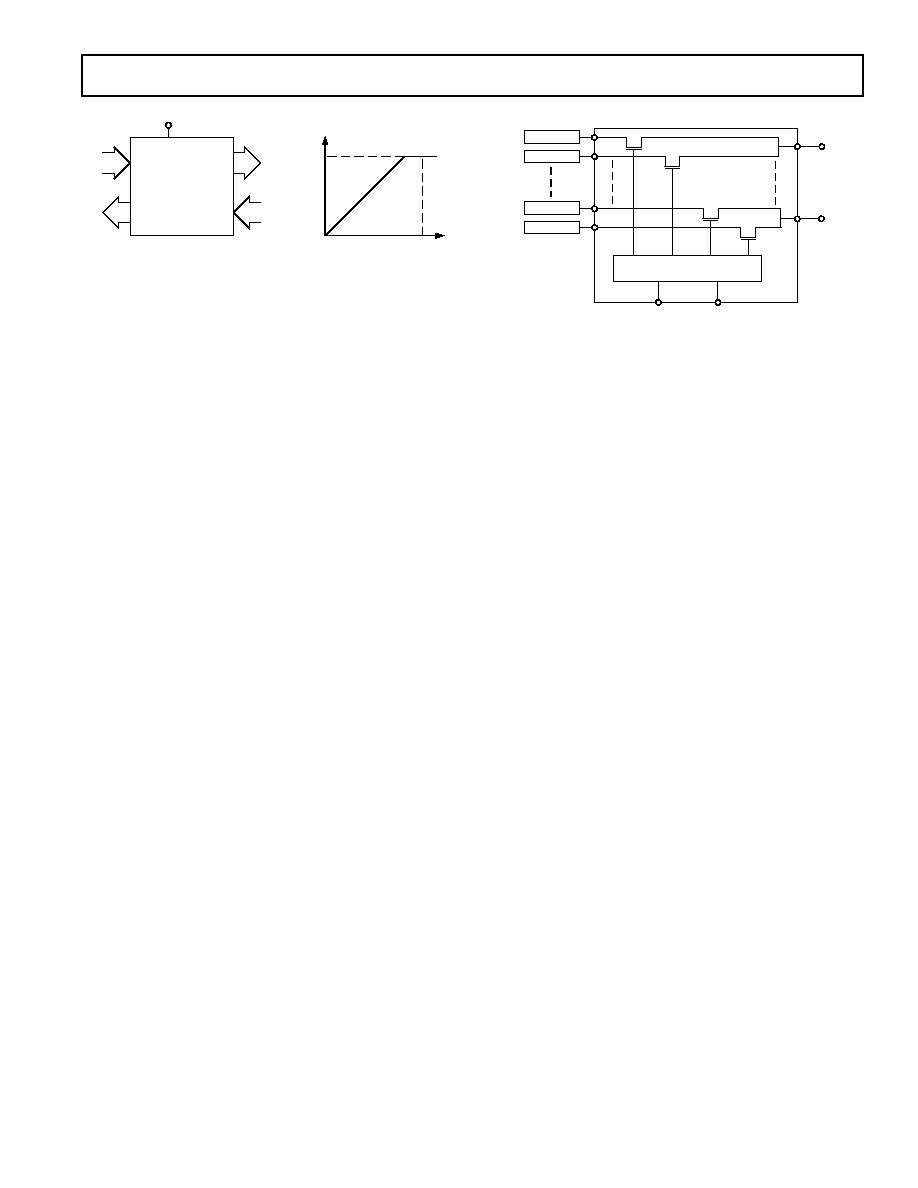
High Speed, 3.3 V/5 V Quad 2:1 Mux/Demux
(4-Bit, 1 of 2) Bus Switch
FUNCTIONAL BLOCK DIAGRAM
1A
2A
3A
4A
4B
2
4B
1
3B
2
3B
1
2B
2
2B
1
1B
2
1B
1
BE
S
LOGIC
FEATURES
100 ps Propagation Delay through the Switch
2
Switches Connect Inputs to Outputs
Data Rates up to 933 Mbps
Single 3.3 V/5 V Supply Operation
Level Translation Operation
Ultralow Quiescent Supply Current (1 nA Typical)
3.5 ns Switching
Standard `3257 Type Pinout
APPLICATIONS
Bus Switching
Bus Isolation
Level Translation
Memory Switching/Interleaving
PRODUCT HIGHLIGHTS
1. 0.1 ns propagation delay through switch
2. 2
switches connect inputs to outputs
3. Bidirectional operation
4. Ultralow power dissipation
5. 16-lead QSOP package
Table I. Truth Table
BE
S
Function
H
X
DISABLE
L
L
A = B
1
L
H
A = B
2
GENERAL DESCRIPTION
The ADG3257 is a CMOS bus switch comprised of four 2:1
multiplexers/demultiplexers with high impedance outputs. The
device is manufactured on a CMOS process. This provides low
power dissipation yet high switching speed and very low ON
resistance, allowing the inputs to be connected to the outputs
without adding propagation delay or generating additional ground
bounce noise.
The ADG3257 operates from a single 3.3 V/5 V supply. The
control logic for each switch is shown in Table I. These switches
are bidirectional when ON. In the OFF condition, signal levels are
blocked up to the supplies.
This bus switch is suited to both switching and level translation
applications. It may be used in applications requiring level
translation from 3.3 V to 2.5 V when powered from 3.3 V.
Additionally, with a diode connected in series with 5 V V
DD
,
the ADG3257 may also be used in applications requiring 5 V
to 3.3 V level translation.

REV. C
2
ADG3257SPECIFICATIONS
1
(V
CC
= 5.0 V 10%, GND = 0 V. All specifications T
MIN
to T
MAX
, unless otherwise noted.)
B Version
Parameter
Symbol
Conditions
2
Min
Typ
3
Max
Unit
DC ELECTRICAL CHARACTERISTICS
Input High Voltage
V
INH
2.4
V
Input Low Voltage
V
INL
0.3
+0.8
V
Input Leakage Current
I
I
0 V
IN
5.5 V
±0.01 ± 1
µA
OFF State Leakage Current
I
OZ
0 A, B V
CC
±0.01 ± 1
µA
ON State Leakage Current
I
OZ
0 A, B V
CC
±0.01 ± 1
µA
Max Pass Voltage
4
V
P
V
IN
= V
CC
= 5 V, I
O
= 5
µA
3.9
4.2
4.4
V
CAPACITANCE
4
A Port OFF Capacitance
C
A
OFF
f = 1 MHz
7
pF
B Port OFF Capacitance
C
B
OFF
f = 1 MHz
5
pF
A, B Port ON Capacitance
C
A
, C
B
ON
f = 1 MHz
11
pF
Control Input Capacitance
C
IN
f = 1 MHz
4
pF
SWITCHING CHARACTERISTICS
4
Propagation Delay A to B or B to A
t
PD
t
PHL
,
t
PLH
5
V
A
= 0 V, C
L
= 50 pF
0.10
ns
Propagation Delay Matching
6
V
A
= 0 V, C
L
= 50 pF
0.0075 0.035 ns
Bus Enable Time
BE to A or B
t
PZH
, t
PZL
C
L
= 50 pF, R
L
= 500
1
5
7.5
ns
Bus Disable Time
BE to A or B
t
PHZ
, t
PLZ
C
L
= 50 pF, R
L
= 500
1
3.5
7
ns
Bus Select Time S to A or B
Enable
t
SEL_EN
C
L
= 50 pF, R
L
= 500
8
12
ns
Disable
t
SEL_DIS
C
L
= 50 pF, R
L
= 500
5
8
ns
Max Data Rate
V
A
= 2 V p-p
933
Mbps
DIGITAL SWITCH
ON Resistance
R
ON
V
A
= 0 V
I
O
= 48 mA, 15 mA, 8 mA, T
A
= 25
°C
2
3
I
O
= 48 mA, 15 mA, 8 mA
4
V
A
= 2.4 V
I
O
= 48 mA, 15 mA, 8 mA, T
A
= 25
°C
3
5
I
O
= 48 mA, 15 mA, 8 mA
6
ON Resistance Matching
R
ON
V
A
= 0 V
48 mA, 15 mA, 8 mA, T
A
= 25
°C
0.15
0.35
V
A
= 0 V, 48 mA, 15 mA, 8 mA
0.7
POWER REQUIREMENTS
V
CC
3.0
5.5
V
Quiescent Power Supply Current
I
CC
Digital Inputs = 0 V or V
CC
0.001
1
µA
Increase in I
CC
per Input
7
I
CC
V
CC
= 5.5 V, One Input at 3.0 V;
Others at V
CC
or GND
200
µA
NOTES
1
Temperature range is as follows: B Version: 40
°C to +85°C.
2
See Test Circuits and Waveforms.
3
All typical values are at T
A
= 25
°C, unless otherwise noted.
4
Guaranteed by design, not subject to production test.
5
The digital switch contributes no propagation delay other than the RC delay of the typical R
ON
of the switch and the load capacitance when driven by an ideal voltage
source. Since the time constant is much smaller than the rise/fall times of typical driving signals, it adds very little propagation delay to the system. Propagation delay
of the digital switch when used in a system is determined by the driving circuit on the driving side of the switch and its interaction with the load on the driven side.
6
Propagation delay matching between channels is calculated from ON resistance matching of worst-case channel combinations and load capacitance.
7
This current applies to the control pins only and represents the current required to switch internal capacitance at the specified frequency. The A and B ports
contribute no significant ac or dc currents as they transition. This parameter is guaranteed by design, not subject to production test.
Specifications subject to change without notice.

REV. C
3
ADG3257
SPECIFICATIONS
1
(V
CC
= 3.3 V 10%, GND = 0 V. All specifications T
MIN
to T
MAX
, unless otherwise noted.)
B Version
Parameter
Symbol
Conditions
2
Min
Typ
3
Max
Unit
DC ELECTRICAL CHARACTERISTICS
Input High Voltage
V
INH
2.0
V
Input Low Voltage
V
INL
0.3
+0.8
V
Input Leakage Current
I
I
0 V
IN
3.6 V
±0.01 ± 1
µA
OFF State Leakage Current
I
OZ
0 A, B V
CC
±0.01 ± 1
µA
ON State Leakage Current
I
OZ
0 A, B V
CC
±0.01 ± 1
µA
Max Pass Voltage
4
V
P
V
IN
= V
CC
= 3.3 V, I
O
= 5
µA
2.3
2.6
2.8
V
CAPACITANCE
4
A Port OFF Capacitance
C
A
OFF
f = 1 MHz
7
pF
B Port OFF Capacitance
C
B
OFF
f = 1 MHz
5
pF
A, B Port ON Capacitance
C
A
, C
B
ON f = 1 MHz
11
pF
Control Input Capacitance
C
IN
f = 1 MHz
4
pF
SWITCHING CHARACTERISTICS
4
Propagation Delay A to B or B to A
t
PD
t
PHL
,
t
PLH
5
V
A
= 0 V, C
L
= 50 pF
0.10
ns
Propagation Delay Matching
6
V
A
= 0 V, C
L
= 50 pF
0.01
0.04
ns
Bus Enable Time
BE to A or B
t
PZH
, t
PZL
C
L
= 50 pF, R
L
= 500
1
5.5
9
ns
Bus Disable Time
BE to A or B
t
PHZ
, t
PLZ
C
L
= 50 pF, R
L
= 500
1
4.5
8.5
ns
Bus Select Time S to A or B
Enable
t
SEL_EN
C
L
= 50 pF, R
L
= 500
8
12
ns
Disable
t
SEL_DIS
C
L
= 50 pF, R
L
= 500
6
9
ns
Max Data Rate
V
A
= 2 Vp-p
933
Mbps
DIGITAL SWITCH
ON Resistance
R
ON
V
A
= 0 V
I
O
= 15 mA, 8 mA, T
A
= 25
°C
2
4
4.5
V
A
= 1.7 V, I
O
= 15 mA, T
A
= 25
°C
8
16.5
18
V
A
= 1.7 V, I
O
= 8 mA, T
A
= 25
°C
7
14
17
ON Resistance Matching
R
ON
V
A
= 0 V, 15 mA, 8 mA, T
A
= 25
°C
0.2
0.4
V
A
= 0 V, 15 mA, 8 mA
0.8
POWER REQUIREMENTS
V
CC
3.0
5.5
V
Quiescent Power Supply Current
I
CC
Digital Inputs = 0 V or V
CC
0.001 1
µA
Increase in I
CC
per Input
7
I
CC
V
CC
= 3.3 V, One Input at 3.0 V;
Others at V
CC
or GND
200
µA
NOTES
1
Temperature range is as follows: B Version: 40
°C to +85°C.
2
See Test Circuits and Waveforms.
3
All typical values are at T
A
= 25
°C, unless otherwise noted.
4
Guaranteed by design, not subject to production test.
5
The digital switch contributes no propagation delay other than the RC delay of the typical R
ON
of the switch and the load capacitance when driven by an ideal voltage
source. Since the time constant is much smaller than the rise/fall times of typical driving signals, it adds very little propagation delay to the system. Propagation delay
of the digital switch when used in a system is determined by the driving circuit on the driving side of the switch and its interaction with the load on the driven side.
6
Propagation delay matching between channels is calculated from ON resistance matching of worst-case channel combinations and load capacitance.
7
This current applies to the control pins only and represents the current required to switch internal capacitance at the specified frequency. The A and B ports
contribute no significant ac or dc currents as they transition. This parameter is guaranteed by design, not subject to production test.
Specifications subject to change without notice.
REV. C
ADG3257
4
CAUTION
ESD (electrostatic discharge) sensitive device. Electrostatic charges as high as 4000 V readily
accumulate on the human body and test equipment and can discharge without detection. Although
the ADG3257 features proprietary ESD protection circuitry, permanent damage may occur on
devices subjected to high energy electrostatic discharges. Therefore, proper ESD precautions are
recommended to avoid performance degradation or loss of functionality.
WARNING!
ESD SENSITIVE DEVICE
ABSOLUTE MAXIMUM RATINGS
*
(T
A
= 25
°C, unless otherwise noted.)
V
CC
to GND . . . . . . . . . . . . . . . . . . . . . . . . . . 0.3 V to +6 V
Digital Inputs
to GND . . . . . . . . . . . . . . . . . . . 0.3 V to +6 V
DC Input Voltage . . . . . . . . . . . . . . . . . . . . . . 0.3 V to +6 V
DC Output Current . . . . . . . . . . . . . . . . . . . . . . . . . . 100 mA
Operating Temperature Range
Industrial (B Version) . . . . . . . . . . . . . . . . 40
°C to +85°C
Storage Temperature Range . . . . . . . . . . . . 65
°C to +150°C
Junction Temperature . . . . . . . . . . . . . . . . . . . . . . . . . 150
°C
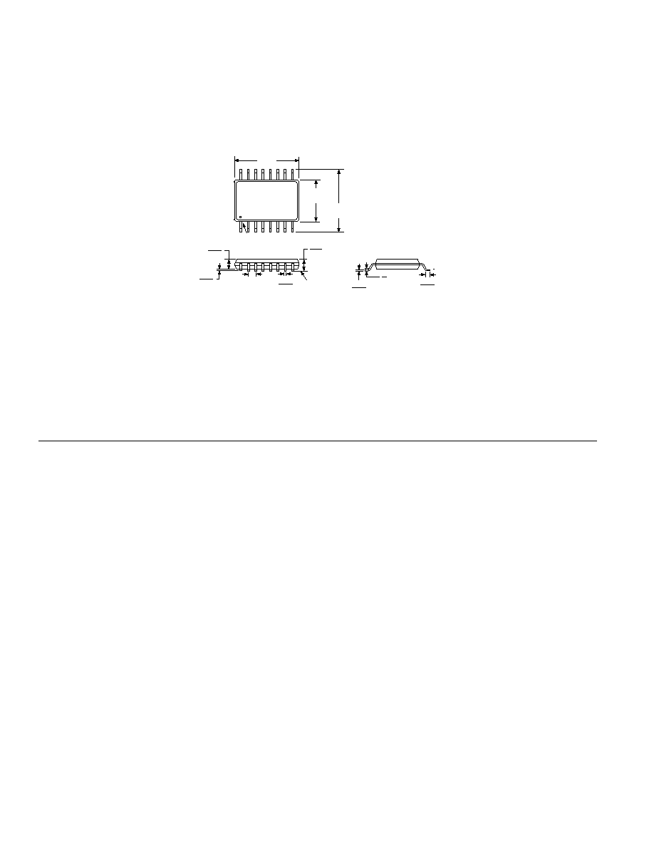
QSOP Package
JA
Thermal Impedance . . . . . . . . . . . . . . . . . . 149.97
°C/W
Lead Temperature, Soldering (10 sec) . . . . . . . . . . . . 300
°C
IR Reflow, Peak Temperature (<20 sec) . . . . . . . . . . . 235
°C
*Stresses above those listed under Absolute Maximum Ratings may cause perma-
nent damage to the device. This is a stress rating only and functional operation of
the device at these or any other conditions above those listed in the operational
sections of this specification is not implied. Exposure to absolute maximum rating
conditions for extended periods may affect device reliability. Only one absolute
maximum rating may be applied at any one time.
PIN CONFIGURATION
TOP VIEW
(Not to Scale)
16
15
14
13
12
11
10
9
1
2
3
4
5
6
7
8
S
1B
1
1B
2
1A
2B
1
2B
2
2A
GND
V
CC
BE
4B
1
4B
2
4A
3B
1
3B
2
3A
ADG3257
ORDERING GUIDE
Model
Temperature Range
Package Descriptions
Package Option
ADG3257BRQ
40
°C to +85°C
RQ = 0.15" Quarter Size Outline Package (QSOP)
RQ-16
PIN FUNCTION DESCRIPTIONS
Mnemonic
Description
BE
Output Enable (Active Low)
S
Port Select
Ax
Port A, Inputs or Outputs
Bx
Port B, Inputs or Outputs
REV. C
5
Typical Performance CharacteristicsADG3257
VA/VB V
R
ON
12
8
0
0
1
2
3
4
5
4
16
20
V
CC
= 4.5V
V
CC
= 5.0V
V
CC
= 5.5V
T
A
= 25 C
TPC 1. ON Resistance vs. Input
Voltage
VA/VB V
R
ON
10
0
0
0.5
5
15
20
V
CC
= 3V
+85 C
+25 C
40 C
1.0
1.5
2.0
2.5
3.0
TPC 4. ON Resistance vs. Input
Voltage for Different Temperatures
INPUT VOLTAGE V
OUTPUT VOLTAGE V
0
3.6
3
2
1
0
0.5
1.0
1.5
2.5
3.5
3.0
2.0
T
A
= 25 C
V
CC
= 3.6V
V
CC
= 3.3V
V
CC
= 3.0V
TPC 7. Max Pass Voltage
VA/VB V
R
ON
12
8
0
0
0.5
4
16
20
V
CC
= 2.7V
V
CC
= 3.0V
V
CC
= 3.3V
T
A
= 25 C
1.0
1.5
2.0
2.5
3.0
TPC 2. ON Resistance vs. Input
Voltage
V
CC
= 5V
T
A
= 25 C
FREQUENCY kHz
10m
0.1
CURRENT A
1m
100
10
1
100n
10n
1
10
100
1000
10000
V
CC
= 3V
TPC 5. I
CC
vs. Enable Frequency
20dB ATTENUATION
T
A
= 25 C
40mV/DIV
267ps/DIV
V
CC
= 5V
V
IN
= 2V p-p
622MBPS
TPC 8. 622 Mbps Eye Diagram
VA/VB V
R
ON
10
0
0
1
2
3
4
5
5
15
20
V
CC
= 5V
+85 C
40 C
+25 C
TPC 3. ON Resistance vs. Input
Voltage for Different Temperatures
INPUT VOLTAGE V
OUTPUT VOLTAGE V
0
5
4
3
2
1
0
1
2
3
4
5
V
CC
= 5.5V
V
CC
= 4.5V
V
CC
= 5.0V
T
A
= 25 C
TPC 6. Max Pass Voltage
20dB ATTENUATION
T
A
= 25 C
40mV/DIV
180ps/DIV
V
CC
= 5V
V
IN
= 2V p-p
933MBPS
TPC 9. 933 Mbps Eye Diagram
REV. C
ADG3257
6
D.U.T.
PULSE
1
GENERATOR
S1
V
CC
2
V
CC
OPEN
GND
C
L
2
V
IN
R
T
3
V
OUT
R
L
R
L
NOTES
1
PULSE GENERATOR FOR ALL PULSES:
t
F
< 2.5ns,
t
R
< 2.5ns.
2
C
L
= INCLUDES BOARD, STRAY, AND LOAD CAPACITANCES.
3
R
T
IS THE TERMINATION RESISTOR; SHOULD BE EQUAL TO Z
OUT
OF THE PULSE GENERATOR.
Figure 1. Load Circuit
SWITCH INPUT
OUTPUT
V
IH
V
T
0V
V
OH
V
T
V
OL
t
PLH
t
PHL
Figure 2. Propagation Delay
CONTROL INPUTS
V
IH
V
T
0V
V
OH
t
PZL
V
OH
V
0V
V
OL
V
OL
+ V
V
CC
V
T
0V
V
T
V
CC
OUTPUT
t
PLZ
t
PHZ
t
PZH
S1 @ 2 V
CC
LOW
S1 @ 2 V
CC
OUTPUT
ENABLE
DISABLE
Figure 3. Select, Enable, and Disable Times
Table II. Switch S1 Condition
Test
S1
t
PLH
, t
PHL
OPEN
t
PLZ
, t
PZL
2
× V
CC
t
PHZ
, t
PZH
GND
t
SEL
OPEN
Table III. Test Conditions
Symbol
V
CC
= 5 V
10%
V
CC
= 3.3 V
10%
Unit
R
L
500
500
V
300
300
mV
C
L
50
50
pF
APPLICATIONS
Mixed Voltage Operation, Level Translation
Bus switches can be used to provide a solution for mixed voltage
systems where interfacing bidirectionally between 5 V and 3 V
devices is required. To interface between 5 V and 3.3 V buses,
an external diode is placed in series with the 5 V power supply
as shown in Figure 4.
V
CC
= 5V
BE
3.3V TO 5V
3.3V TO 3.3V
5V MEMORY
5V I/O
3.3V CPU/DSP/
MICROPROCESSOR/
MEMORY
Figure 4. Level Translation Between 5 V and 3.3 V Devices
The diode drops the internal gate voltage down to 4.3 V.
The bus switch limits the voltage present on the output to
V
CC
external diode drop = V
TH
.
Therefore, assuming a diode drop of 0.7 V and a V
TH
of 1 V,
the output voltage would be limited to 3.3 V with a logic high.
V
IN
3.3V
V
OUT
5V SUPPLY
0V
5V
SWITCH INPUT
S
WITCH OUTPUT
Figure 5. Input Voltage to Output Voltage
Similarly, the device could be used to translate bidirectionally
between 3.3 V to 2.5 V systems. In this case, there is no need
for an external diode. The internal V
TH
drop is 1 V, so with a
V
CC
= 3.3 V the bus switch will limit the output voltage to
V
CC
1 V = 2.3 V.
REV. C
ADG3257
7
ADG3257
2.5V
2.5V
3.3V
2.5V
3.3V
V
IN
2.5V
V
OUT
3.3V SUPPLY
0V
3.3V
SWITCH INPUT
S
WITCH OUTPUT
Figure 6. 3.3 V to 2.5 V Level Translation Using the
ADG3257 Bus Switch
Memory Switching
This quad bus switch may be used to allow switching between
different memory banks, thus allowing additional memory and
decreasing capacitive loading. Figure 7 illustrates the ADG3257
in such an application.
SDRAM #1
SDRAM #2
BE
S
LOGIC
SDRAM #7
SDRAM #8
Figure 7. Allows Additional Memory Modules without
Added Drive or Delay
REV. C
8
C0291404/03(C)
ADG3257
Revision History
Location
Page
4/03--Data Sheet changed from REV. B to REV. C.
Updated Publication Code . . . . . . . . . . . . . . . . . . . . . . . . . . . . . . . . . . . . . . . . . . . . . . . . . . . . . . . . . . . . . . . . . . . . . . . . . . . . . . . . 8
4/03--Data Sheet changed from REV. A to REV. B.
Updated OUTLINE DIMENSIONS . . . . . . . . . . . . . . . . . . . . . . . . . . . . . . . . . . . . . . . . . . . . . . . . . . . . . . . . . . . . . . . . . . . . . . . . 8
06/02--Data Sheet changed from REV. 0 to REV. A.
Edits to FEATURES . . . . . . . . . . . . . . . . . . . . . . . . . . . . . . . . . . . . . . . . . . . . . . . . . . . . . . . . . . . . . . . . . . . . . . . . . . . . . . . . . . . . . 1
OUTLINE DIMENSIONS
16-Lead Shrink Small Outline Package [QSOP]
(RQ-16)
Dimensions shown in inches
16
9
8
1
PIN 1
SEATING
PLANE
0.010
0.004
0.012
0.008
0.025
BSC
0.010
0.006
0.050
0.016
8
0
COPLANARITY
0.004
0.065
0.049
0.069
0.053
0.154
BSC
0.236
BSC
COMPLIANT TO JEDEC STANDARDS MO-137AB
0.193
BSC
Document Outline
- FEATURES
- APPLICATIONS
- GENERAL DESCRIPTION
- FUNCTIONAL BLOCK DIAGRAM
- PRODUCT HIGHLIGHTS
- SPECIFICATIONS
- ABSOLUTE MAXIMUM RATINGS*
- PIN CONFIGURATION
- PIN FUNCTION DESCRIPTIONS
- ORDERING GUIDE
- Typical Performance Characteristics
- APPLICATIONS
- Mixed Voltage Operation, Level Translation
- Memory Switching
- OUTLINE DIMENSIONS
- REVISION HISTORY