 | ÐлекÑÑоннÑй компоненÑ: ADG333ABR | СкаÑаÑÑ:  PDF PDF  ZIP ZIP |
Äîêóìåíòàöèÿ è îïèñàíèÿ www.docs.chipfind.ru
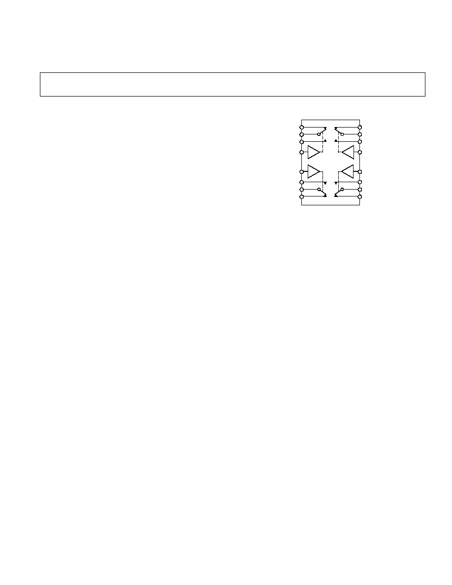
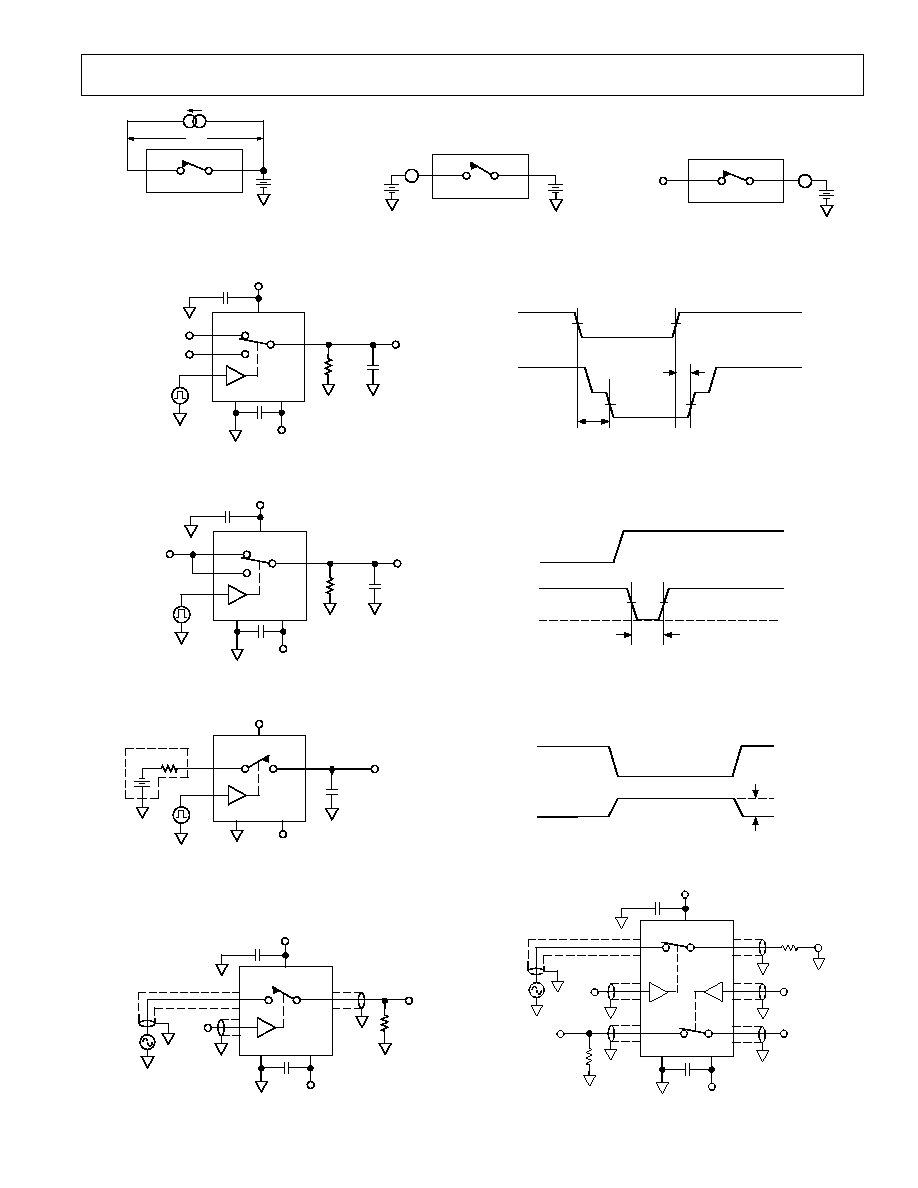
FUNCTIONAL BLOCK DIAGRAM
S1A
D1
S1B
IN1
IN2
S2B
D2
S2A
S3A
D3
S3B
IN3
IN4
S4B
D2
S4A
ADG333A
SWITCHES SHOWN FOR A LOGIC "1" INPUT
REV. 0
Information furnished by Analog Devices is believed to be accurate and
reliable. However, no responsibility is assumed by Analog Devices for its
use, nor for any infringements of patents or other rights of third parties
which may result from its use. No license is granted by implication or
otherwise under any patent or patent rights of Analog Devices.
a
Quad SPDT Switch
ADG333A
© Analog Devices, Inc., 1995
One Technology Way, P.O. Box 9106, Norwood, MA 02062-9106, U.S.A.
Tel: 617/329-4700
Fax: 617/326-8703
FEATURES
44 V Supply Maximum Ratings
V
SS
to V
DD
Analog Signal Range
Low On Resistance (45 max)
Low
R
ON
(5 max)
Low R
ON
Match (4 max)
Low Power Dissipation
Fast Switching Times
t
ON
< 175 ns
t
OFF
< 145 ns
Low Leakage Currents (5 nA max)
Low Charge Injection (10 pC max)
Break-Before-Make Switching Action
APPLICATIONS
Audio and Video Switching
Battery Powered Systems
Test Equipment
Communication Systems
GENERAL DESCRIPTION
The ADG333A is a monolithic CMOS device comprising four
independently selectable SPDT switches. It is designed on an
LC
2
MOS process which provides low power dissipation yet
achieves a high switching speed and a low on resistance.
The on resistance profile is very flat over the full analog input
range ensuring good linearity and low distortion when switching
audio signals. High switching speed also makes the part suitable
for video signal switching. CMOS construction ensures ultralow
power dissipation making the part ideally suited for portable,
battery powered instruments.
When they are ON, each switch conducts equally well in both
directions and has an input signal range which extends to the
power supplies. In the OFF condition, signal levels up to the
supplies are blocked. All switches exhibit break-before-make
switching action for use in multiplexer applications. Inherent in
the design is low charge injection for minimum transients when
switching the digital inputs.
PRODUCT HIGHLIGHTS
1. Extended Signal Range
The ADG333A is fabricated on an enhanced LC
2
MOS
process, giving an increased signal range which extends
to the supply rails.
2. Low Power Dissipation
3. Low R
ON
4. Single Supply Operation
For applications where the analog signal is unipolar,
the ADG333A can be operated from a single rail power
supply. The part is fully specified with a single +12 V
supply.

ADG333ASPECIFICATIONS
1
DUAL SUPPLY
40 C to
Parameter
+25 C
+85 C
Units
Test Conditions/Comments
ANALOG SWITCH
Analog Signal Range
V
SS
to V
DD
V
R
ON
20
typ
V
D
=
±
10 V, I
S
= 1 mA
45
45
max
R
ON
5
max
V
D
=
±
5 V, I
S
= 10 mA
R
ON
Match
4
max
V
D
=
±
10 V, I
S
= 10 mA
LEAKAGE CURRENTS
V
DD
= +16.5 V, V
SS
= 16.5 V
Source OFF Leakage I
S
(OFF)
±
0.1
nA typ
V
D
=
±
15.5 V, V
S
= +15.5 V
±
0.25
±
3
nA max
Test Circuit 2
Channel ON Leakage I
D
, I
S
(ON)
±
0.1
nA typ
V
S
= V
D
=
±
15.5 V
±
0.4
±
5
nA max
Test Circuit 3
DIGITAL INPUTS
Input High Voltage, V
INH
2.4
V min
Input Low Voltage, V
INL
0.8
V max
Input Current
I
INL
or I
INH
±
0.005
µ
A typ
V
IN
= 0 V or V
DD
±
0.5
µ
A max
DYNAMIC CHARACTERISTICS
2
t
ON
90
ns typ
R
L
= 300
, C
L
= 35 pF;
175
ns max
V
S
=
±
10 V; Test Circuit 4
t
OFF
80
ns typ
R
L
= 300
, C
L
= 35 pF;
145
ns max
V
S
=
±
10 V; Test Circuit 4
Break-Before-Make Delay, t
OPEN
10
ns min
R
L
= 300
, C
L
= 35 pF;
V
S
= +5 V; Test Circuit 5
Charge Injection
2
pC typ
V
D
= 0 V, R
D
= 0
, C
L
= 10 nF;
10
pC max
V
DD
= +15 V, V
SS
= 15 V; Test Circuit 6
OFF Isolation
72
dB typ
R
L
= 75
, C
L
= 5 pF, f = 1 MHz;
V
S
= 2.3 V
rms, Test Circuit 7
Channel-to-Channel Crosstalk
85
dB typ
R
L
= 75
, C
L
= 5 pF, f = 1 MHz;
V
S
= 2.3 V rms,
Test Circuit 8
C
S
(OFF)
5
pF typ
C
D
, C
S
(ON)
20
pF typ
POWER REQUIREMENTS
I
DD
0.05
mA typ
Digital Inputs = 0 V or 5 V
0.25
0.35
mA max
I
SS
0.01
µ
A typ
1
5
µ
A max
V
DD
/V
SS
±
3/
±
20
V min/V max |V
DD
| = |V
SS
|
NOTES
1
Temperature range is as follows: B Version: 40
°
C to +85
°
C.
2
Guaranteed by design, not subject to production test.
Specifications subject to change without notice.
REV. 0
2
(V
DD
= +15 V, V
SS
= 15 V, GND = 0 V, unless otherwise noted)

SINGLE SUPPLY
40 C to
Parameter
+25 C
+85 C
Units
Test Conditions/Comments
ANALOG SWITCH
Analog Signal Range
0 to V
DD
V
R
ON
35
typ
V
D
= +1 V, +10 V, I
S
= 1 mA
75
max
LEAKAGE CURRENTS
V
DD
= +13.2 V
Source OFF Leakage I
S
(OFF)
±
0.1
nA typ
V
D
= 12.2 V/1 V, V
S
= 1 V/12.2 V
±
0.25
±
3
nA max
Test Circuit 2
Channel ON Leakage I
D
, I
S
(ON)
±
0.1
nA typ
V
S
= V
D
= 12.2 V/1 V
±
0.4
±
5
nA max
Test Circuit 3
DIGITAL INPUTS
Input High Voltage, V
INH
2.4
V min
Input Low Voltage, V
INL
0.8
V max
Input Current
I
INL
or I
INH
±
0.005
µ
A typ
V
IN
= 0 V or V
DD
±
0.5
µ
A max
DYNAMIC CHARACTERISTICS
2
t
ON
110
ns typ
R
L
= 300
, C
L
= 35 pF;
200
ns max
V
S
= +8 V; Test Circuit 4
t
OFF
100
ns typ
R
L
= 300
, C
L
= 35 pF;
180
ns max
V
S
= +8 V; Test Circuit 4
Break-Before-Make Delay, t
OPEN
10
ns min
R
L
= 300
, C
L
= 35 pF;
ns min
V
S
= +5 V; Test Circuit 5
Charge Injection
5
pC typ
V
D
= 6 V, R
D
= 0
, C
L
= 10 nF;
V
DD
= +12 V, V
SS
= 0 V; Test Circuit 6
OFF Isolation
72
dB typ
R
L
= 75
, C
L
= 5 pF, f = 1 MHz;
V
S
= 1.15 V rms, Test Circuit 7
Channel-to-Channel Crosstalk
85
dB typ
R
L
= 75
, C
L
= 5 pF, f = 1 MHz;
V
S
= 1.15 V rms,
Test Circuit 8
C
S
(OFF)
5
pF typ
C
D
, C
S
(ON)
20
pF typ
POWER REQUIREMENTS
V
DD
= +13.5 V
I
DD
0.05
mA typ
Digital Inputs = 0 V or 5 V
0.25
0.35
mA max
V
DD
+3/+30
V min/V max
NOTES
1
Temperature range is as follows: B Version: 40
°
C to +85
°
C.
2
Guaranteed by design, not subject to production test.
Specifications subject to change without notice.
ADG333A
REV. 0
3
(V
DD
= +12 V, V
SS
= 0 V 10%, GND = 0 V, unless otherwise noted)
ADG333A
REV. 0
4
ABSOLUTE MAXIMUM RATINGS
1
(T
A
= +25
°
C unless otherwise noted)
V
DD
to V
SS
. . . . . . . . . . . . . . . . . . . . . . . . . . . . . . . . . . . +44 V
V
DD
to GND . . . . . . . . . . . . . . . . . . . . . . . . . 0.3 V to +30 V
V
SS
to GND . . . . . . . . . . . . . . . . . . . . . . . . . . +0.3 V to 30 V
Analog, Digital Inputs
2
. . . . . . . . . . . . V
SS
2 V to V
DD
+ 2 V
. . . . . . . . . . . . . . . . . . . . . .
or 20 mA, Whichever Occurs First
Continuous Current, S or D . . . . . . . . . . . . . . . . . . . . 20 mA
Peak Current, S or D . . . . . . . . . . . . . . . . . . . . . . . . . . 40 mA
(Pulsed at 1 ms, 10% Duty Cycle Max)
Operating Temperature Range
Industrial (B Version) . . . . . . . . . . . . . . . . 40
°
C to +85
°
C
Storage Temperature Range . . . . . . . . . . . . 65
°
C to +125
°
C
Junction Temperature . . . . . . . . . . . . . . . . . . . . . . . . +150
°
C
Plastic Package
JA
, Thermal Impedance . . . . . . . . . . . . . . . . . . . . 103
°
C/W
Lead Temperature, Soldering (10 sec) . . . . . . . . . . +260
°
C
SOIC Package
JA
, Thermal Impedance . . . . . . . . . . . . . . . . . . . . . 74
°
C/W
Lead Temperature, Soldering
Vapor Phase (60 sec) . . . . . . . . . . . . . . . . . . . . . . +215
°
C
Infrared (15 sec) . . . . . . . . . . . . . . . . . . . . . . . . . . +220
°
C
SSOP Package
JA
, Thermal Impedance . . . . . . . . . . . . . . . . . . . . 130
°
C/W
Lead Temperature, Soldering
Vapor Phase (60 sec) . . . . . . . . . . . . . . . . . . . . . . +215
°
C
Infrared (15 sec) . . . . . . . . . . . . . . . . . . . . . . . . . . +220
°
C
NOTES
1
Stresses above those listed under "Absolute Maximum Ratings" may cause
permanent damage to the device. This is a stress rating only and functional
operation of the device at these or any other conditions above those listed in the
operational sections of this specification is not implied. Exposure to absolute
maximum rating conditions for extended periods may affect device reliability.
Only one absolute maximum rating may be applied at any one time.
2
Overvoltages at IN, S or D will be clamped by internal diodes. Current should be
limited to the maximum ratings given.
WARNING!
ESD SENSITIVE DEVICE
CAUTION
ESD (electrostatic discharge) sensitive device. Electrostatic charges as high as 4000 V readily
accumulate on the human body and test equipment and can discharge without detection.
Although the ADG333A features proprietary ESD protection circuitry, permanent damage may
occur on devices subjected to high energy electrostatic discharges. Therefore, proper ESD
precautions are recommended to avoid performance degradation or loss of functionality.
ORDERING GUIDE
Model
Temperature Range
Package Option*
ADG333ABN
40
°
C to +85
°
C
N-20
ADG333ABR
40
°
C to +85
°
C
R-20
ADG333ABRS
40
°
C to +85
°
C
RS-20
*N = Plastic DIP, R = Small Outline IC (SOIC). RS = Shrink Small Outline
Package (SSOP).
Table I. Truth Table
Logic
Switch A
Switch B
0
OFF
ON
1
ON
OFF
ADG333A
REV. 0
5
TERMINOLOGY
S
Source Terminal. May be an input or output.
D
Drain Terminal. May be an input or output.
IN
Logic Control Input.
R
ON
Ohmic resistance between D and S.
R
ON
R
ON
variation due to a change in the analog
input voltage with a constant load current.
R
ON
Match
Difference between the R
ON
of any two
channels.
I
S
(OFF)
Source leakage current with the switch
"OFF."
I
D
(OFF)
Drain leakage current with the switch
"OFF."
I
D
, I
S
(ON)
Channel leakage current with the switch
"ON."
V
D
(V
S
)
Analog voltage on terminals D, S.
C
S
(OFF)
"OFF" Switch Source Capacitance.
C
D
(OFF)
"OFF" Switch Drain Capacitance.
C
D
, C
S
(ON)
"ON" Switch Capacitance.
t
ON
Delay between applying the digital control in-
put and the output switching on.
t
OFF
Delay between applying the digital control in-
put and the output switching off.
t
OPEN
Break Before Make delay when switches are
configured as a multiplexer.
V
INL
Maximum input voltage for logic "0."
V
INH
Minimum input voltage for logic "1."
I
INL
(I
INH
)
Input current of the digital input.
Crosstalk
A measure of unwanted signal which is
coupled through from one channel to another
as a result of parasitic capacitance.
Off Isolation
A measure of unwanted signal coupling
through an "OFF" switch.
Charge Injection A measure of the glitch impulse transferred
from the digital input to the analog output
during switching.
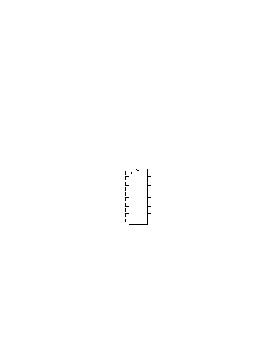
PIN CONFIGURATION
DIP/SOIC/SSOP
14
13
12
11
17
16
15
19
18
20
10
9
8
1
2
3
4
7
6
5
TOP VIEW
(Not to Scale)
ADG333A
NC = NO CONNECT
IN1
S4B
D4
S4A
IN4
S1A
D1
S1B
S3B
NC
V
DD
V
SS
GND
S2B
D2
S2A
IN2
IN3
S3A
D3
V
D
, V
S
Volts
R
ON
60
50
10
15
10
15
5
0
5
10
40
30
20
V
DD
= +5V
V
SS
= 5V
V
DD
= +10V
V
SS
= 10V
V
DD
= +15V
V
SS
= 15V
T
A
= +25
°
C
Figure 1. R
ON
as a Function of V
D
(V
S
): Dual Supply
V
D
, V
S
Volts
R
ON
100
90
20
0
3
15
6
9
12
60
50
40
30
80
70
T
A
= +25
°
C
V
DD
= +10V
V
SS
= 0V
V
DD
= +5V
V
SS
= 0V
V
DD
= +15V
V
SS
= 0V
Figure 2. R
ON
as a Function of V
D
(V
S
):
Single Power Supply
45
10
15
10
15
5
0
5
10
40
35
30
20
15
25
V
D
, V
S
Volts
R
ON
V
DD
= +15V
V
SS
= 15V
+125
°
C
+85
°
C
+25
°
C
40
°
C
Figure 3. R
ON
as a Function of V
D
(V
S
)
for Different Temperatures: Dual
Supply
60
50
10
0
3
15
6
9
12
40
30
20
V
D
, V
S
Volts
R
ON
V
DD
= +15V
V
SS
= 0V
+125
°
C
+85
°
C
40
°
C
+25
°
C
Figure 4. R
ON
as a Function of V
D
(V
S
)
for Different Temperatures: Single
Supply
0.004
0.01
15
10
15
5
0
5
10
LEAKAGE CURRENT nA
0.002
0
0.002
0.006
0.008
0.004
V
D
, V
S
Volts
V
DD
= +16.5V
V
SS
= 16.5V
T
A
= +25
°
C
I
S
(OFF)
I
D
(ON)
I
S
(ON)
Figure 5. Leakage Currents as a
Function of V
D
(V
S
): Dual Supply
0.001
0
0.004
0
3
12
6
9
0.001
0.002
0.003
LEAKAGE CURRENT nA
V
D
, V
S
Volts
V
DD
= +16.5V
V
SS
= 16.5V
T
A
= +25
°
C
I
S
(OFF)
I
D
(ON)
I
S
(ON)
Figure 6. Leakage Currents as a
Function of V
D
(V
S
): Single Supply
V
S
Volts
Q pC
20
20
15
0
5
10
15
10
5
15
10
15
5
0
5
10
V
DD
= +16.5V
V
SS
= 16.5V
V
DD
= +12V
V
SS
= 0V
C
L
= 10nF
Figure 7. Charge Injection as a
Function of V
S
SWITCHING TIME ns
160
140
60
0
5
20
10
15
120
100
80
V
DD
Volts
V
D
= +2V
V
S
= 2V
Figure 8. Switching Time as a
Function of V
DD
SWITCHING FREQUENCY kHz
I
DD
mA
1
0.8
0
0
200
1000
400
600
800
0.6
0.4
0.2
V
DD
= +16.5V
V
SS
= 16.5V
T
A
= +25
°
C
Figure 9. I
DD
as a Function of
Switching Frequency
ADG333ATypical Performance Graphs
6
REV. 0
ADG333A
REV. 0
7
S
D
V
IN1
S
D
75
V
IN2
NC
20 x LOG
|
V
S
/ V
OUT
|
CHANNEL TO CHANNEL
CROSSTALK
R
L
75
V
OUT
GND
V
SS
V
DD
V
DD
0.1µF
0.1µF
V
SS
V
S
Test Circuit 8. Channel-to-Channel Crosstalk
S
D
GND
V
SS
V
DD
V
DD
V
OUT
0.1µF
R
L
75
0.1µF
V
SS
V
IN
V
S
Test Circuit 7. Off Isolation
V
D
S
D
A
I
D
(ON)
NC
Test Circuit 3. On Leakage
D
GND
V
SS
0.1µF
V
SS
IN
SA
SB
V
DD
10V
+10V
V
S
V
DD
0.1µF
V
OUT
C
L
35pF
R
L
300
50%
t
OFF
50%
50%
50%
t
ON
V
IN
V
S
3V
0V
+10V
0V
10V
Test Circuit 4. Switching Times
D
GND
V
SS
0.1µF
V
SS
IN
SA
SB
V
DD
V
S
V
DD
0.1µF
V
OUT
C
L
35pF
R
L
300
t
OPEN
3V
0V
V
IN
V
OUT
V
S
50%
50%
Test Circuit 5. Break-Before-Make Delay, t
OPEN
V
D
R
D
GND
V
SS
V
SS
IN
V
DD
V
DD
V
OUT
C
L
10nF
D
SA
Q
INJ
= C
L
x
V
OUT
V
IN
V
OUT
3V
0V
0V
V
OUT
Test Circuit 6. Charge Injection
V
D
I
DS
S
D
R
ON
= V
1
/I
DS
V
1
Test Circuit 1. On Resistance
V
D
S
D
A
V
S
I
S
(OFF)
Test Circuit 2. Off Leakage
ADG333A
REV. 0
8
PRINTED IN U.S.A.
C20761810/95
APPLICATIONS INFORMATION
ADG333A Supply Voltages
The ADG333A can operate off a dual or signal supply. V
SS
should be connected to GND when operating with a single
supply. When using a dual supply the ADG333A can also oper-
ate with unbalanced supplies, for example V
DD
= 20 V and V
SS
= 5 V. The only restrictions are that V
DD
to GND must not
exceed 30 V, V
SS
to GND must not drop below 30 V and V
DD
to V
SS
must not exceed +44 V. It is important to remember that
the ADG333A supply voltage directly affects the input signal
range, the switch ON resistance and the switching times of the
part. The effects of the power supplies on these characteristics
can be clearly seen from the characteristic curves in this data
sheet.
Power Supply Sequencing
When using CMOS devices care must be taken to ensure
correct power-supply sequencing. Incorrect power-supply
sequencing can result in the device being subjected to stresses
beyond those maximum ratings listed in the data sheet. This is
also true for the ADG333A. Always sequence V
DD
on first
followed by V
SS
and the logic signals. An external signal within
the maximum specified ratings can then be safely presented to
the source or drain of the switch
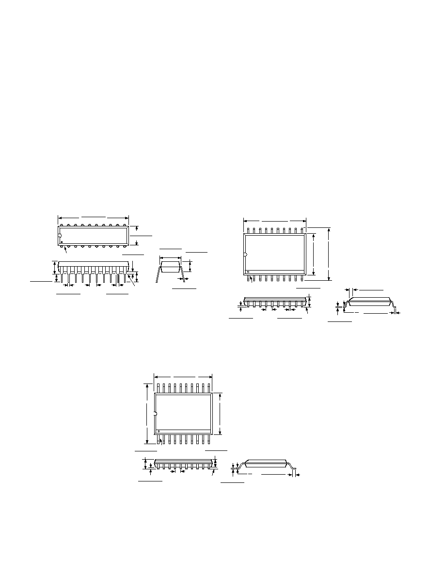
OUTLINE DIMENSIONS
Dimensions shown in inches and (mm).
20-Pin Plastic DIP (N-20)
20
1
10
11
1.060 (26.90)
0.925 (23.50)
0.280 (7.11)
0.240 (6.10)
PIN 1
SEATING
PLANE
0.022 (0.558)
0.014 (0.356)
0.060 (1.52)
0.015 (0.38)
0.210 (5.33)
MAX
0.130
(3.30)
MIN
0.070 (1.77)
0.045 (1.15)
0.100
(2.54)
BSC
0.160 (4.06)
0.115 (2.93)
0.325 (8.25)
0.300 (7.62)
0.015 (0.381)
0.008 (0.204)
0.195 (4.95)
0.115 (2.93)
20-Pin SOIC (R-20)
SEATING
PLANE
0.0118 (0.30)
0.0040 (0.10)
0.0192 (0.49)
0.0138 (0.35)
0.1043 (2.65)
0.0926 (2.35)
0.0500
(1.27)
BSC
0.0125 (0.32)
0.0091 (0.23)
0.0500 (1.27)
0.0157 (0.40)
8
°
0
°
0.0291 (0.74)
0.0098 (0.25)
x 45
°
20
11
10
1
0.5118 (13.00)
0.4961 (12.60)
0.4193 (10.65)
0.3937 (10.00)
0.2992 (7.60)
0.2914 (7.40)
PIN 1
20-Pin SSOP (RS-20)
20
11
10
1
0.295 (7.50)
0.271 (6.90)
0.311 (7.9)
0.301 (7.64)
0.212 (5.38)
0.205 (5.21)
PIN 1
SEATING
PLANE
0.008 (0.203)
0.002 (0.050)
0.07 (1.78)
0.066 (1.67)
0.0256
(0.65)
BSC
0.078 (1.98)
0.068 (1.73)
0.009 (0.229)
0.005 (0.127)
0.037 (0.94)
0.022 (0.559)
8
°
0
°
LEADS WILL BE EITHER TIN PLATED OR SOLDIER DIPPED
IN ACCORDANCE WITH MIL-M-38510 REQUIREMENTS