 | ÐлекÑÑоннÑй компоненÑ: ADG467 | СкаÑаÑÑ:  PDF PDF  ZIP ZIP |
Äîêóìåíòàöèÿ è îïèñàíèÿ www.docs.chipfind.ru
REV. A
Information furnished by Analog Devices is believed to be accurate and
reliable. However, no responsibility is assumed by Analog Devices for its
use, nor for any infringements of patents or other rights of third parties
which may result from its use. No license is granted by implication or
otherwise under any patent or patent rights of Analog Devices.
a
ADG466/ADG467
One Technology Way, P.O. Box 9106, Norwood, MA 02062-9106, U.S.A.
Tel: 781/329-4700
World Wide Web Site: http://www.analog.com
Fax: 781/326-8703
© Analog Devices, Inc., 1998
Triple and Octal
Channel Protectors
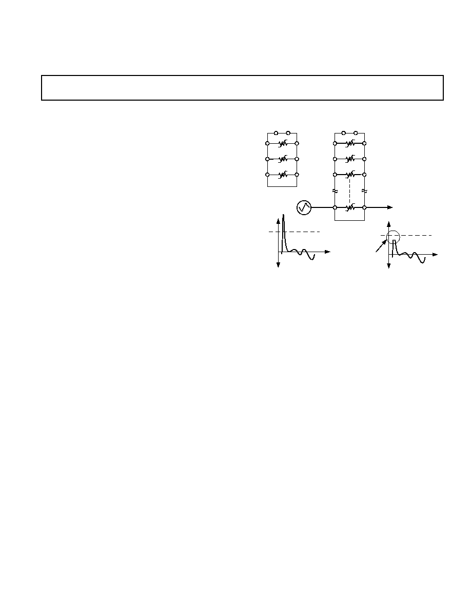
FUNCTIONAL BLOCK DIAGRAMS
ADG466
ADG467
V
D1
V
D2
V
D3
V
S1
V
S2
V
S3
V
D1
V
D2
V
D3
V
D8
V
S1
V
S2
V
S3
V
S8
V
DD
V
SS
V
DD
V
SS
V
IN
V
DD
V
DD
V
IN
V
OUT
OUTPUT CLAMPED
@ V
DD
1.5V
V
OUT
GENERAL DESCRIPTION
The ADG466 and ADG467 are triple and octal channel pro-
tectors, respectively. The channel protector is placed in series
with the signal path. The channel protector will protect sensitive
components from voltage transience in the signal path whether
the power supplies are present or not. Because the channel
protection works whether the supplies are present or not, the
channel protectors are ideal for use in applications where
correct power sequencing can't always be guaranteed (e.g., hot-
insertion rack systems) to protect analog inputs. This is dis-
cussed further, and some example circuits are given in the
Applications section of this data sheet.
Each channel protector has an independent operation and con-
sists of an n-channel MOSFET, a p-channel MOSFET and an
n-channel MOSFET, connected in series. The channel protec-
tor behaves just like a series resistor during normal operation,
i.e., (V
SS
+ 2 V) < V
IN
< (V
DD
1.5 V). When a channel's ana-
log input exceeds the power supplies (including V
DD
and V
SS
=
0 V), one of the MOSFETs will switch off, clamping the output
to either V
SS
+ 2 V or V
DD
1.5 V. Circuitry and signal source
protection is provided in the event of an overvoltage or power
loss. The channel protectors can withstand overvoltage inputs
from 40 V to +40 V. See the Circuit Information section of
this data sheet.
The ADG466 and ADG467 can operate off both bipolar and
unipolar supplies. The channels are normally on when power is
connected and open circuit when power is disconnected. With
power supplies of
±
15 V, the on-resistance of the ADG466 and
FEATURES
Fault and Overvoltage Protection up to 40 V
Signal Paths Open Circuit with Power Off
Signal Path Resistance of R
ON
with Power On
44 V Supply Maximum Ratings
Low On Resistance
ADG466/ADG467 60
typ
1 nA Max Path Current Leakage @ +25 C
Low R
ON
Match (5
max)
Low Power Dissipation 0.8
W typ
Latch-Up Proof Construction
APPLICATIONS
ATE Equipment
Sensitive Measurement Equipment
Hot-Insertion Rack Systems
ADG467 is 60
typ with a leakage current of
±
1 nA max.
When power is disconnected, the input leakage current is ap-
proximately
±
5 nA typ.
The ADG466 is available in 8-lead DIP, SOIC and
µ
SOIC
packages. The ADG467 is available in an 18-lead SOIC package
and a 20-lead SSOP package.
PRODUCT HIGHLIGHTS
1. Fault Protection.
The ADG466 and ADG467 can withstand continuous volt-
age inputs from 40 V to +40 V. When a fault occurs due to
the power supplies being turned off or due to an overvoltage
being applied to the ADG466 and ADG467, the output is
clamped. When power is turned off, current is limited to the
microampere level.
2. Low Power Dissipation.
3. Low R
ON
.
ADG466/ADG467 60
typ.
4. Trench Isolation Latch-Up Proof Construction.
A dielectric trench separates the p- and n-channel MOSFETs
thereby preventing latch-up.

2
REV. A
ADG466/ADG467SPECIFICATIONS
Dual Supply
1
ADG466
ADG467
Parameter
+25 C
B
1
+25 C
B
1
Units
Test Conditions/Comments
FAULT PROTECTED CHANNEL
Fault-Free Analog Signal Range
2
V
SS
+ 1.2
V
SS
+ 1.2
V min
Output Open Circuit
V
DD
0.8
V
DD
0.8
V max
R
ON
60
75
62
80
typ
10 V
V
S
+10 V, I
S
= 1 mA
80
95
max
R
ON
3
4
6
max
5 V
V
S
+5 V
R
ON
Match
4
6
5
6
max
V
S
=
±
10 V, I
S
= 1 mA
LEAKAGE CURRENTS
Channel Output Leakage, I
S(ON)
V
S
= V
D
=
±
10 V
(without Fault Condition)
±
0.1
±
1
±
0.04
±
0.2
nA typ
±
1
±
5
±
1
±
5
nA max
Channel Input Leakage, I
D(ON)
V
S
=
±
25 V
(with Fault Condition)
±
0.2
±
0.4
±
0.2
±
0.4
nA typ
V
D
= Open Circuit
±
2
±
5
±
2
±
5
nA max
Channel Input Leakage, I
D(OFF)
V
DD
= 0 V, V
SS
= 0 V
(with Power Off and Fault)
±
0.5
±
2
±
0.5
±
2
nA typ
V
S
=
±
35 V,
±
1
±
5
±
2
±
10
nA max
V
D
= Open Circuit
Channel Input Leakage, I
D(OFF)
V
DD
= 0 V, V
SS
= 0 V
(with Power Off and Output S/C)
±
0.005
±
0.1
±
0.006
±
0.16
µ
A typ
V
S
=
±
35 V, V
D
= 0 V
±
0.015
±
0.5
±
0.015
±
0.5
µ
A max
POWER REQUIREMENTS
I
DD
±
0.05
±
0.05
µ
A typ
±
0.5
±
8
±
0.5
±
8
µ
A max
I
SS
±
0.05
±
0.05
µ
A typ
±
0.5
±
8
±
0.5
±
8
µ
A max
V
DD
/V
SS
0
0
0
0
V min
±
20
±
20
±
20
±
20
V max
NOTES
1
Temperature range is as follows: B Version: 40
°
C to +85
°
C.
2
Guaranteed by design, not subject to production test.
Specifications subject to change without notice.
(V
DD
= +15 V, V
SS
= 15 V, GND = 0 V, unless otherwise noted)
ADG466/ADG467
3
REV. A
ABSOLUTE MAXIMUM RATINGS
1
(T
A
= +25
°
C unless otherwise noted)
V
DD
to V
SS
. . . . . . . . . . . . . . . . . . . . . . . . . . . . . . . . . . . . +44 V
V
S
, V
D
, Analog Input Overvoltage with Power ON
2
. . . . . . . . . . . . . . . . . . . . . . . . . . . . V
SS
20 V to V
DD
+ 20 V
V
S
, V
D
, Analog Input Overvoltage with Power OFF
2
. . . . . . . . . . . . . . . . . . . . . . . . . . . . . . . . . . . . 35 V to +35 V
Continuous Current, S or D . . . . . . . . . . . . . . . . . . . . . 20 mA
Peak Current, S or D . . . . . . . . . . . . . . . . . . . . . . . . . . . 40 mA
(Pulsed at 1 ms, 10% Duty Cycle Max)
Operating Temperature Range
Industrial (B Version) . . . . . . . . . . . . . . . . . 40
°
C to +85
°
C
Storage Temperature Range . . . . . . . . . . . . . 65
°
C to +125
°
C
Junction Temperature . . . . . . . . . . . . . . . . . . . . . . . . . +150
°
C
Plastic DIP Package
JA
, Thermal Impedance . . . . . . . . . . . . . . . . . . . . 125
°
C/W
Lead Temperature, Soldering (10 sec) . . . . . . . . . . . +260
°
C
SOIC Package
JA
, Thermal Impedance . . . . . . . . . . . . . . . . . . . . 160
°
C/W
Lead Temperature, Soldering
Vapor Phase (60 sec) . . . . . . . . . . . . . . . . . . . . . . +215
°
C
Infrared (15 sec) . . . . . . . . . . . . . . . . . . . . . . . . . . +220
°
C
µ
SOIC Package
JA
, Thermal Impedance . . . . . . . . . . . . . . . . . . . . 160
°
C/W
Lead Temperature, Soldering
Vapor Phase (60 sec) . . . . . . . . . . . . . . . . . . . . . . +215
°
C
Infrared (15 sec) . . . . . . . . . . . . . . . . . . . . . . . . . . +220
°
C
SSOP Package
JA
, Thermal Impedance . . . . . . . . . . . . . . . . . . . . 130
°
C/W
Lead Temperature, Soldering
Vapor Phase (60 sec) . . . . . . . . . . . . . . . . . . . . . . +215
°
C
Infrared (15 sec) . . . . . . . . . . . . . . . . . . . . . . . . . . +220
°
C
NOTES
1
Stresses above those listed under Absolute Maximum Ratings may cause perma-
nent damage to the device. This is a stress rating only; functional operation of the
device at these or any other conditions above those listed in the operational sections
of this specification is not implied. Exposure to absolute maximum rating condi-
tions for extended periods may affect device reliability. Only one absolute maxi-
mum rating may be applied at any one time.
2
Overvoltages at S or D will be clamped by the channel protector, see Circuit
Information section of the data sheet.
CAUTION
ESD (electrostatic discharge) sensitive device. Electrostatic charges as high as 4000 V readily
accumulate on the human body and test equipment and can discharge without detection.
Although the ADG466/ADG467 features proprietary ESD protection circuitry, permanent
damage may occur on devices subjected to high energy electrostatic discharges. Therefore, proper
ESD precautions are recommended to avoid performance degradation or loss of functionality.
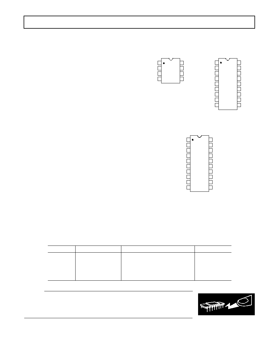
PIN CONFIGURATIONS
8-Lead
DIP, SOIC
18-Lead
and SOIC
SOIC
1
2
3
4
8
7
6
5
TOP VIEW
(Not to Scale)
ADG466
V
D1
V
S3
V
S2
V
S1
V
DD
V
D2
V
D3
V
SS
14
13
12
11
17
16
15
18
10
9
8
1
2
3
4
7
6
5
TOP VIEW
(Not to Scale)
ADG467
V
D1
V
S3
V
S2
V
S1
V
DD
V
D2
V
D3
V
D4
V
S6
V
S5
V
S4
V
D5
V
D6
V
D7
V
D8
V
SS
V
S8
V
S7
20-Lead
SSOP
V
D1
V
S3
V
S2
V
S1
V
DD
V
D2
V
D3
V
D4
V
S6
V
S5
V
S4
V
D5
V
D6
V
D7
V
D8
V
SS
V
S8
V
S7
14
13
12
11
17
16
15
20
19
18
10
9
8
1
2
3
4
7
6
5
TOP VIEW
(Not to Scale)
ADG467
NC = NO CONNECT
NC
NC
ORDERING GUIDE
Model
Temperature Range
Package Description
Package Options
ADG466BN
40
°
C to +85
°
C
8-Lead Plastic DIP
N-8
ADG466BR
40
°
C to +85
°
C
8-Lead Small Outline Package
SO-8
ADG466BRM
40
°
C to +85
°
C
8-Lead Micro Small Outline Package
RM-8
ADG467BR
40
°
C to +85
°
C
18-Lead Small Outline Package
R-18
ADG467BRS
40
°
C to +85
°
C
20-Lead Shrink Small Outline Package
RS-20
WARNING!
ESD SENSITIVE DEVICE
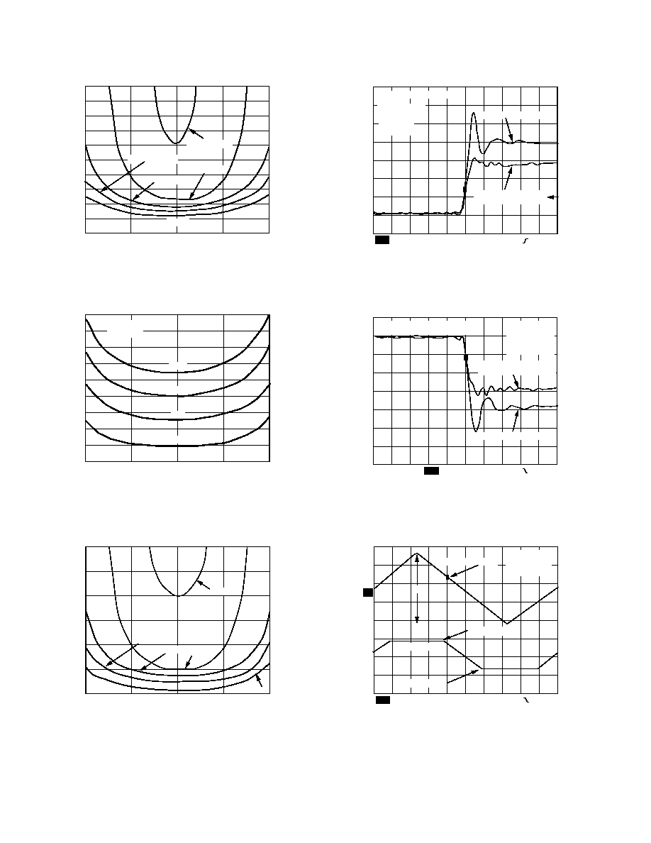
ADG466/ADG467Typical Performance Characteristics
4
REV. A
ADG466
V
D
Volts
R
ON
80
75
30
10
10
5
0
5
60
45
40
35
70
65
50
55
V
DD
, V
SS
= 5V
V
DD
, V
SS
= 10V
16.5V
V
DD
, V
SS
= 13.5V
V
DD
, V
SS
= 15V
Figure 1. On Resistance as a Function of V
DD
and V
D
(Input Voltage)
70
65
25
10
10
5
0
5
50
40
35
30
60
55
45
125 C
85 C
25 C
40 C
V
D
Volts
R
ON
V
DD
= +15V
V
SS
= 15V
Figure 2. On Resistance as a Function of Temperature
and V
D
(Input Voltage)
16.5V
ADG467
V
D
Volts
105
95
45
10
10
5
R
ON
0
5
85
75
65
55
5V
15V
13.5V
10V
Figure 3. On Resistance as a Function of V
DD
and V
D
(Input Voltage)
Ch1
10V
500mV
5.00V
Ch2
5.00V
M50.0ns
Ch1
0V
5V
15V
5V
5V TO +15V STEP INPUT
CHANNEL PROTECTOR
OUTPUT
POSITIVE OVERVOLTAGE
R
LOAD
= 100k
ON INPUT
C
LOAD
= 100pF
V
DD
= +10V
V
SS
= 10V
Figure 4. Positive Overvoltage Transience Response
Ch2
500mV
Ch1
5.00V
5.00V
M50.0ns
Ch1
NEGATIVE OVERVOLTAGE
ON INPUT
R
LOAD
= 100k
C
LOAD
= 100pF
V
DD
= +10V
V
SS
= 10V
CHANNEL PROTECTOR
OUTPUT
5V TO 15V STEP INPUT
10V
5V
0V
5V
15V
Figure 5. Negative Overvoltage Transience Response
1
500mV
5.00V
Ch2
5.00V
M100 s
Ch1
2
OUTPUT
V
CLAMP
=4V
V
CLAMP
=4.5V
10V TO +10 V INPUT
R
LOAD
=100k
V
DD
=+5V
V
SS
=5V
Ch1
20V
Figure 6. Overvoltage Ramp
ADG466/ADG467
5
REV. A
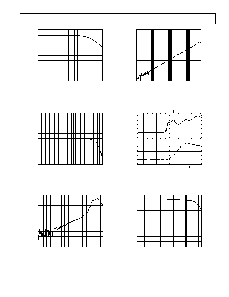
1M
10M
FREQUENCY Hz
30M
10
12
14
16
18
20
22
24
26
28
30
GAIN dB
Figure 7. Frequency Response (Magnitude) of the ADG467,
V
DD
/V
SS
=
±
15 V and Input Signal Level of
±
100 mV
100
10M
1k
10k
100k
1M
FREQUENCY Hz
105.359
82.859
60.359
37.859
15.359
7.141
29.641
52.161
76.641
97.161
PHASE Degrees
Figure 8. Frequency Response (Phase) of the ADG467,
V
DD
/V
SS
=
±
15 V and Input Signal Level of
±
100 mV
100k
10k
FREQUENCY Hz
1M
10M
40M
10
20
30
40
50
60
70
80
90
100
110
CROSSTALK dB
Figure 9. Crosstalk Between Adjacent Channels of the
ADG467, V
DD
/V
SS
=
±
15 V and Input Signal Level of
±
100 mV
10k
40M
100k
1M
10M
FREQUENCY Hz
0
10
20
30
40
50
60
70
80
90
100
OFF ISOLATION dB
Figure 10. Off Isolation of the ADG467, V
DD
/V
SS
= 0 V and
Input Signal Level of
±
100 mV
CH1
2.2V
2.00V
CH2
2.00V
M 10.0ns
CH1
2
1
TEK RUN: 5.00GS/s ET SAMPLE
12.2ns
11.8ns
Figure 11. Propagation Delay Through ADG467, V
DD
/V
SS
=
±
15 V, Channel 1 Input and Channel 2 Output
100k
40M
1M
10M
FREQUENCY Hz
10
14
18
22
26
30
36
38
42
46
50
GAIN dB
Figure 12. Frequency Response (Magnitude) of the ADG466,
V
DD
/V
SS
=
±
15 V and Input Signal Level of
±
100 mV
ADG466/ADG467
6
REV. A
100
10M
1k
10k
100k
1M
FREQUENCY Hz
40M
105.3
82.8
60.3
37.8
15.3
7.1
29.6
52.1
76.6
92.1
PHASE Degrees
Figure 13. Frequency Response (Phase) of the ADG466, V
DD
/
V
SS
=
±
15 V and Input Signal Level of
±
100 mV
10k
40M
100k
1M
10M
FREQUENCY Hz
0
10
20
30
40
50
60
70
80
90
100
CROSSTALK dB
Figure 14. Crosstalk Between Adjacent Channels of the
ADG466, V
DD
/V
SS
=
±
15 V and Input Signal Level of
±
100 mV
10k
40M
100k
1M
10M
FREQUENCY Hz
0
10
20
30
40
50
60
70
80
90
100
OFF ISOLATION dB
Figure 15. Off Isolation of the ADG466, V
DD
/V
SS
= 0 V and
Input Signal Level of
±
100 mV
CH1
760V
1.00V
CH2
1.00V
M 20.0ns
CH1
2
1
TEK RUN: 2.5GS/s ET SAMPLE
18.0ns
22.0ns
Figure 16. Propagation Delay Through ADG466, V
DD
/V
SS
=
±
15 V, Channel 1 Input and Channel 2 Output
ADG466/ADG467
7
REV. A
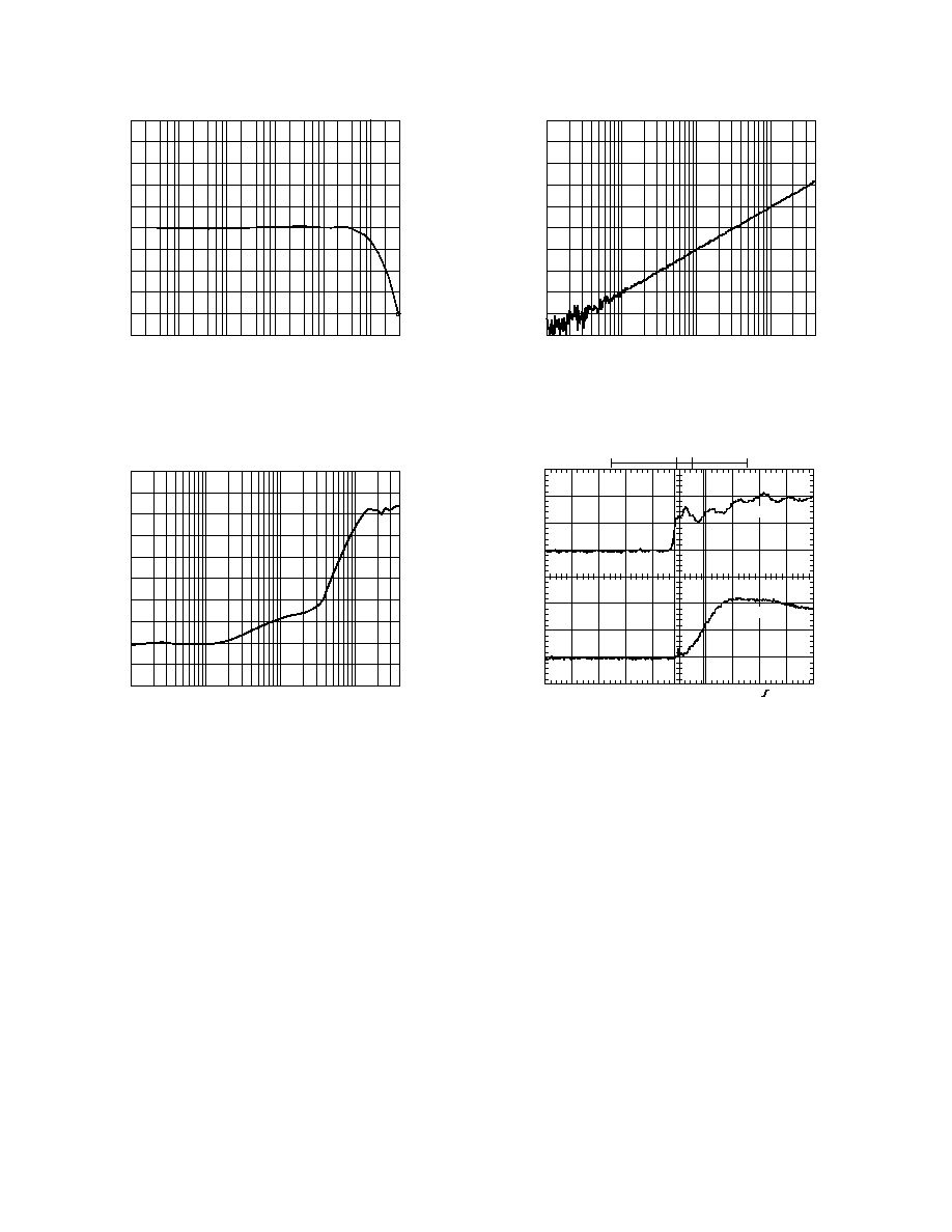
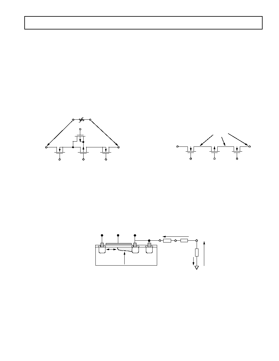
CIRCUIT INFORMATION
Figure 17 below shows a simplified schematic of a channel
protector circuit. The circuit is made up of four MOS transis-
tors--two NMOS and two PMOS. One of the PMOS devices
does not lie directly in the signal path but is used to connect the
source of the second PMOS device to its backgate. This has the
effect of lowering the threshold voltage and so increasing the
input signal range of the channel for normal operation. The
source and backgate of the NMOS devices are connected for the
same reason. During normal operation the channel protectors
have a resistance of 60
typ. The channel protectors are very
low power devices, and even under fault conditions the supply
current is limited to sub microampere levels. All transistors are
dielectrically isolated from each other using a trench isolation
method. This makes it impossible to latch up the channel
protectors. For an explanation, see Trench Isolation section.
NMOS
PMOS
PMOS
NMOS
V
DD
V
SS
V
SS
V
DD
Figure 17. The Channel Protector Circuit
Overvoltage Protection
When a fault condition occurs on the input of a channel protec-
tor, the voltage on the input has exceeded some threshold volt-
age set by the supply rail voltages. The threshold voltages are
related to the supply rails as follows. For a positive overvoltage,
the threshold voltage is given by V
DD
V
T
where V
TN
is the
threshold voltage of the NMOS transistor (1.5 V typ). In the
case of a negative overvoltage the threshold voltage is given by
V
SS
V
TP
where V
TP
is the threshold voltage of the PMOS de-
vice (2 V typ). If the input voltage exceeds these threshold volt-
ages, the output of the channel protector (no load) is clamped at
these threshold voltages. However, the channel protector output
will clamp at a voltage that is inside these thresholds if the out-
put is loaded. For example with an output load of 1 k
, V
DD
=
15 V and a positive overvoltage. The output will clamp at V
DD
V
TN
V = 15 V 1.5 V 0.6 V = 12.9 V where
V is due to I
×
R voltage drop across the channels of the MOS devices (see
Figure 19). As can be seen from Figure 19, the current during
fault condition is determined by the load on the output (i.e.,
V
CLAMP
/R
L
). However, if the supplies are off, the fault current is
limited to the nano-ampere level.
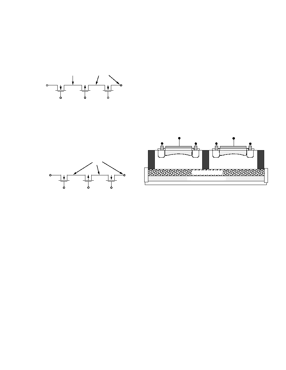
Figures 18, 20 and 21 show the operating conditions of the
signal path transistors during various fault conditions. Figure 18
shows how the channel protectors operate when a positive over-
voltage is applied to the channel protector.
NMOS
PMOS
NMOS
V
DD
(+15V)
V
SS
(15V)
V
DD
(+15V)
POSITIVE
OVERVOLTAGE
(+20V)
V
DD
V
TN
*
(+13.5V)
*V
TN
= NMOS THRESHOLD VOLTAGE (+1.5V)
NON-
SATURATED
NON-
SATURATED
SATURATED
Figure 18. Positive Overvoltage on the Channel Protector
The first NMOS transistor goes into a saturated mode of opera-
tion as the voltage on its Drain exceeds the Gate voltage (V
DD
)
the threshold voltage (V
TN
). This situation is shown in Figure
19. The potential at the source of the NMOS device is equal to
V
DD
V
TN
. The other MOS devices are in a nonsaturated mode of
operations.
V
S
N +
(V
DD
=15V)
V
D
P
N +
N +
(+20V)
(+13.5V)
OVERVOLTAGE
OPERATION
(SATURATED)
V
T
= 1.5V
(V
G
V
T
= 13.5V)
V
G
EFFECTIVE
SPACE CHARGE
REGION
N CHANNEL
NMOS
PMOS
NONSATURATED
OPERATION
R
L
V
I
OUT
V
CLAMP
Figure 19. Positive Overvoltages Operation of the Channel Protector
ADG466/ADG467
8
REV. A
When a negative overvoltage is applied to the channel protector
circuit, the PMOS transistor enters a saturated mode of opera-
tion as the drain voltage exceeds V
SS
V
TP
. See Figure 20 be-
low. As in the case of the positive overvoltage, the other MOS
devices are nonsaturated.
NMOS
PMOS
NMOS
V
DD
(+15V)
V
SS
(15V)
V
DD
(+15V)
NEGATIVE
OVERVOLTAGE
(20V)
V
SS
V
TP
*
(13V)
*V
TP
= PMOS THRESHOLD VOLTAGE (2V)
NEGATIVE
OVERVOLTAGE
(20V)
NON-
SATURATED
NON-
SATURATED
SATURATED
Figure 20. Negative Overvoltage on the Channel Protector
The channel protector is also functional when the supply rails
are down (e.g., power failure) or momentarily unconnected
(e.g., rack system). This is where the channel protector has an
advantage over more conventional protection methods such as
diode clamping (see Applications Information). When V
DD
and
V
SS
equal 0 V, all transistors are off and the current is limited to
subnano-ampere levels (see Figure 21).
NMOS
PMOS
NMOS
V
DD
(0V)
V
SS
(0V)
V
DD
(0V)
POSITIVE OR
NEGATIVE
OVERVOLTAGE
(0V)
OFF
OFF
OFF
Figure 21. Channel Protector Supplies Equal to Zero Volts
TRENCH ISOLATION
The MOS devices that make up the channel protector are iso-
lated from each other by an oxide layer (trench) (see Figure 22).
When the NMOS and PMOS devices are not electrically iso-
lated from each other, there exists the possibility of "latch-up"
caused by parasitic junctions between CMOS transistors. Latch-
up is caused when P-N junctions that are normally reverse bi-
ased become forward biased, causing large currents to flow,
which can be destructive.
CMOS devices are normally isolated from each other by Junc-
tion Isolation. In Junction Isolation, the N and P wells of the
CMOS transistors form a diode that is reverse-biased under
normal operation. However, during overvoltage conditions, this
diode becomes forward biased. A Silicon-Controlled Rectifier
(SCR) type circuit is formed by the two transistors causing a
significant amplification of the current that, in turn, leads to
latch-up. With Trench Isolation, this diode is removed; the
result is a latch-up proof circuit.
V
G
V
D
P-CHANNEL
P+
P+
V
S
N
V
G
V
D
N-CHANNEL
N+
N+
V
S
P
T
R
E
N
C
H
T
R
E
N
C
H
T
R
E
N
C
H
BURIED OXIDE LAYER
SUBSTRATE (BACKGATE)
Figure 22. Trench Isolation
ADG466/ADG467
9
REV. A
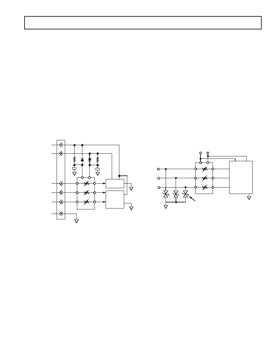
APPLICATIONS INFORMATION
Overvoltage and Power Supply Sequencing Protection
The ADG466 and ADG467 are ideal for use in applications
where input overvoltage protection is required and correct
power supply sequencing cannot always be guaranteed. The
overvoltage protection ensures that the output voltage of the
channel protector will not exceed the threshold voltages set by
the supplies (see Circuit Information) when there is an overvolt-
age on the input. When the input voltage does not exceed these
threshold voltages, the channel protector behaves like a series
resistor (60
typ). The resistance of the channel protector does
vary slightly with operating conditions (see Typical Performance
Graphs).
The power sequencing protection is afforded by the fact that
when the supplies to the channel protector are not connected,
the channel protector becomes a high resistance device. Under
this condition all transistors in the channel protector are off and
the only currents that flow are leakage currents, which are at the
µ
A level.
V
DD
V
SS
+5V
5V
EDGE
CONNECTOR
ADG466
ADC
CONTROL
LOGIC
ANALOG IN
2.5V TO +2.5V
LOGIC
LOGIC
GND
Figure 23. Overvoltage and Power Supply Sequencing
Protection
Figure 23 shows a typical application that requires overvoltage
and power supply sequencing protection. The application shows
a Hot-Insertion rack system. This involves plugging a circuit
board or module into a live rack via an edge connector. In this
type of application it is not possible to guarantee correct power
supply sequencing. Correct power supply sequencing means
that the power supplies should be connected before any external
signals. Incorrect power sequencing can cause a CMOS device
to "latch up." This is true of most CMOS devices regardless of
the functionality. RC networks are used on the supplies of the
channel protector (Figure 23) to ensure that the rest of the
circuitry is powered up before the channel protectors. In this
way, the outputs of the channel protectors are clamped well
below V
DD
and V
SS
until the capacitors are charged. The diodes
ensure that the supplies on the channel protector never exceed
the supply rails of the board when it is being disconnected.
Again this ensures that signals on the inputs of the CMOS de-
vices never exceed the supplies.
High Voltage Surge Suppression
The ADG466 and ADG467 are not intended for use in high
voltage applications like surge suppression. The ADG466
and ADG467 have breakdown voltages of V
SS
20 V and
V
DD
+ 20 V on the inputs when the power supplies are con-
nected. When the power supplies are disconnected, the break-
down voltages on the input of the channel protector are
±
35 V.
In applications where inputs are likely to be subject to overvolt-
ages exceeding the breakdown voltages quoted for the channel
protectors, transient voltage suppressors (TVSs) should be used.
These devices are commonly used to protect vulnerable circuits
from electric overstress such as that caused by electrostatic
discharge, inductive load switching and induced lightning. How-
ever, TVSs can have a substantial standby (leakage) current
(300
µ
A typ) at the reverse standoff voltage. The reverse standoff
voltage of a TVS is the normal peak operating voltage of the
circuit. Also TVS offer no protection against latch-up of sensitive
CMOS devices when the power supplies are off. The best solution
is to use a channel protector in conjunction with a TVS to provide
the best leakage current specification and circuit protection.
ADG466
V
DD
= +5V
V
SS
= 5V
ADC
TVSs
BREAKDOWN
VOLTAGE = 20V
Figure 24. High Voltage Protection
Figure 24 shows an input protection scheme that uses both a
TVS and channel protector. The TVS is selected with a reverse
standoff voltage that is much greater than operating voltage of
the circuit (TVSs with higher breakdown voltages tend to have
better standby leakage current specifications) but is inside the
breakdown voltage of the channel protector. This circuit pro-
tects the circuitry whether the power supplies are present
or not.
ADG466/ADG467
10
REV. A
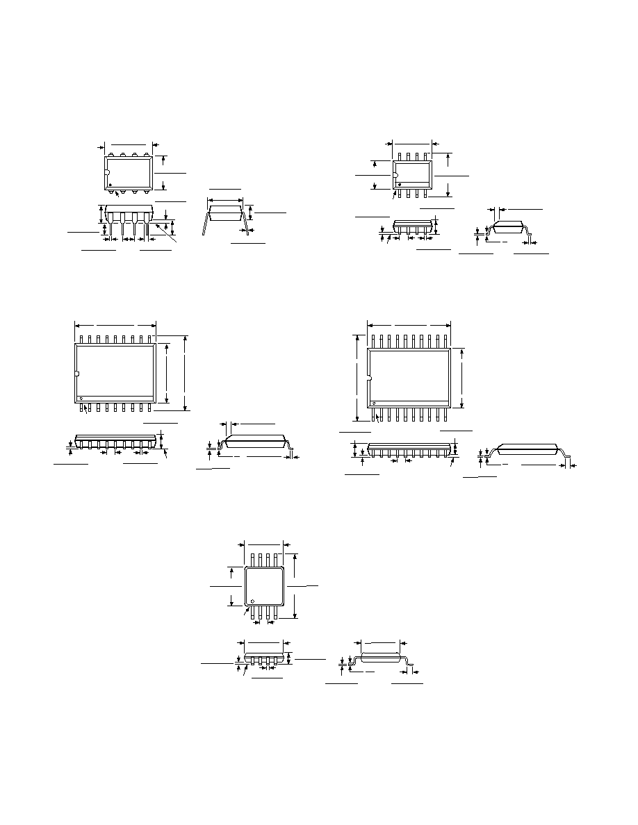
8-Lead Plastic DIP (N-8)
8
1
4
5
0.430 (10.92)
0.348 (8.84)
0.280 (7.11)
0.240 (6.10)
PIN 1
SEATING
PLANE
0.022 (0.558)
0.014 (0.356)
0.060 (1.52)
0.015 (0.38)
0.210 (5.33)
MAX
0.130
(3.30)
MIN
0.070 (1.77)
0.045 (1.15)
0.100
(2.54)
BSC
0.160 (4.06)
0.115 (2.93)
0.325 (8.25)
0.300 (7.62)
0.015 (0.381)
0.008 (0.204)
0.195 (4.95)
0.115 (2.93)
18-Lead Small Outline IC (R-18)
SEATING
PLANE
0.0118 (0.30)
0.0040 (0.10)
0.0192 (0.49)
0.0138 (0.35)
0.1043 (2.65)
0.0926 (2.35)
0.0500
(1.27)
BSC
0.0125 (0.32)
0.0091 (0.23)
0.0500 (1.27)
0.0157 (0.40)
8
°
0
°
0.0291 (0.74)
0.0098 (0.25)
x 45
°
18
10
9
1
0.4625 (11.75)
0.4469 (11.35)
0.4193 (10.65)
0.3937 (10.00)
0.2992 (7.60)
0.2914 (7.40)
PIN 1
8-Lead Small Outline IC (SO-8)
0.1968 (5.00)
0.1890 (4.80)
8
5
4
1
0.2440 (6.20)
0.2284 (5.80)
PIN 1
0.1574 (4.00)
0.1497 (3.80)
0.0688 (1.75)
0.0532 (1.35)
SEATING
PLANE
0.0098 (0.25)
0.0040 (0.10)
0.0192 (0.49)
0.0138 (0.35)
0.0500
(1.27)
BSC
0.0098 (0.25)
0.0075 (0.19)
0.0500 (1.27)
0.0160 (0.41)
8
°
0
°
0.0196 (0.50)
0.0099 (0.25)
x 45
°
20-Lead Shrink Small Outline Package (RS-20)
20
11
10
1
0.295 (7.50)
0.271 (6.90)
0.311 (7.9)
0.301 (7.64)
0.212 (5.38)
0.205 (5.21)
PIN 1
SEATING
PLANE
0.008 (0.203)
0.002 (0.050)
0.07 (1.78)
0.066 (1.67)
0.0256
(0.65)
BSC
0.078 (1.98)
0.068 (1.73)
0.009 (0.229)
0.005 (0.127)
0.037 (0.94)
0.022 (0.559)
8
°
0
°
8-Lead Micro Small Outline IC (RM-8)
8
5
4
1
0.122 (3.10)
0.114 (2.90)
0.199 (5.05)
0.187 (4.75)
PIN 1
0.0256 (0.65) BSC
0.122 (3.10)
0.114 (2.90)
SEATING
PLANE
0.006 (0.15)
0.002 (0.05)
0.018 (0.46)
0.008 (0.20)
0.043 (1.09)
0.037 (0.94)
0.120 (3.05)
0.112 (2.84)
0.011 (0.28)
0.003 (0.08)
0.028 (0.71)
0.016 (0.41)
33
°
27
°
0.120 (3.05)
0.112 (2.84)
OUTLINE DIMENSIONS
Dimensions shown in inches and (mm).
C2207a05/98
PRINTED IN U.S.A.