 | ÐлекÑÑоннÑй компоненÑ: ADG612 | СкаÑаÑÑ:  PDF PDF  ZIP ZIP |
Äîêóìåíòàöèÿ è îïèñàíèÿ www.docs.chipfind.ru
REV. A
Information furnished by Analog Devices is believed to be accurate and
reliable. However, no responsibility is assumed by Analog Devices for its
use, nor for any infringements of patents or other rights of third parties
that may result from its use. No license is granted by implication or
otherwise under any patent or patent rights of Analog Devices.
a
AD8565/AD8566/AD8567
One Technology Way, P.O. Box 9106, Norwood, MA 02062-9106, U.S.A.
Tel: 781/329-4700
www.analog.com
Fax: 781/326-8703
© Analog Devices, Inc., 2001
16 V Rail-to-Rail
Operational Amplifiers
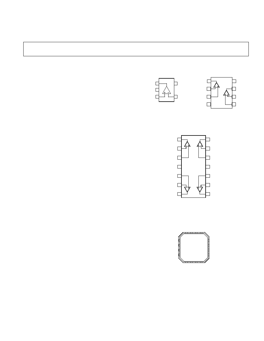
PIN CONFIGURATIONS
FEATURES
Single-Supply Operation: 4.5 V to 16 V
Input Capability Beyond the Rails
Rail-to-Rail Output Swing
Continuous Output Current: 35 mA
Peak Output Current: 250 mA
Offset Voltage: 10 mV
Slew Rate: 6 V/ s
Unity Gain Stable with Large Capacitive Loads
Supply Current: 700 A per Amplifier
APPLICATIONS
LCD Reference Drivers
Portable Electronics
Communications Equipment
GENERAL DESCRIPTION
The AD8565, AD8566, and AD8567 are low-cost single supply
rail-to-rail input and output operational amplifiers optimized for
LCD monitor applications. They are built on an advanced high-
voltage CBCMOS process. The AD8565 contains a single
amplifier, the AD8566 has two amplifiers, and the AD8567 has
four amplifiers.
These LCD op amps have high slew rates, 35 mA continuous
output drive, 250 mA peak output drive, and high capacitive load
drive capability. They have wide supply range and offset voltages
below 10 mV. The AD8565, AD8566, and AD8567 are ideal for
LCD grayscale reference buffer and V
COM
applications.
The AD8565, AD8566, and AD8567 are specified over the 40
°C
to +85
°C temperature range. The AD8565 single is available in a
5-lead SC70 package. The AD8566 dual is available in an 8-lead
MSOP package. The AD8567 quad is available in a 14-lead
TSSOP package and a 16-lead lead frame Chip Scale Package.
5-Lead SC70
(KS Suffix)
1
2
3
5
4 IN
+IN
V
OUT
AD8565
V+
14-Lead TSSOP
(RU Suffix)
OUT B
+IN B
IN B
V+
IN A
+IN A
OUT A
7
8
5
10
6
9
4
11
2
13
3
12
1
14
OUT C
+IN C
IN C
V
IN D
+IN D
OUT D
AD8567
16-Lead CSP
(CP Suffix)
TOP VIEW
16
5
13
8
9
12
1
4
14
15
2
3
7
6
11
10
IN D
+IN D
V
+IN C
IN A
+IN A
V+
+IN B
NC
OUT A
OUT D
NC
IN B
OUT B
OUT C
IN C
AD8567
NC = NO CONNECT
8-Lead MSOP
(RM Suffix)
4
5
2
7
3
6
1
8
OUT A
IN A
+IN A
V
V+
OUT B
IN B
+IN B
AD8566

2
REV. A
AD8565/AD8566/AD8567SPECIFICATIONS
Electrical Characteristics
Parameter
Symbol
Conditions
Min
Typ
Max
Unit
INPUT CHARACTERISTICS
Offset Voltage
V
OS
2
10
mV
Offset Voltage Drift
V
OS
/
T
40
°C T
A
+85°C
5
µV/°C
Input Bias Current
I
B
80
600
nA
40
°C T
A
+85°C
800
nA
Input Offset Current
I
OS
1
80
nA
40
°C T
A
+85°C
130
nA
Input Voltage Range
Common-Mode Input
0.5
V
S
+ 0.5
V
Common-Mode Rejection Ratio
CMRR
V
CM
= 0 to V
S
,
40
°C T
A
+85°C
54
95
dB
Large Signal Voltage Gain
AVO
R
L
= 10 k
,
V
O
= 0.5 to (V
S
0.5 V)
3
10
V/mV
Input Impedance
Z
IN
400
k
Input Capacitance
C
IN
1
pF
OUTPUT CHARACTERISTICS
Output Voltage High
V
OH
I
L
= 100
µA
V
S
0.005
V
V
S
= 16 V, I
L
= 5 mA
15.85
15.95
V
40
°C T
A
+85°C
15.75
V
V
S
= 4.5 V, I
L
= 5 mA
4.2
4.38
V
40
°C T
A
+85°C
4.1
V
Output Voltage Low
V
OL
I
L
= 100
µA
5
mV
V
S
= 16 V, I
L
= 5 mA
42
150
mV
40
°C T
A
+85°C
250
mV
V
S
= 4.5 V, I
L
= 5 mA
95
300
mV
40
°C T
A
+85°C
400
mV
Continuous Output Current
I
OUT
35
mA
Peak Output Current
I
PK
V
S
= 16 V
250
mA
POWER SUPPLY
Supply Voltage
V
S
4.5
16
V
Power Supply Rejection Ratio
PSRR
V
S
= 4 V to 17 V,
40
°C T
A
+85°C
70
90
dB
Supply Current/Amplifier
I
SY
V
O
= V
S
/2, No Load
700
850
µA
40
°C T
A
+85°C
1
mA
DYNAMIC PERFORMANCE
Slew Rate
SR
R
L
= 10 k
, C
L
= 200 pF
4
6
V/
µs
Gain Bandwidth Product
GBP
R
L
= 10 k
, C
L
= 10 pF
5
MHz
3 dB Bandwidth
BW
R
L
= 10 k
, C
L
= 10 pF
6
MHz
Phase Margin
Øo
R
L
= 10 k
, C
L
= 10 pF
65
Degrees
Channel Separation
75
dB
NOISE PERFORMANCE
Voltage Noise Density
e
n
f = 1 kHz
2 6
nV/
Hz
e
n
f = 10 kHz
2 5
nV/
Hz
Current Noise Density
i
n
f = 10 kHz
0.8
pA/
Hz
Specifications subject to change without notice.
(4.5 V
V
S
16 V, V
CM
= V
S
/2, T
A
= 25 C, unless otherwise noted.)
AD8565/AD8566/AD8567
3
REV. A
ABSOLUTE MAXIMUM RATINGS
*
Supply Voltage (V
S
) . . . . . . . . . . . . . . . . . . . . . . . . . . . . . 18 V
Input Voltage . . . . . . . . . . . . . . . . . . . . . 0.5 V to V
S
+ 0.5 V
Differential Input Voltage . . . . . . . . . . . . . . . . . . . . . . . . . . V
S
Storage Temperature Range . . . . . . . . . . . . 65
°C to +150°C
Operating Temperature Range . . . . . . . . . . . 40
°C to +85°C
Junction Temperature Range . . . . . . . . . . . . 65
°C to +150°C
Lead Temperature Range (Soldering, 60 sec) . . . . . . . . 300
°C
*Stresses above those listed under Absolute Maximum Ratings may cause perma-
nent damage to the device. This is a stress rating only; functional operation of the
device at these or any other conditions above those listed in the operational
sections of this specification is not implied. Exposure to absolute maximum rating
conditions for extended periods may affect device reliability.
CAUTION
ESD (electrostatic discharge) sensitive device. Electrostatic charges as high as 4000 V readily
accumulate on the human body and test equipment and can discharge without detection. Although
the AD8565/AD8566/AD8567 features proprietary ESD protection circuitry, permanent damage
may occur on devices subjected to high-energy electrostatic discharges. Therefore, proper ESD
precautions are recommended to avoid performance degradation or loss of functionality.
WARNING!
ESD SENSITIVE DEVICE
ORDERING GUIDE
Temperature
Package
Branding
Model
*
Range
Package Description
Option
Information
AD8565AKS
40
°C to +85°C
5-Lead Plastic Surface-Mount
KS-5
ASA
AD8566ARM
40
°C to +85°C
8-Lead MINI_SOIC
RM-8
ATA
AD8567ARU
40
°C to +85°C
14-Lead Thin Shrink SO
RU-14
AD8567ACP
40
°C to +85°C
16-Terminal Leadless Frame Chip Scale
CP-16
*
Available in reels only.
Package Type
JA
1
JC
Unit
5-Lead SC70 (KS)
376
126
°C/W
8-Lead MSOP (RM)
210
45
°C/W
14-Lead TSSOP (RU)
180
35
°C/W
16-Lead LFCSP (CP)
38
2
30
2
°C/W
NOTES
1
JA
is specified for worst-case conditions, i.e.,
JA
is specified for device soldered
onto a circuit board for surface mount packages.
2
DAP is soldered down to PCB.
AD8565/AD8566/AD8567
4
REV. A
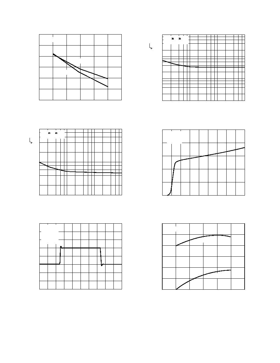
Typical Performance Characteristics
TEMPERATURE C
0
0.25
1.50
40
INPUT OFFSET VOLTAGE
mV
25
85
0.50
0.75
1.00
1.25
V
CM
= V
S
/2
V
S
= 16V
V
S
= 4.5V
TPC 1. Input Offset Voltage vs. Temperature
FREQUENCY Hz
10
1
0.1
10
10k
100
1k
4.5V V
S
16V
T
A
= 25 C
CURRENT NOISE DENSITY
pA Hz
TPC 2. Current Noise Density vs. Frequency
FREQUENCY 1 s/DIV
TIME
50mV/DIV
V
S
= 16V
R
L
= 10k
C
L
= 100pF
A
V
= +1
T
A
= 25 C
TPC 3. Small Signal Transient Response
VOLTAGE NOISE DENSITY
nV Hz
FREQUENCY Hz
1000
100
1
10
10k
100
1k
4.5V V
S
16V
T
A
= 25 C
10
TPC 4. Voltage Noise Density vs. Frequency
SUPPLY VOLTAGE V
1.0
0.8
0
0
18
2
SUPPLY CURRENT/AMPLIFIER
mA
4
6
8
10
12
14
16
0.6
0.4
0.2
V
O
= V
S
/2
A
V
= +1
T
A
= 25 C
TPC 5. Supply Current/Amplifier vs. Supply Voltage
TEMPERATURE C
0.80
0.75
0.50
40
SUPPLY CURRENT/AMPLIFIER
mA
25
85
0.70
0.65
0.60
0.55
V
CM
= V
S
/2
V
S
= 16V
V
S
= 4.5V
TPC 6. Supply Current/Amplifier vs. Temperature
AD8565/AD8566/AD8567
5
REV. A
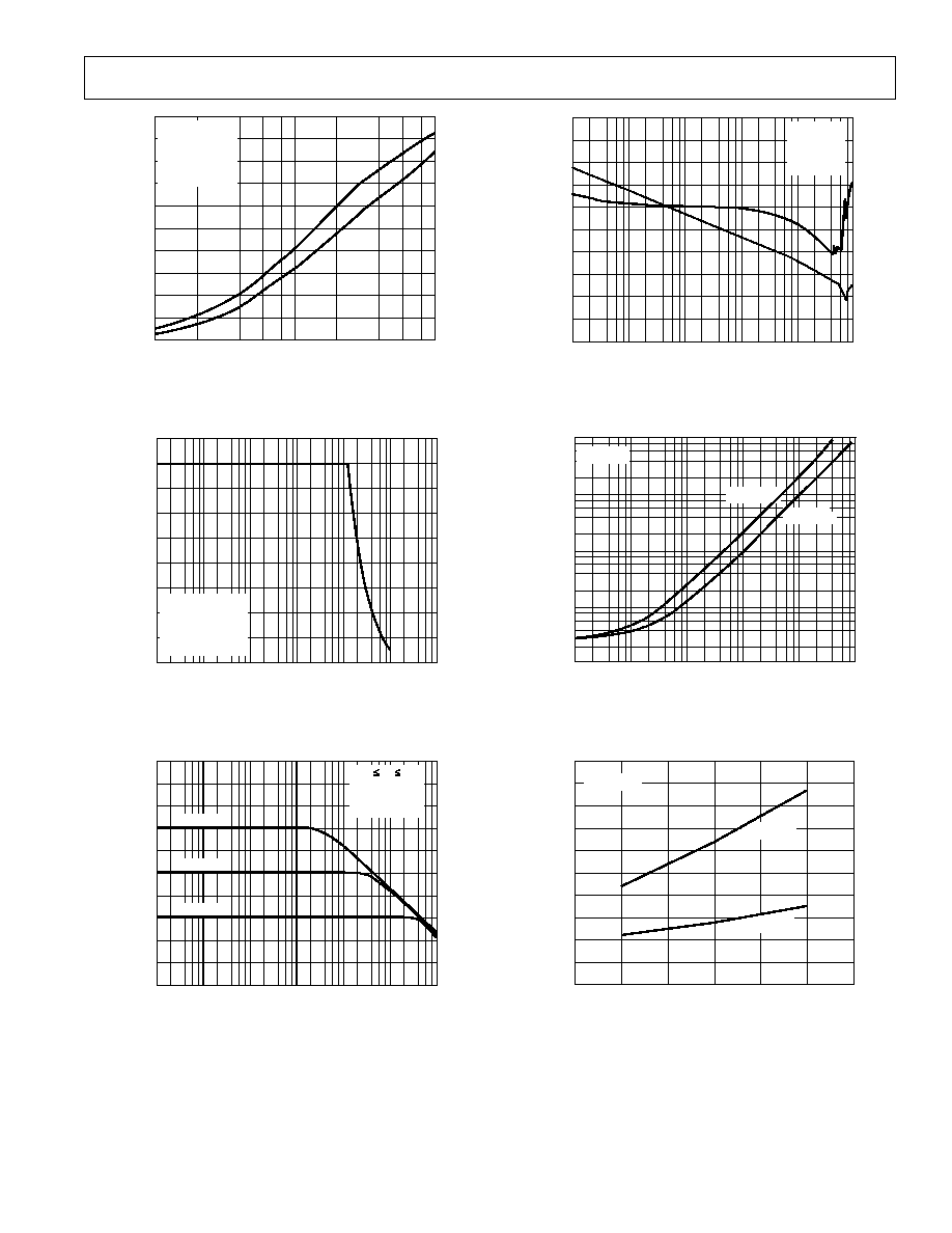
LOAD CAPACITANCE pF
100
90
0
10
1k
100
OVERSHOOT
%
80
70
60
50
40
30
20
10
V
S
= 16V
V
IN
= 100mV p-p
R
L
= 10k
A
V
= +1
T
A
= 25 C
OS
+OS
TPC 7. Small Signal Overshoot vs. Load Capacitance
FREQUENCY Hz
OUTPUT SWING
V
p-p
0
100
10
1k
10k
100k
1M
10M
2
4
6
8
10
12
14
16
18
V
S
= 16V
A
V
= +1
R
L
= 10k
DISTORTION < 1%
T
A
= 25 C
TPC 8. Closed-Loop Output Swing vs. Frequency
FREQUENCY Hz
CLOSED-LOOP GAIN
dB
100
10
1k
10k
100k
1M
10M
10
20
30
40
50
4.5V V
S
16V
R
L
= 10k
C
L
= 40pF
T
A
= 25 C
60
0
A
VCL
= 100
A
VCL
= 10
A
VCL
= +1
TPC 9. Closed-Loop Gain vs. Frequency
1k
100M
10k
GAIN
dB
100k
1M
10M
100
80
60
40
20
FREQUENCY Hz
45
90
135
180
0
225
270
PHASE SHIFT
C
V
S
= 16V
R
L
= 10k
C
L
= 40pF
T
A
= 25 C
0
TPC 10. Open-Loop Gain and Phase Shift vs. Frequency
LOAD CURRENT mA
10
0.1
0.001
100
0.01
0.1
1
10
1
100
V
S
= 4.5V
1k
T
A
= 25 C
V
S
= 16V
OUTPUT VOLTAGE
mV
TPC 11. Output Voltage to Supply Rail vs. Load Current
TEMPERATURE C
150
40
OUTPUT VOLTAGE
mV
25
85
I
SINK
= 5mA
V
S
= 16V
V
S
= 4.5V
135
120
105
90
75
60
45
30
15
0
TPC 12. Output Voltage Swing to Rail vs. Temperature
AD8565/AD8566/AD8567
6
REV. A
TEMPERATURE C
150
40
OUTPUT VOLTAGE
mV
25
85
I
SOURCE
= 5mA
V
S
= +16V
V
S
= +4.5V
135
120
105
90
75
60
45
30
15
0
TPC 13. Output Voltage Swing to Rail vs. Temperature
FREQUENCY Hz
100
10M
1k
IMPEDANCE
10k
100k
1M
500
450
0
400
350
300
250
200
150
100
50
T
A
= 25 C
V
S
= 16V
V
S
= 4.5V
TPC 14. Close-Loop Output Impedance vs. Frequency
FREQUENCY Hz
CMRR
dB
100
10
1k
10k
100k
1M
10M
20
40
60
80
100
V
S
= 16V
T
A
= 25 C
120
0
140
TPC 15. Common-Mode Rejection Ratio vs. Frequency
FREQUENCY Hz
100
10M
1k
PO
WER SUPPL
Y REJECTION
dB
10k
100k
1M
160
140
40
120
100
80
60
40
20
0
20
V
S
= +16V
T
A
= 25 C
+PSRR
PSRR
TPC 16. Power Supply Rejection Ratio vs. Frequency
TIME 40 s/DIV
VOLTAGE
3V/DIV
V
S
= 16V
R
L
= 10k
A
V
= +1
T
A
= 25 C
TPC 17. No Phase Reversal
INPUT OFFSET VOLTAGE mV
10
10
8
6
4
2
0
2
4
6
8
1.8k
1.6k
0
Q
U
ANTITY
Amplifier
s
800
600
400
200
1.2k
1.0k
1.4k
V
S
= 16V
T
A
= 25 C
TPC 18. Input Offset Voltage Distribution
AD8565/AD8566/AD8567
7
REV. A
TEMPERATURE C
5
40
INPUT OFFSET CURRENT
nA
25
85
1
2
3
4
V
S
= 16V
V
S
= 4.5V
5
1
0
3
2
4
TPC 19. Input Offset Current vs. Temperature
TEMPERATURE C
350
40
INPUT BIAS CURRENT
nA
25
85
150
200
250
300
V
S
= 16V
V
S
= 4.5V
0
50
100
TPC 20. Input Bias Current vs. Temperature
16V
CR
OSST
ALK
dB
20
40
180
60
80
160
100
120
140
4.5V
FREQUENCY Hz
50
1k
60k
10k
100
TPC 21. Channel A vs. Channel B Crosstalk
COMMON-MODE VOLTAGE V
7
0
0
16
2
B
AND
WIDTH
MHz
4
6
8
10
12
14
6
4
3
2
1
5
V
S
= 16V
A
V
= +1
R
L
= x
T
A
= 25 C
TPC 22. Frequency vs. Common-Mode Voltage (V
S
= 16 V)
COMMON-MODE VOLTAGE V
6
5
0
0
5
1
B
AND
WIDTH
MHz
2
3
4
4
3
2
1
V
S
= 5V
A
V
= +1
R
L
= 10k
T
A
= 25 C
TPC 23. Frequency vs. Common-Mode Voltage
(V
S
= 5.0 V)
AD8565/AD8566/AD8567
8
REV. A
APPLICATIONS
Theory of Operation
The AD856x family is designed to drive large capacitive loads in
LCD applications. It has high output current drive, rail-to-rail
input/output operation and is powered from a single 16 V supply.
It is also intended for other applications where low distortion and
high output current drive are needed.
Figure 1 illustrates a simplified equivalent circuit for the AD856x.
The rail-to-rail bipolar input stage is composed of two PNP
differential pairs, Q4Q5 and Q10Q11, operating in series with
diode protection networks, D1D2. Diode network D1D2
serves as protection against large transients for Q4Q5, to
accommodate rail-to-rail input swing. D5D6 protect Q10Q11
against zenering. In normal operation, Q10Q11 are off and their
input stage is buffered from the operational amplifier inputs by
Q6D3 and Q8D4. Operation of the input stage is best understood
as a function of applied common-mode voltage: When the inputs
of the AD856x are biased midway between the supplies, the
differential signal path gain is controlled by resistive loads (Via R9,
R10) Q4Q5. As the input common-mode level is reduced toward
the negative supply (V
NEG
or GND), the input transistor current
sources, I1 and I2, are forced into saturation, thereby forcing the
Q6D3 and Q8D4 networks into cutoff; However, Q4Q5 remain
active, providing input stage gain. Inversely, when common-mode
input voltage is increased toward the positive supply, Q4Q5 are
driven into cutoff, Q3 is driven into saturation, and Q4 becomes
active, providing bias to the Q10Q11 differential pair. The point
at which Q10Q11 differential pair becomes active is approximately
equal to (V
POS
1 V).
R1
R3
R4
D1
D2
Q4
Q3
BIAS LINE
V
D3
D4
Q5
Q4
R5
R6
Q10
Q11
C1
C2
D5
D6
Q8
Q6
R9
R10
FOLDED
CASCADE
V+
I1
I2
V
NEG
V
POS
Figure 1. AD856x Equivalent Input Circuit
The benefit of this type of input stage is low bias current. The
input bias current is the sum of base currents of Q4Q5 and
Q6Q8 over the range from (V
NEG
+ 1 V) to (V
POS
1 V). Outside
of this range, input bias current is dominated by the sum of base
current of Q10Q11 for input signals close to V
NEG
and of Q6Q8
(Q10Q11) for signal close to V
POS
. From this type of design,
the input bias current of AD856x not only exhibits different
amplitude, but also exhibits different polarities. Figure 2 provides
the characteristics of the input bias current versus common-mode
voltage. It is important to keep in mind that the source impedances
driving the AD856x inputs are balanced for optimum dc and ac
performance.
INPUT COMMON-MODE VOLTAGE V
1,000
1,000
0
16
2
INPUT BIAS CURRENT
nA
4
6
8
10
12
14
800
200
200
600
800
600
400
0
400
V
S
= 16V
T
A
= 25 C
Figure 2. AD856x Input Bias Current vs. Common-Mode
Voltage
In order to achieve rail-to-rail output performance, the AD856x
design uses a complementary common-source (or gmRL) output.
This configuration allows output voltages to approach the power
supply rails, particularly if the output transistors are allowed to
enter the triode region on extremes of signal swing which are
limited by V
GS
, the transistor sizes, and output load current.
Also, this type of output stage exhibits voltage gain in an open-loop
gain configuration. The amount of gain depends on the total
load resistance at the output of the AD856x.
Input Overvoltage Protection
As with any semiconductor device, whenever the input exceeds
either supply voltages, attention needs to be paid to the input
overvoltage characteristics. As an overvoltage occurs, the amplifier
could be damaged, depending on the voltage level and the magnitude
of the fault current. When the input voltage exceeds either supply
by more than 0.6 V, internal pn junctions will allow current to
flow from the input to the supplies.
This input current is not inherently damaging to the device as
long as it is limited to 5 mA or less. If a condition exists using
the AD856x where the input exceeds the supply more than 0.6 V,
a series external resistor should be added. The size of the resistor
can be calculated by using the maximum overvoltage divided by
5 mA. This resistance should be placed in series with either input
exposed to an overvoltage.
AD8565/AD8566/AD8567
9
REV. A
Output Phase Reversal
The AD856x family is immune to phase reversal. Although
the device's output will not change phase, large currents due
to input overvoltage could damage the device. In applications
where the possibility of an input voltage exceeding the supply
voltage exists, overvoltage protection should be used as described
in the previous section.
Power Dissipation
The maximum allowable internal junction temperature of 150
°C
limits the AD856x family Maximum Power Dissipation. As the
ambient temperature increases, the maximum power dissipated
by the AD856x family must decrease linearly to maintain the
maximum junction temperature. If this maximum junction
temperature is exceeded momentarily, the part will still operate
properly once the junction temperature is reduced below 150
°C.
If the maximum junction temperature is exceeded for an extended
period of time, overheating could lead to permanent damage of
the device.
The maximum safe junction temperature, T
JMAX
, is 150
°C. Using
the following formula, we can obtain the maximum power that
the AD856x family can safely dissipate as a function of temperature.
P
DISS
= T
JMAX
T
A
/
JA
where:
P
DISS
= AD856x power dissipation
T
JMAX
= AD856x maximum allowable junction temp (150
°C)
T
A
= Ambient Temperature of the circuit
JA
= AD856x package thermal resistance, junction-to-ambient
The power dissipated by the device can be calculated as;
P
DISS
= (V
S
V
OUT
) I
LOAD
where:
V
S
= supply voltage
V
OUT
= output voltage
I
LOAD
= output load current
Figure 3 shows the maximum power dissipation versus temperature.
To achieve proper operation, use the previous equation to calculate
P
DISS
for a specific package at any given temperature, or use the
chart below.
AMBIENT TEMPERATURE C
1.25
0.75
0
35
MAXIMUM PO
WER DISSIP
A
TION
W
0.50
0.25
14-LEAD SOIC
5-LEAD SOT-23
8-LEAD MSOP
14-LEAD TSSOP
1.00
15
5
25
45
65
85
Figure 3. Maximum Power Dissipation vs. Temperature
for 5-, 8-, and 14-Lead Packages
THD + N
The AD856x family features low total harmonic distortion. Figure
4 shows a graph of THD + N versus frequency. The Total Harmonic
Distortion plus Noise for the AD856x over the entire supply range
is below 0.008%. When the device is powered from a 16 V supply,
the THD + N stays below 0.003%. Figure 4 shows the AD8566
in a unity noninverting configuration.
FREQUENCY Hz
20
30k
THD + N
%
100
1k
10k
10
1
0.01
0.1
V
S
= 2.5V
V
S
= 8V
Figure 4. THD + N vs. Frequency Graph
Short Circuit Output Conditions
The AD856x family does not have internal short circuit protection
circuitry. As a precautionary measure, it is recommended not to
short the output directly to the positive power supply or to ground.
It is not recommended to operate the AD856x with more than
35 mA of continuous output current. The output current can be
limited by placing a series resistor at the output of the amplifier
whose value can be derive using the following equation:
R
V
mA
X
S
35
For a 5 V single supply operation, R
X
should have a minimum
value of 143
.
LCD Panel Applications
The AD856x amplifier is designed for LCD panel applications
or applications where large capacitive load drive is required. It
can instantaneously source/sink greater than 250 mA of current.
At unity gain, it can drive 1
µF without compensation. This
makes the AD856x ideal for LCD V
COM
driver applications.
To evaluate the performance of the AD856x family, a test circuit
was developed to simulate the V
COM
Driver application for an
LCD panel.
AD8565/AD8566/AD8567
10
REV. A
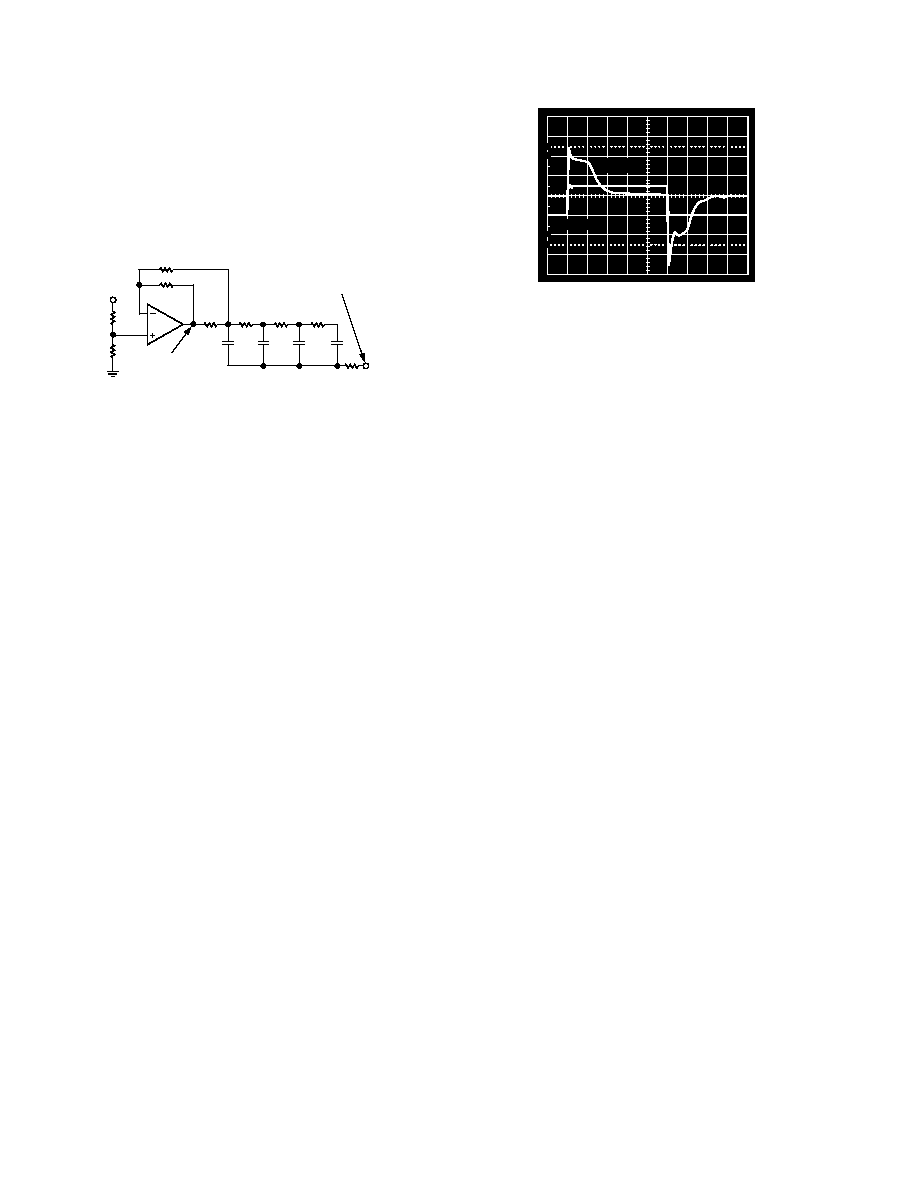
Figure 5 shows the test circuit. Series capacitors and resistors
connected to the output of the op amp represent the load of the
LCD panel. The 300
and 3 k feedback resistors are used to
improve settling time. This test circuit simulates the worst-case
scenario for a V
COM
. It drives a represented load that is connected
to a signal switched symmetrically around V
COM
. Figure 6 displays
a scope photo of the instantaneous output peak current capability
of the AD856x family.
INPUT 0V TO 8V
SQUARE WAVE WITH
15.6 s PULSEWIDTH
300
3k
10
10
10
10
10nF
10nF
10nF
10nF
MEASURE
CURRENT
4V
8V
10 20
Figure 5. V
COM
Test Circuit with Supply Voltage at 16 V
10
0%
100
90
TIME 2 s/DIV
CH 1 = 5V/DIV
CH 2 =
100mA/DIV
Figure 6. Scope Photo of the V
COM
Instantaneous
Peak Current
AD8565/AD8566/AD8567
11
REV. A
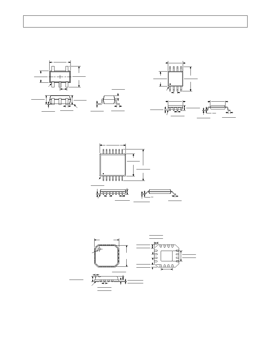
16-Terminal Leadless Frame Chip Scale
(CP-16)
16
5
13
8
9
12
1
4
BOTTOM
VIEW
0.073 (1.85)
0.067 (1.70) SQ
0.061 (1.55)
0.024 (0.60)
0.017 (0.42)
0.009 (0.24)
0.024 (0.60)
0.017 (0.42)
0.009 (0.24)
0.030 (0.75)
0.024 (0.60)
0.020 (0.50)
0.026 (0.65)
BSC
0.077 (1.95)
BSC
0.014 (0.35)
0.011 (0.28)
0.009 (0.23)
12
MAX
0.008 (0.20)
REF
0.031 (0.80) MAX
0.026 (0.65) NOM
0.002 (0.05)
0.0004 (0.01)
0.0 (0.0)
SEATING
PLANE
0.039 (1.00) MAX
0.033 (0.85) NOM
PIN 1
INDICATOR
TOP
VIEW
0.157 (4.0)
BSC SQ
0.148 (3.75)
BSC SQ
CONTROLLING DIMENSIONS ARE IN MILLIMETERS
14-Lead Thin Shrink SO
(RU-14)
14
8
7
1
0.256 (6.50)
0.246 (6.25)
0.177 (4.50)
0.169 (4.30)
PIN 1
0.201 (5.10)
0.193 (4.90)
SEATING
PLANE
0.006 (0.15)
0.002 (0.05)
0.0118 (0.30)
0.0075 (0.19)
0.0256
(0.65)
BSC
0.0433 (1.10)
MAX
0.0079 (0.20)
0.0035 (0.090)
0.028 (0.70)
0.020 (0.50)
8
0
OUTLINE DIMENSIONS
Dimensions shown in inches and (mm).
5-Lead Plastic Surface-Mount
(KS-5)
0.012 (0.30)
0.006 (0.15)
0.004 (0.10)
0.000 (0.00)
0.039 (1.00)
0.031 (0.80)
SEATING
PLANE
0.043 (1.10)
0.031 (0.80)
0.007 (0.18)
0.004 (0.10)
0.012 (0.30)
0.004 (0.10)
0.016 (0.40)
0.004 (0.10)
3
5
4
1
2
0.087 (2.20)
0.071 (1.80)
PIN 1
0.094 (2.40)
0.071 (1.80)
0.026 (0.65) BSC
0.053 (1.35)
0.045 (1.15)
8-Lead MINI_SOIC
(RM-8)
0.011 (0.28)
0.003 (0.08)
0.028 (0.71)
0.016 (0.41)
33
27
0.120 (3.05)
0.112 (2.84)
8
5
4
1
0.122 (3.10)
0.114 (2.90)
0.199 (5.05)
0.187 (4.75)
PIN 1
0.0256 (0.65) BSC
0.122 (3.10)
0.114 (2.90)
SEATING
PLANE
0.006 (0.15)
0.002 (0.05)
0.018 (0.46)
0.008 (0.20)
0.043 (1.09)
0.037 (0.94)
0.120 (3.05)
0.112 (2.84)

12
C01909
.8
10/01(A)
PRINTED IN U.S.A.
REV. A
12
AD8565/AD8566/AD8567
Revision History
Location
Page
Data Sheet changed from REV. 0 to REV. A.
Edit to 16-Lead CSP and 5-Lead SC70 Pin Configuration . . . . . . . . . . . . . . . . . . . . . . . . . . . . . . . . . . . . . . . . . . . . . . . . . . . . . . . . 1
Edit to ORDERING GUIDE . . . . . . . . . . . . . . . . . . . . . . . . . . . . . . . . . . . . . . . . . . . . . . . . . . . . . . . . . . . . . . . . . . . . . . . . . . . . . . 3
Document Outline
- Specifications
- Pinout
- Package Drawings
- Ordering Guide
- Features
- Applications
- Product Description
- Absolute Maximum Ratings
- Functional Block Diagram
- Circuit Description
- Typical Characteristics
- CAUTION
- APPLICATIONS
- DIAGRAMS
- AD856x Equivalent Input Circuit
- VCOM Test Circuit with Supply Voltage at 16 V