 | ÐлекÑÑоннÑй компоненÑ: ADG633 | СкаÑаÑÑ:  PDF PDF  ZIP ZIP |
Äîêóìåíòàöèÿ è îïèñàíèÿ www.docs.chipfind.ru
Information furnished by Analog Devices is be lieved to be accurate and
reliable. However, no responsibility is assumed by Analog Devices for its
use, nor for any infringements of patents or other rights of third parties
that may result from its use. No license is granted by implication or otherwise
under any patent or patent rights of Analog Devices. Trademarks and
registered trademarks are the property of their respective companies.
One Technology Way, P.O. Box 9106, Norwood, MA 02062-9106, U.S.A.
Tel: 781/329-4700
www.analog.com
Fax: 781/326-8703 © 2003 Analog Devices, Inc. All rights reserved.
ADG633
CMOS ±5 V/+5 V/+3 V Triple SPDT Switch
FEATURES
±2 V to ±6 V Dual Supply
2 V to 12 V Single Supply
Automotive Temperature Range 40
o
C to +125
o
C
<0.2 nA Leakage Currents
52 On Resistance over Full Signal Range
Rail-to-Rail Switching Operation
16-Lead Chip Scale/TSSOP Packages
Typical Power Consumption <0.1 W
TTL/CMOS Compatible Inputs
Package Upgrades to 74HC4053 and MAX4053/MAX4583
APPLICATIONS
Automotive Applications
Automatic Test Equipment
Data Acquisition Systems
Battery Powered Systems
Communication Systems
Audio and Video Signal Routing
Relay Replacement
Sample-and-Hold Systems
Industrial Control Systems
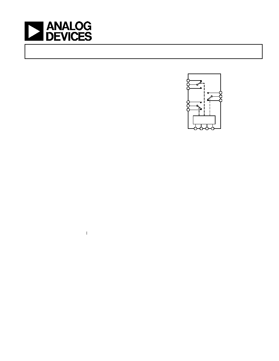
FUNCTIONAL BLOCK DIAGRAM
GENERAL DESCRIPTION
The ADG633 is a low voltage CMOS device comprising three
independently selectable SPDT (single pole double throw)
switches. They are fully specifi ed for ±5 V, +5 V, and +3 V supplies.
The ADG633 switches are turned on with a logic low (or high)
on the appropriate control input. Each switch conducts equally
well in both directions when ON and has an input signal range
that extends to the supplies. An EN input is used to enable or
EN
EN
disable the device. When disabled, all channels are switched off.
These parts are designed on an enhanced process that pro-
vides lower power dissipation yet gives high switching speeds.
Low power consumption and an operating supply range of 2 V
to 12 V make the ADG633 ideal for battery-powered portable
instruments. All channels exhibit break-before-make switching
action, preventing momentary shorting when switching chan-
nels. All digital inputs have 0.8 V to 2.4 V logic thresholds,
ensuring TTL/CMOS logic compatibility when using single
+5 V or dual ±5 V supplies.
The ADG633 is available in small 16-lead TSSOP packages and
16-lead 4 mm 4 mm chip scale packages.
PRODUCT HIGHLIGHTS
1. Single- and dual-supply operation. The ADG633 offers
high performance and is fully specifi ed and guaranteed
with ±5 V, +5 V and +3 V supply rails.
2. Automotive temperature range 40
o
C to +125
o
C.
3. Guaranteed break-before-make switching action.
4. Low power consumption, typically <0.1 W.
5. Small 16-lead TSSOP and 16-lead 4 mm 4 mm
chip scale packages.
S1B
D1
S1A
S2A
D2
S2B
S3A
D3
S3B
A0 A1 A2 EN
LOGIC
ADG633
SWITCHES SHOWN FOR A LOGIC 1 INPUT
REV. 0
2
ADG633SPECIFICATIONS
B Version Y Version
40
C
40
C
Parameter
+25
C
to +85
C
to +125
C
Unit
Test Conditions/Comments
ANALOG SWITCH
Analog Signal Range
V
SS
V
V to V
SS
SS
DD
to V
to V
V
V
DD
= +4.5 V, V
SS
= 4.5 V
On Resistance (R
ON
)
52
typ
V
S
= ±4.5 V, I
S
= 1 mA;
75
90
100
max
Test Circuit 1
On Resistance Match between
0.8
typ
Channels (R
ON
)
1.3
1.8
2
max
V
S
= +3.5 V, I
S
= 1 mA
On Resistance Flatness (R
FLAT(ON)
On Resistance Flatness (R
On Resistance Flatness (R
)
9
typ
V
DD
= +5 V, V
SS
= 5 V;
12
13
14
max
V
S
= ±3 V, I
S
= 1 mA
LEAKAGE CURRENTS
V
DD
= +5.5 V, V
SS
= 5.5 V
Source OFF Leakage I
S
(OFF)
±0.005
nA typ
V
D
= ±4.5 V, V
S
= 4.5 V;
±0.2
±5
nA max
Test Circuit 2
Drain OFF Leakage I
D
(OFF)
±0.005
nA typ
V
D
= ±4.5 V, V
S
= 4.5 V;
±0.2
±5
nA max
Test Circuit 3
Channel ON Leakage I
D
, I
S
(ON)
±0.005
nA typ
V
D
= V
S
= ±4.5 V; Test Circuit 4
±0.2
±5
nA max
DIGITAL INPUTS
Input High Voltage, V
INH
2.4
V min
Input Low Voltage, V
INL
0.8
V max
Input Current I
INL
or I
INL
INL
INH
0.005
A typ
V
IN
= V
INL
or V
INL
INL
INH
±1
A max
C
IN
, Digital Input Capacitance
2
pF typ
DYNAMIC CHARACTERISTICS
2
t
TRANS
60
ns typ
R
L
R
R = 300
L
L
, C
L
= 35 pF,
L
L
90
110
130
ns max
V
S
= 3 V; Test Circuit 5
t
ON
(EN)
70
ns typ
R
L
R
R = 300
L
L
, C
L
= 35 pF,
L
L
95
120
135
ns max
V
S
= 3 V; Test Circuit 7
t
OFF
(EN)
25
ns typ
R
L
R
R = 300
L
L
, C
L
= 35 pF,
L
L
40
45
50
ns max
V
S
= 3 V; Test Circuit 7
Break-Before-Make Time Delay, t
BBM
40
ns typ
R
L
R
R = 300
L
L
, C
L
= 35 pF,
L
L
10
ns min
V
S1
= V
S2
= 3 V; Test Circuit 6
Charge Injection
2
pC typ
V
S
= 0 V, R
S
= 0 ,
4
pC max
C
L
= 1 nF; Test Circuit 8
L
L
Off Isolation
90
dB typ
R
L
R
R = 50
L
L
, C
L
= 5 pF,
L
L
f = 1 MHz; Test Circuit 9
Total Harmonic Distortion, THD + N
0.025
% typ
R
L
R
R = 600 , 2 V p-p,
f = 20 Hz to 20 kHz
Channel-to-Channel Crosstalk
90
dB typ
R
L
R
R = 50
L
L
, C
L
= 5 pF,
L
L
f = 1 MHz; Test Circuit 11
3 dB Bandwidth
580
MHz typ
R
L
R
R = 50
L
L
, C
L
= 5 pF;
L
L
Test Circuit 10
C
S
(OFF)
4
pF typ
f = 1 MHz
C
D
(OFF)
7
pF typ
f = 1 MHz
C
D
, C
S
(ON)
12
pF typ
f = 1 MHz
POWER REQUIREMENTS
V
DD
= +5.5 V, V
SS
= 5.5 V
I
DD
0.01
A typ
Digital Inputs = 0 V or 5.5 V
1
A max
I
SS
0.01
A typ
Digital Inputs = 0 V or 5.5 V
1
A max
NOTES
1
Temperature range is as follows: B Version: 40°C to +85°C. Y Version: 40°C to +125°C.
2
Guaranteed by design, not subject to production test.
Specifi cations subject to change without notice.
DUAL SUPPLY
1
(V
DD
= +5 V ±10%, V
SS
= 5 V ±10%, GND = 0 V, unless otherwise noted.)
REV. 0
ADG633
3
SINGLE SUPPLY
1
(V
DD
= 5 V ±10%, V
SS
= 0 V, GND = 0 V, unless otherwise noted.)
B Version Y Version
40
C 40
C
Parameter
+25
C
to +85
C to +125
C Unit
Test Conditions/Comments
ANALOG SWITCH
Analog Signal Range
0 to V
DD
0 to V
0 to V
V
V
DD
= 4.5 V, V
SS
= 0 V
On Resistance (R
ON
)
85
typ
V
S
= 0 V to 4.5 V, I
S
= 1 mA;
150
160 200
max
Test Circuit 1
On Resistance Match between
4.5
typ
V
S
= +3.5 V, I
S
= 1 mA
Channels (R
ON
)
8
9 10
max
On Resistance Flatness (R
FLAT(ON)
On Resistance Flatness (R
On Resistance Flatness (R
)
13
14 16
typ
V
DD
= 5 V, V
SS
= 0 V
V
S
= 1.5 V to 4 V, I
S
= 1 mA
LEAKAGE CURRENTS
V
DD
= 5.5 V
Source OFF Leakage I
S
(OFF)
±0.005
nA typ
V
S
= 1 V/4.5 V, V
D
= 4.5 V/1 V;
±0.2
±5
nA max
Test Circuit 2
Drain OFF Leakage I
D
(OFF)
±0.005
nA typ
V
S
= 1 V/4.5 V, V
D
= 4.5 V/1 V;
±0.2
±5
nA max
Test Circuit 3
Channel ON Leakage I
D
, I
S
(ON)
±0.005
nA typ
V
S
= V
D
= 1 V or 4.5 V; Test Circuit 4
±0.2
±5
nA max
DIGITAL INPUTS
Input High Voltage, V
INH
2.4
V min
Input Low Voltage, V
INL
INL
INL
0.8
V max
Input Current I
INL
or I
INL
INL
INH
0.005
A typ
V
IN
= V
INL
or V
INL
INL
INH
±1
A max
C
IN
, Digital Input Capacitance
2
pF typ
DYNAMIC CHARACTERISTICS
2
t
TRANS
100
ns typ
R
L
R
R = 300
L
L
, C
L
= 35 pF,
L
L
150
190 220
ns max
V
S
= 3 V; Test Circuit 5
t
ON
(EN)
100
ns typ
R
L
R
R = 300
L
L
, C
L
= 35 pF,
L
L
150
190 220
ns max
V
S
= 3 V; Test Circuit 7
t
OFF
(EN)
25
ns typ
R
L
R
R = 300
L
L
, C
L
= 35 pF,
L
L
35
45 50
ns max
V
S
= 3 V; Test Circuit 7
Break-Before-Make Time Delay, t
BBM
90
ns typ
R
L
R
R = 300
L
L
, C
L
= 35 pF,
L
L
10
ns min
V
S1
= V
S2
= 3 V; Test Circuit 6
Charge Injection
0.5
pC typ
V
S
= 2.5 V, R
S
= 0 , C
L
= 1 nF;
L
L
1
pC max
Test Circuit 8
Off Isolation
90
dB typ
R
L
R
R = 50
L
L
, C
L
= 5 pF, f = 1 MHz;
L
L
Test Circuit 9
Channel-to-Channel Crosstalk
90
dB typ
R
L
R
R = 50
L
L
, C
L
= 5 pF, f = 1 MHz;
L
L
Test Circuit 11
3 dB Bandwidth
520
MHz typ
R
L
R
R = 50
L
L
, C
L
= 5 pF;
L
L
Test Circuit 10
C
S
(OFF)
5
pF typ
f = 1 MHz
C
D
(OFF)
8
pF typ
f = 1 MHz
C
D
, C
S
(ON)
12
pF typ
f = 1 MHz
POWER REQUIREMENTS
V
DD
= 5.5 V
I
DD
0.01
A typ
Digital Inputs = 0 V or 5.5 V
1
A max
NOTES
1
Temperature range is as follows: B Version: 40°C to +85°C. Y Version: 40°C to +125°C.
2
Guaranteed by design, not subject to production test.
Specifi cations subject to change without notice.
REV. 0
4
ADG633SPECIFICATIONS
SINGLE SUPPLY
1
(V
DD
= 2.7 V to 3.6 V, V
SS
= 0 V, GND = 0 V, unless otherwise noted.)
B Version Y Version
40C
40C
Parameter
+25C
to +85C
to +125C Unit Test Conditions/Comments
ANALOG SWITCH
Analog Signal Range
0 to V
DD
0 to V
0 to V V V
DD
= 2.7 V, V
SS
= 0 V
On Resistance (R
ON
)
185
typ V
S
= 0 V to 2.7 V, I
S
= 0.1 mA;
300
350
400 max Test Circuit 1
On Resistance Match between
2
typ V
S
= +1.5 V, I
S
= 0.1 mA
Channels (R
ON
)
4.5
6
7 max
LEAKAGE CURRENTS
V
DD
= 3.3 V
Source OFF Leakage I
S
(OFF)
±0.005
nA typ V
S
= 1 V/3 V, V
D
= 3 V/1 V;
±0.2
±5 nA max Test Circuit 2
Drain OFF Leakage I
D
(OFF)
±0.005
nA typ V
S
= 1 V/3 V, V
D
= 3 V/1 V;
±0.2
±5 nA max Test Circuit 3
Channel ON Leakage I
D
, I
S
(ON)
±0.005
nA typ V
S
= V
D
= 1 V or 3 V; Test Circuit 4
±0.2
±5 nA max
DIGITAL INPUTS
Input High Voltage, V
INH
2.0 V min
Input Low Voltage, V
INL
INL
INL
0.5 V max
Input Current I
INL
or I
INL
INL
INH
0.005
A typ V
IN
= V
INL
or V
INL
INL
INH
±1 A max
C
IN
, Digital Input Capacitance
2
pF typ
DYNAMIC CHARACTERISTICS
2
t
TRANS
170
ns typ R
L
R
R = 300
L
L
, C
L
= 35 pF,
L
L
300
370
400 ns max V
S
= 1.5 V; Test Circuit 5
t
ON
(EN)
200
ns typ R
L
R
R = 300
L
L
, C
L
= 35 pF,
L
L
310
380
420 ns max V
S
= 1.5 V; Test Circuit 7
t
OFF
(EN)
30
ns typ R
L
R
R = 300
L
L
, C
L
= 35 pF,
L
L
40
55
75 ns max V
S
= 1.5 V; Test Circuit 7
Break-Before-Make Time Delay, t
BBM
180
ns typ R
L
R
R = 300
L
L
, C
L
= 35 pF,
L
L
10 ns min V
S1
= V
S2
= 1.5 V; Test Circuit 6
Charge Injection
1
pC typ V
S
= 1.5 V, R
S
= 0 , C
L
= 1 nF;
L
L
2
pC max Test Circuit 8
Off Isolation
90
dB typ R
L
R
R = 50
L
L
, C
L
= 5 pF, f = 1 MHz;
L
L
Test Circuit 9
Channel-to-Channel Crosstalk
90
dB typ R
L
R
R = 50
L
L
, C
L
= 5 pF, f = 1 MHz;
L
L
Test Circuit 11
3 dB Bandwidth
500
MHz typ R
L
R
R =50
L
L
, C
L
= 5 pF;
L
L
Test Circuit 10
C
S
(OFF)
5
pF typ f = 1 MHz
C
D
(OFF)
8
pF typ f = 1 MHz
C
D
, C
S
(ON)
12
pF typ f = 1 MHz
POWER REQUIREMENTS
V
DD
= 3.3 V
I
DD
0.01
A typ Digital Inputs = 0 V or 3.3 V
1 A max
NOTES
1
Temperature range is as follows: B Version: 40°C to +85°C. Y Version: 40°C to +125°C.
2
Guaranteed by design, not subject to production test.
Specifi cations subject to change without notice.
REV. 0
ADG633
5
ABSOLUTE MAXIMUM RATINGS
1
(T
A
= 25°C, unless otherwise noted.)
V
DD
to V
SS
. . . . . . . . . . . . . . . . . . . . . . . . . . . . . . . . . . . . . . 13 V
V
DD
to GND . . . . . . . . . . . . . . . . . . . . . . . . . . 0.3 V to +13 V
V
SS
to GND . . . . . . . . . . . . . . . . . . . . . . . . . . . +0.3 V to 6.5 V
Analog Inputs
2
. . . . . . . . . . . . . . . . . .V
SS
0.3 V to V
DD
+ 0.3 V
Digital Inputs
2
. . . . . . . . . . . . . . . . GND 0.3 V to V
DD
+ 0.3 V
or 10 mA, whichever occurs fi rst
Peak Current, S or D . . . . . . . . . . . . . . . . . . . . . . . . . . . 40 mA
(Pulsed at 1 ms, 10% duty cycle max)
Continuous Current, S or D . . . . . . . . . . . . . . . . . . . . . 20 mA
Operating Temperature Range
Automotive (Y Version) . . . . . . . . . . . . . . . 40°C to +125°C
Industrial (B Version) . . . . . . . . . . . . . . . . . . 40°C to +85°C
Storage Temperature Range . . . . . . . . . . . . . . 65°C to +150°C
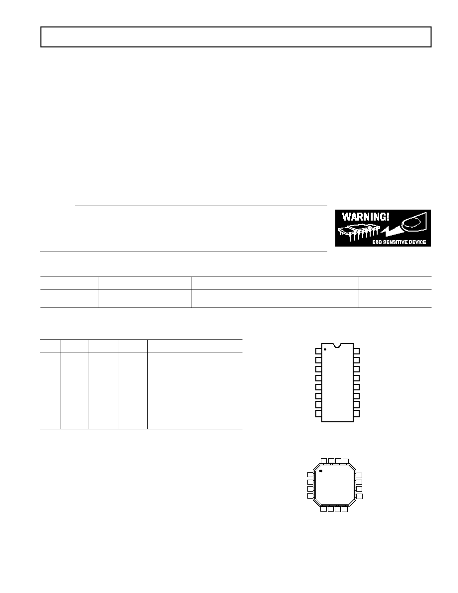
PIN CONFIGURATIONS
TSSOP
TOP VIEW
(Not to Scale)
16
15
14
13
12
11
10
9
1
2
3
4
5
6
7
S2B
S2A
S3B
D3
S3A
V
SS
EN
GND
V
DD
D2
D1
S1B
S1A
A0
A1
A2
ADG633
8
LFCSP
ADG633
TOP VIEW
(Not to Scale)
11
9
8
7
6
5
4
3
2
1
12
13
14
15
16
10
S3B
V
SS
A1
S1A
D1
S1B
EN
S3A
D3
D2
V
DD
S2A
S2B
A2
GND
A0
ORDERING GUIDE
Model
Temperature Range
Package Description
Package Option
ADG633YRU
40°C to +125°C
Thin Shrink Small Outline Package (TSSOP)
RU-16
ADG633YCP
40°C to +85°C
Chip Scale Package (LFCSP)
CP-16
Junction Temperature . . . . . . . . . . . . . . . . . . . . . . . . . . 150°C
JA
Thermal Impedance, 16-Lead TSSOP . . . . . . . . 150.4°C/W
JA
Thermal Impedance (4-Layer Board),
16-Lead LFCSP . . . . . . . . . . . . . . . . . . . . . . . . . . . 70°C/W
Lead Temperature, Soldering
Vapor Phase (60 sec) . . . . . . . . . . . . . . . . . . . . . . . . . 215°C
Infrared (15 sec) . . . . . . . . . . . . . . . . . . . . . . . . . . . . 220°C
ESD . . . . . . . . . . . . . . . . . . . . . . . . . . . . . . . . . . . . . . . . . . 4 kV
NOTES
1
Stresses above those listed under Absolute Maximum Ratings may cause permanent
damage to the device. This is a stress rating only; functional operation of the device
at these or any other conditions above those listed in the operational sections of this
specifi cation is not implied. Exposure to absolute maximum rating conditions for
extended periods may affect device reliability. Only one absolute maximum rating
may be applied at any one time.
2
Overvoltages at A
X
,
EN, S, or D will be clamped by internal diodes. Current should
be limited to the maximum ratings given.
Table I. ADG633 Truth Table
A2 A1 A0
EN
Switch Condition
X X X 1 NONE
0 0 0 0 D1S1A,
D2S2A,
D3S3A
0 0 1 0 D1S1B,
D2S2A,
D3S3A
0 1 0 0 D1S1A,
D2S2B,
D3S3A
0 1 1 0 D1S1B,
D2S2B,
D3S3A
1 0 0 0 D1S1A,
D2S2A,
D3S3B
1 0 1 0 D1S1B,
D2S2A,
D3S3B
1 1 0 0 D1S1A,
D2S2B,
D3S3B
1 1 1 0 D1S1B,
D2S2B,
D3S3B
X = Don't Care
CAUTION
ESD (electrostatic discharge) sensitive device. Electrostatic charges as high as 4000 V readily ac cu mu late
on the human body and test equipment and can discharge without detection. Although the ADG633
features proprietary ESD pro tec tion circuitry, permanent damage may occur on devices subjected to high
energy electrostatic discharges. Therefore, proper ESD pre cau tions are rec om mend ed to avoid per for mance
deg ra da tion or loss of functionality.
REV. 0
Document Outline