 | ÐлекÑÑоннÑй компоненÑ: ADG636 | СкаÑаÑÑ:  PDF PDF  ZIP ZIP |
Äîêóìåíòàöèÿ è îïèñàíèÿ www.docs.chipfind.ru
REV. 0
Information furnished by Analog Devices is believed to be accurate and
reliable. However, no responsibility is assumed by Analog Devices for its
use, nor for any infringements of patents or other rights of third parties that
may result from its use. No license is granted by implication or otherwise
under any patent or patent rights of Analog Devices.
a
ADG636
One Technology Way, P.O. Box 9106, Norwood, MA 02062-9106, U.S.A.
Tel: 781/329-4700
www.analog.com
Fax: 781/326-8703
© Analog Devices, Inc., 2002
1 pC Charge Injection, 100 pA Leakage
CMOS 5 V/+5 V/+3 V Dual SPDT Switch
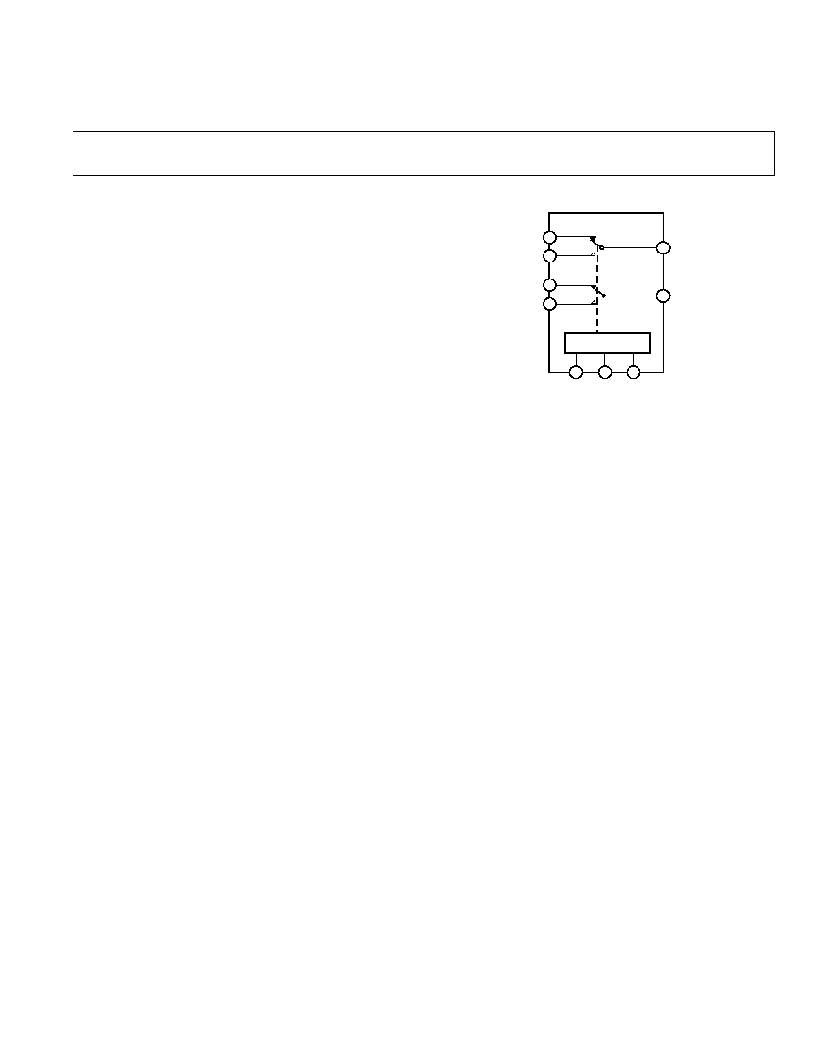
FUNCTIONAL BLOCK DIAGRAM
ADG636
S1A
D1
6
D2
9
S2B
S2A
S1B
EN
A1
A0
14
1
2
4
5
11
10
LOGIC
FEATURES
1 pC Charge Injection
2.7 V to 5.5 V Dual Supply
+2.7 V to +5.5 V Single Supply
Automotive Temperature Range: 40 C to +125 C
100 pA (Max @ 25 C) Leakage Currents
85
Typ On Resistance
Rail-to-Rail Operation
Fast Switching Times
Typical Power Consumption (<0.1 W)
TTL/CMOS Compatible Inputs
14-Lead TSSOP Package
APPLICATIONS
Automatic Test Equipment
Data Acquisition Systems
Battery-Powered Instruments
Communication Systems
Sample-and-Hold Systems
Remote Powered Equipment
Audio and Video Signal Routing
Relay Replacement
Avionics
GENERAL DESCRIPTION
The ADG636 is a monolithic device, comprising two independently
selectable CMOS SPDT (Single Pole, Double Throw) switches.
When on, each switch conducts equally well in both directions.
The ADG636 operates from a dual
±2.7 V to ±5.5 V supply, or
from a single supply of +2.7 V to +5.5 V.
This switch offers ultralow charge injection of
±1.5 pC over the
entire signal range and leakage current of 10 pA typical at 25
°C.
It offers on-resistance of 85
typ, which is matched to within
2
between channels. The ADG636 also has low power dissi-
pation yet gives high switching speeds.
The ADG636 exhibits break-before-make switching action and
is available in a 14-lead TSSOP package.
PRODUCT HIGHLIGHTS
1. Ultralow Charge Injection (Q
INJ
:
± 1.5 pC typ over full
signal range)
2. Leakage Current <0.25 nA max @ 85
°C
3. Dual
±2.7 V to ±5 V or Single +2.7 V to +5.5 V Supply
4. Automotive Temperature Range: 40
°C to +125°C
5. Small 14-Lead TSSOP Package

REV. 0
2
ADG636SPECIFICATIONS
40 C to
40 C to
Parameter
+25 C
+85 C
+125 C
Unit
Test Conditions/Comments
ANALOG SWITCH
Analog Signal Range
V
SS
to V
DD
V
V
DD
= +4.5 V, V
SS
= 4.5 V
On Resistance (R
ON
)
85
typ
V
S
=
±3 V, I
S
= 1 mA,
115
140
160
max
Test Circuit 1
On Resistance Match Between
Channels (DR
ON
)
2
typ
V
S
=
±3 V, I
S
= 1 mA
4
5.5
6.5
max
On Resistance Flatness (R
FLAT(ON)
)
25
typ
V
S
=
±3 V, I
S
= 1 mA
40
55
60
max
LEAKAGE CURRENTS
V
DD
= +5.5 V, V
SS
= 5.5 V
Source OFF Leakage I
S
(OFF)
±0.01
nA typ
V
S
=
±4.5 V, V
D
= 4.5 V,
±0.1
±0.25
± 2
nA max
Test Circuit 2
Drain OFF Leakage I
D
(OFF)
±0.01
nA typ
V
S
=
±4.5 V, V
D
= 4.5 V,
±0.1
±0.25
± 2
nA max
Test Circuit 2
Channel ON Leakage I
D,
I
S
(ON)
±0.01
nA typ
V
S
= V
D
=
± 4.5 V, Test Circuit 3
±0.1
±0.25
± 6
nA max
DIGITAL INPUTS
Input High Voltage, V
INH
2.4
V min
Input Low Voltage, V
INL
0.8
V max
Input Current
I
INL
or I
INH
0.005
µA typ
V
IN
= V
INL
or V
INH
±0.1
µA max
C
IN
, Digital Input Capacitance
2
pF typ
DYNAMIC CHARACTERISTICS
2
Transition Time
70
ns typ
V
S1A
= +3 V, V
S1B
= 3 V, R
L
= 300
,
100
120
150
ns max
C
L
= 35 pF, Test Circuit 4
t
ON
Enable
100
ns typ
R
L
= 300
, C
L
= 35 pF
135
170
190
ns max
V
S
= 3 V, Test Circuit 5
t
OFF
Enable
55
ns typ
R
L
= 300
, C
L
= 35 pF
80
90
100
ns max
V
S
= 3 V, Test Circuit 5
Break-Before-Make Time Delay, t
BBM
20
ns typ
R
L
= 300
, C
L
= 35 pF,
10
ns min
V
S
= 3 V, Test Circuit 5
Charge Injection
1.2
pC typ
V
S
= 0 V, R
S
= 0
, C
L
= 1 nF,
Test Circuit 7
Off Isolation
65
dB typ
R
L
= 50
, C
L
= 5 pF, f = 10 MHz,
Test Circuit 8
Channel-to-Channel Crosstalk
65
dB typ
R
L
= 50
, C
L
= 5 pF, f = 10 MHz,
Test Circuit 10
Bandwidth 3 dB
610
MHz typ
R
L
= 50
, C
L
= 5 pF, Test Circuit 9
C
S
(OFF)
5
pF typ
f = 1 MHz
C
D
(OFF)
8
pF typ
f = 1 MHz
C
D,
C
S
(ON)
8
pF typ
f = 1 MHz
POWER REQUIREMENTS
V
DD
= +5.5 V, V
SS
= 5.5 V
I
DD
0.001
µA typ
Digital Inputs = 0 V or 5.5 V
1.0
µA max
I
SS
0.001
µA typ
Digital Inputs = 0 V or 5.5 V
1.0
µA max
NOTES
1
Y Version Temperature Range: 40
°C to +125°C
2
Guaranteed by design, not subject to production test.
Specifications subject to change without notice.
DUAL SUPPLY
1
(V
DD
= 5 V 10%, V
SS
= 5 V 10%, GND = 0 V. All specifications 40 C to +125 C unless noted.)

REV. 0
3
ADG636
40 C to
40 C to
Parameter
+25 C
+85 C
+125 C
Unit
Test Conditions/Comments
ANALOG SWITCH
Analog Signal Range
0 V to V
DD
V
V
DD
= 4.5 V, V
SS
= 0 V
On Resistance (R
ON
)
210
typ
V
S
= 3.5 V, I
S
= 1 mA,
290
350
380
max
Test Circuit 1
On Resistance Match Between
Channels (
R
ON
)
3
typ
V
S
= 3.5 V, I
S
= 1 mA
12
13
max
LEAKAGE CURRENTS
V
DD
= 5.5 V
Source OFF Leakage I
S
(OFF)
±0.01
nA typ
V
S
= 1 V/4.5 V, V
D
= 4.5 V/1 V,
±0.1
±0.25
±2
nA max
Test Circuit 2
Drain OFF Leakage I
D
(OFF)
±0.01
nA typ
V
S
= 1 V/4.5 V, V
D
= 4.5 V/1 V
±0.1
±0.25
±2
nA max
Test Circuit 2
Channel ON Leakage I
D
, I
S
(ON)
±0.01
nA typ
V
S
= V
D
= 4.5 V/1 V,
±0.1
±0.25
±6
nA max
Test Circuit 3
DIGITAL INPUTS
Input High Voltage, V
INH
2.4
V min
Input Low Voltage, V
INL
0.8
V max
Input Current
I
INL
or I
INH
0.005
µA typ
V
IN
= V
INL
or V
INH
±0.1
µA max
C
IN
, Digital Input Capacitance
2
pF typ
DYNAMIC CHARACTERISTICS
2
Transition Time
90
ns typ
V
S1A
= 3 V, V
S1B
= 0 V, R
L
= 300
,
150
185
210
ns max
C
L
= 35 pF, Test Circuit 4
t
ON
Enable
135
ns typ
R
L
= 300
, C
L
= 35 pF
180
235
275
ns max
V
S
= 3 V, Test Circuit 5
t
OFF
Enable
70
ns typ
R
L
= 300
, C
L
= 35 pF
105
120
135
ns max
V
S
= 3 V, Test Circuit 5
Break-Before-Make Time Delay, t
BBM
30
ns typ
R
L
= 300
, C
L
= 35 pF,
10
ns min
V
S
= 3 V, Test Circuit 5
Charge Injection
0.3
pC typ
V
S
= 0 V, R
S
= 0
, C
L
= 1 nF,
Test Circuit 7
Off Isolation
60
dB typ
R
L
= 50
, C
L
= 5 pF, f = 10 MHz,
Test Circuit 8
Channel-to-Channel Crosstalk
65
dB typ
R
L
= 50
, C
L
= 5 pF, f = 10 MHz,
Test Circuit 10
Bandwidth 3 dB
530
MHz typ
R
L
= 50
, C
L
= 5 pF, Test Circuit 9
C
S
(OFF)
5
pF typ
f = 1 MHz
C
D
(OFF)
8
pF typ
f = 1 MHz
C
D,
C
S
(ON)
8
pF typ
f = 1 MHz
POWER REQUIREMENTS
V
DD
= 5.5 V
Digital Inputs = 0 V or 5.5 V
I
DD
0.001
µA typ
1.0
µA max
NOTES
1
Y Version Temperature Range: 40
°C to +125°C
2
Guaranteed by design, not subject to production test.
Specifications subject to change without notice.
(V
DD
= 5 V 10%, V
SS
= 0 V, GND = 0 V. All specifications 40 C to +125 C unless otherwise noted.)
SINGLE SUPPLY
1

REV. 0
ADG636
4
40 C to
40 C to
Parameter
+25 C
+85 C
+125 C
Unit
Test Conditions/Comments
ANALOG SWITCH
Analog Signal Range
0 V to V
DD
V
V
DD
= 2.7 V, V
SS
= 0 V
On Resistance (R
ON
)
380
420
460
typ
V
S
= 1.5 V, I
S
= 1 mA, Test Circuit 1
On Resistance Match Between
Channels (
R
ON
)
5
typ
V
S
= 1.5 V, I
S
= 1 mA
LEAKAGE CURRENTS
V
DD
= 3.3 V
Source OFF Leakage I
S
(OFF)
±0.01
nA typ
V
S
= 1 V/3 V, V
D
= 3 V/1 V,
±0.1
±0.25
±2
nA max
Test Circuit 2
Drain OFF Leakage I
D
(OFF)
±0.01
nA typ
V
S
= 1 V/3 V, V
D
= 3 V/1 V,
±0.1
±0.25
±2
nA max
Test Circuit 2
Channel ON Leakage I
D
, I
S
(ON)
±0.01
nA typ
V
S
= V
D
= 1 V/3 V,
±0.1
±0.25
±6
nA max
Test Circuit 3
DIGITAL INPUTS
Input High Voltage, V
INH
2.0
V min
Input Low Voltage, V
INL
0.8
V max
Input Current
I
INL
or I
INH
0.005
µA typ
V
IN
= V
INL
or V
INH
±0.1
µA max
C
IN
, Digital Input Capacitance
2
pF typ
DYNAMIC CHARACTERISTICS
2
Transition Time
170
ns typ
V
S1A
= 2 V, V
S1B
= 0 V, R
L
= 300
,
320
390
450
ns max
C
L
= 35 pF, Test Circuit 4
t
ON
Enable
250
ns typ
R
L
= 300
, C
L
= 35 pF
360
460
530
ns max
V
S
= 2 V, Test Circuit 6
t
OFF
Enable
110
ns typ
R
L
= 300
, C
L
= 35 pF
175
205
230
ns max
V
S
= 2 V, Test Circuit 6
Break-Before-Make Time Delay, t
BBM
80
ns typ
R
L
= 300
, C
L
= 35 pF,
10
ns min
V
S1
= 2 V, Test Circuit 5
Charge Injection
0.6
pC typ
V
S
= 0 V, R
S
= 0
, C
L
= 1 nF,
Test Circuit 7
Off Isolation
60
dB typ
R
L
= 50
, C
L
= 5 pF, f = 10 MHz,
Test Circuit 8
Channel-to-Channel Crosstalk
65
dB typ
R
L
= 50
, C
L
= 5 pF, f = 10 MHz,
Test Circuit 10
Bandwidth 3 dB
530
MHz typ
R
L
= 50
, C
L
= 5 pF, Test Circuit 9
C
S
(OFF)
5
pF typ
f = 1 MHz
C
D
(OFF)
8
pF typ
f = 1 MHz
C
D,
C
S
(ON)
8
pF typ
f = 1 MHz
POWER REQUIREMENTS
V
DD
= 3.3 V
Digital Inputs = 0 V or 3.3 V
I
DD
0.001
µA typ
1.0
µA max
NOTES
1
Y Version Temperature Range: 40
°C to +125°C
2
Guaranteed by design, not subject to production test.
Specifications subject to change without notice.
(V
DD
= 3 V 10%, V
SS
= 0 V, GND = 0 V. All specifications 40 C to +125 C unless otherwise noted.)
SINGLE SUPPLY
1
REV. 0
ADG636
5
CAUTION
ESD (electrostatic discharge) sensitive device. Electrostatic charges as high as 4000 V readily
accumulate on the human body and test equipment and can discharge without detection. Although
the ADG636 features proprietary ESD protection circuitry, permanent damage may occur on
devices subjected to high-energy electrostatic discharges. Therefore, proper ESD precautions are
recommended to avoid performance degradation or loss of functionality.
WARNING!
ESD SENSITIVE DEVICE
ABSOLUTE MAXIMUM RATINGS
1
(T
A
= 25
°C unless otherwise noted)
V
DD
to V
SS
. . . . . . . . . . . . . . . . . . . . . . . . . . . . . . . . . . . . 13 V
V
DD
to GND . . . . . . . . . . . . . . . . . . . . . . . . 0.3 V to +6.5 V
V
SS
to GND . . . . . . . . . . . . . . . . . . . . . . . . . +0.3 V to 6.5 V
Analog Inputs
2
. . . . . . . . . . . . . . . . V
SS
0.3 V to V
DD
+ 0.3 V
Digital Inputs
2
. . . . . . . . . . . . . . . . 0.3 V to V
DD
+ 0.3 V or
30 mA, Whichever Occurs First
Peak Current, S or D
(Pulsed at 1 ms, 10% Duty Cycle max) . . . . . . . . . . 20 mA
Continuous Current, S or D . . . . . . . . . . . . . . . . . . . . 10 mA
Operating Temperature Range
Automotive (Y Version) . . . . . . . . . . . . . . 40
°C to +125°C
Storage Temperature Range . . . . . . . . . . . . 65
°C to +150°C
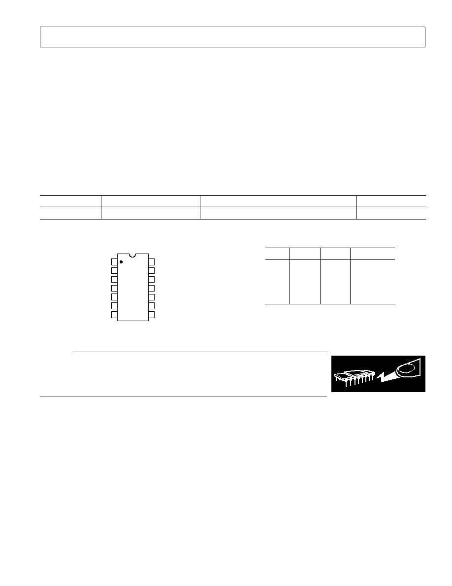
Table I. Truth Table
A1
A0
EN
ON Switch
X
X
0
NONE
0
0
1
S1A, S2A
0
1
1
S1B, S2A
1
0
1
S1A, S2B
1
1
1
S1B, S2B
ORDERING GUIDE
Model
Temperature Range
Package Description
Package Option
ADG636YRU
40
°C to +125°C
Thin Shrink Small Outline (TSSOP)
RU-14
Junction Temperature . . . . . . . . . . . . . . . . . . . . . . . . . 150
°C
TSSOP Package
JA
Thermal Impedance . . . . . . . . . . . . . . . . . . . . 150
°C/W
JC
Thermal Impedance . . . . . . . . . . . . . . . . . . . . . 27
°C/W
Lead Temperature, Soldering (10 seconds) . . . . . . . . . . 300
°C
IR Reflow, Peak Temperature . . . . . . . . . . . . . . . . . . 220
°C
NOTES
1
Stresses above those listed under Absolute Maximum Ratings may cause
permanent damage to the device. This is a stress rating only; functional operation
of the device at these or any other conditions above those listed in the operational
sections of this specification is not implied. Exposure to absolute maximum rating
conditions for extended periods may affect device reliability. Only one absolute
maximum rating may be applied at any one time.
2
Overvoltages at EN, A0, A1, S, or D will be clamped by internal diodes. Current
should be limited to the maximum ratings given.
PIN CONFIGURATION
A0
EN
V
SS
S1A
S1B
D1
NC
1
A1
GND
V
DD
S2A
S2B
D2
NC
ADG636
2
3
4
5
6
7
14
13
12
11
10
9
8
TOP VIEW
(Not To Scale)
NC = NO CONNECT

REV. 0
ADG636
6
TERMINOLOGY
V
DD
Most Positive Power Supply Potential
V
SS
Most Negative Power Supply in a Dual Supply Application. In single supply applications, this should be tied to
ground at the device.
GND
Ground (0 V) Reference
I
DD
Positive Supply Current
I
SS
Negative Supply Current
S
Source Terminal. May be an input or output.
D
Drain Terminal. May be an input or output.
R
ON
Ohmic Resistance between D and S
R
ON
On Resistance Match between any two channels (i.e., R
ON
max R
ON
min)
R
FLAT(ON)
Flatness is defined as the difference between the maximum and minimum value of On Resistance as measured
over the specified analog signal range.
I
S
(OFF)
Source Leakage Current with the Switch "OFF"
I
D
(OFF)
Drain Leakage Current with the Switch "OFF"
I
D
, I
S
(ON)
Channel Leakage Current with the Switch "ON"
V
D
, V
S
Analog Voltage on Terminals D, S
V
INL
Maximum Input Voltage for Logic "0"
V
INH
Minimum Input Voltage for Logic "1"
I
INL
(I
INH
)
Input Current of the Digital Input
C
S
(OFF)
Channel Input Capacitance for "OFF" condition.
C
D
(OFF)
Channel Output Capacitance for "OFF" condition.
C
D
, C
S
(ON)
"ON" Switch Capacitance
C
IN
Digital Input Capacitance
t
ON
(EN)
Delay time between the 50% and 90% points of the digital input and Switch "ON" condition
t
OFF
(EN)
Delay time between the 50% and 90% points of the digital input and Switch "OFF" condition
t
TRANSITION
Delay time between the 50% and 90% points of the digital input and Switch "ON" condition when switching
from one address state to another.
t
BBM
"OFF" time or "ON" time measured between the 80% points of both switches, when switching from one address
state to another.
Charge Injection
A measure of the Glitch Impulse transferred from the Digital Input to the Analog Output during switching.
Crosstalk
A measure of unwanted signal that is coupled through from one channel to another as a result of parasitic
capacitance.
Off Isolation
A measure of unwanted signal coupling through an "OFF" switch.
Bandwidth
The Frequency Response of the "ON" Switch
Insertion Loss
Loss Due to the On Resistance of the Switch
REV. 0
ADG636
7
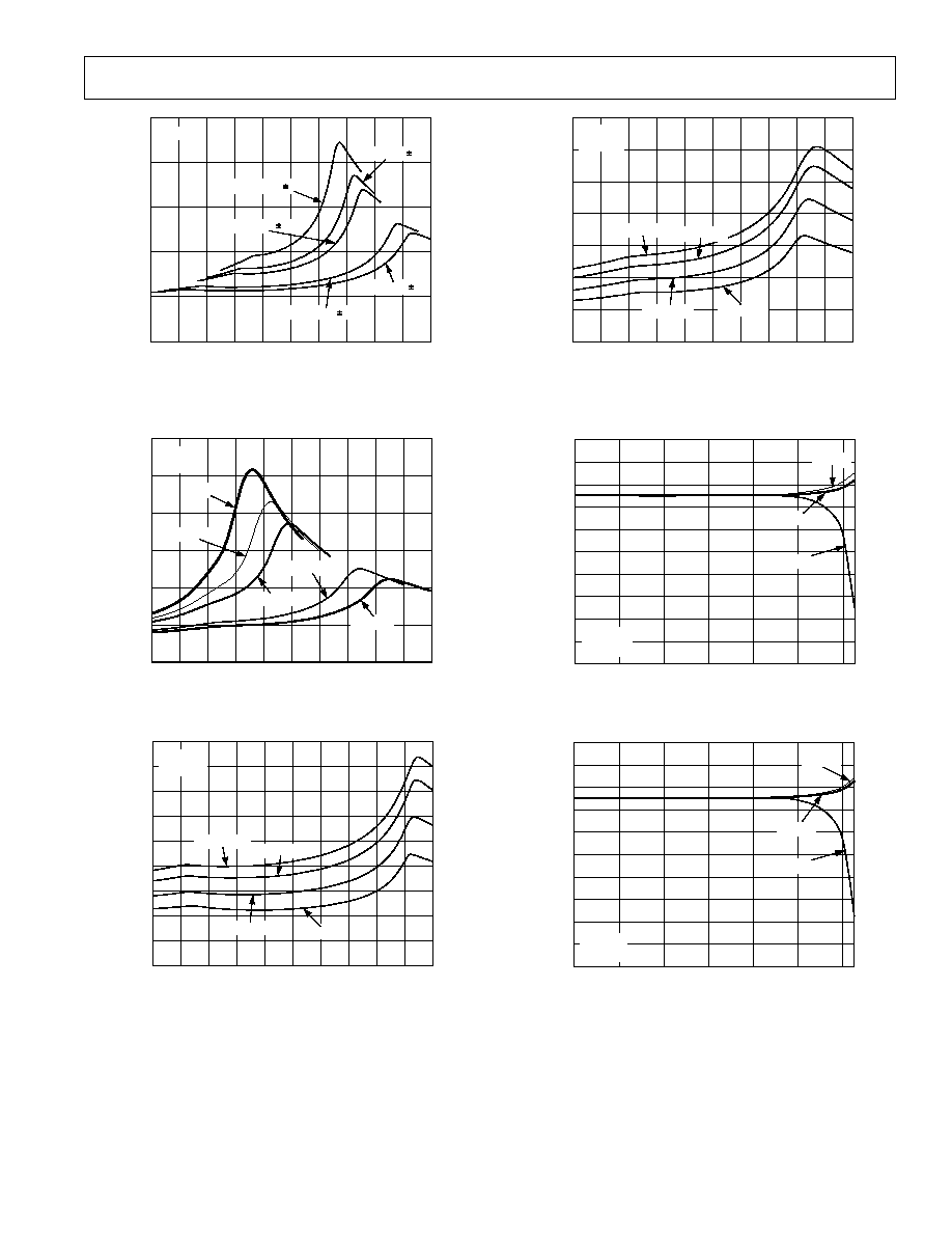
0
250
V
D
, V
S
V
5
ON RESIST
ANCE
100
2
2
5
200
150
50
4
3
1
0
1
3
4
T
A
= 25 C
V
DD
, V
SS
= 2.5V
V
DD
, V
SS
= 3V
V
DD
, V
SS
= 3.3V
V
DD
, V
SS
= 4.5V
V
DD
, V
SS
= 5V
TPC 1. On Resistance vs. V
D
(V
S
). Dual Supply
0
600
V
D
, V
S
V
0
ON RESIST
ANCE
300
1.5
3.5
5.0
500
400
200
0.5
1.0
2.0
2.5
3.0
4.0
4.5
100
V
DD
= 3V
V
DD
= 2.7V
T
A
= 25 C
V
SS
= 0V
V
DD
= 3.3V
V
DD
= 4.5V
V
DD
= 5V
TPC 2. On Resistance vs. V
D
(V
S
). Single Supply
0
180
V
D
, V
S
V
ON RESIST
ANCE
80
140
120
60
20
V
DD
= +5V
V
SS
= 5V
160
100
40
5
2
2
5
4
3
1
0
1
3
4
T
A
= +125 C
T
A
= +85 C
T
A
= +25 C
T
A
= 40 C
TPC 3. On Resistance vs. V
D
(V
S
) for Different
Temperatures. Dual Supply
0
350
V
D
, V
S
V
0
ON RESIST
ANCE
150
1.5
3.5
5.0
300
200
100
0.5
1.0
2.0
2.5
3.0
4.0
4.5
50
V
DD
= 5V
V
SS
= 0V
250
T
A
= +125 C
T
A
= +85 C
T
A
= +25 C
T
A
= 40 C
TPC 4. On Resistance vs. V
D
(V
S
) for Different
Temperatures. Single Supply
15
5
TEMPERATURE C
0
CURRENT
nA
3
3
1
5
20
40
60
80
7
1
100
120
V
DD
= +5V
V
SS
= 5V
13
11
9
I
S
(OFF)
I
D
(OFF)
I
D
, I
S
(ON)
TPC 5. Leakage Currents vs. Temperatures. Dual Supply
15
5
TEMPERATURE C
0
CURRENT
nA
3
3
1
5
20
40
60
80
7
1
100
120
V
DD
= 5V
V
SS
= 0V
13
11
9
I
D
(OFF)
I
S
(OFF)
I
D
, I
S
(ON)
TPC 6. Leakage Currents vs. Temperature. Single Supply
Typical Performance Characteristics
REV. 0
ADG636
8
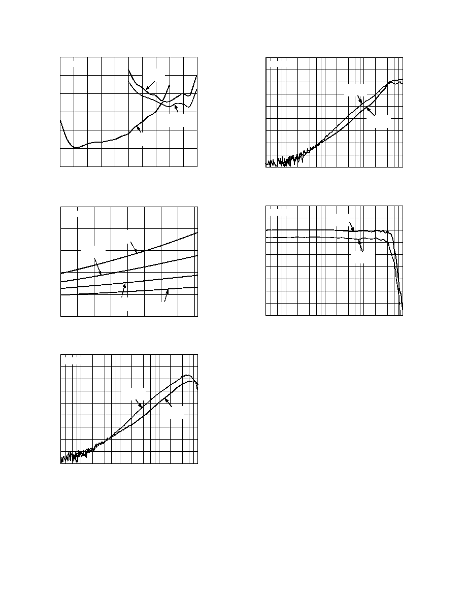
2.0
1.0
V
S
V
5
CHARGE INJECTION
pC
0.5
4
2
0
1
0
3
5
1.5
1.0
0.5
3
1
2
4
V
DD
= 5V
V
SS
= 0V
V
DD
= 3V
V
SS
= 0V
V
DD
= +5V
V
SS
= 5V
T
A
= 25 C
TPC 7. Charge Injection vs. Source Voltage
0
250
TEMPERATURE C
40
TIME
ns
20
20
60
80
200
120
50
100
150
0
40
100
T
A
= 25 C
V
DD
= +5V
V
SS
= 5V
V
DD
= +5V
V
SS
= 5V
V
DD
= 5V
V
SS
= 0V
V
DD
= 5V
V
SS
= 0V
t
ON
t
OFF
TPC 8. t
ON
/t
OFF
Enable Timing vs. Temperature
90
80
70
60
50
40
30
20
10
0
FREQUENCY MHz
0.3
1
10
100
1000
A
TTENU
A
TION
dB
T
A
= 25 C
V
DD
= +5V
V
SS
= 0V
V
DD
= +5V
V
SS
= 5V
TPC 9. Off Isolation vs. Frequency
90
80
70
60
50
40
30
20
10
0
FREQUENCY MHz
0.3
10
100
1000
A
TTENU
A
TION
dB
1
T
A
= 25 C
V
DD
= +5V
V
SS
= 0V
V
DD
= +5V
V
SS
= 5V
TPC 10. Crosstalk vs. Frequency
18
16
14
12
10
8
6
4
2
0
FREQUENCY MHz
0.3
1
10
100
1000
A
TTENU
A
TION
dB
T
A
= 25 C
V
DD
= +5V
V
SS
= 5V
V
DD
= +5V
V
SS
= 0V
TPC 11. On Response vs. Frequency
REV. 0
ADG636
9
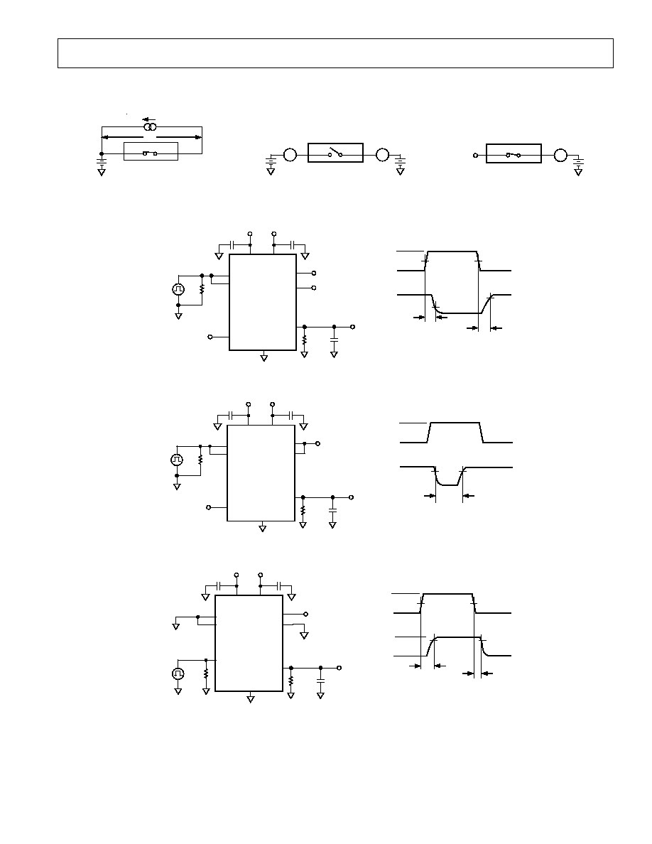
Test Circuits
V
S
V
DD
V
DD
EN
A0
A1
50
2.4V
0.1 F
S1A
V
SS
GND
D1
V
SS
V
S1A
V
OUT
R
L
300
C
L
35pF
S1B
0.1 F
V
S1B
50%
50%
90%
90%
ADDRESS
DRIVE (V
IN
)
V
OUT
t
TRANSITION
0V
3V
t
TRANSITION
Test Circuit 4. Transition Time, t
TRANSITION
V
S
V
DD
V
DD
EN
A1
A0
50
2.4V
0.1 F
S1A
V
SS
GND
D1
V
SS
V
S
V
OUT
R
L
300
C
L
35pF
S1B
0.1 F
t
BBM
80%
80%
ADDRESS
DRIVE (V
IN
)
V
OUT
0V
3V
Test Circuit 5. Break-Before-Make Delay, t
BBM
V
DD
V
DD
EN
A1
A0
0.1 F
S1A
V
SS
GND
D1
V
SS
V
S
V
OUT
R
L
300
C
L
35pF
S1B
0.1 F
V
S
50
50%
50%
0.9V
0
0.9V
0
ENABLE
DRIVE (V
IN
)
OUTPUT
t
ON
(EN)
0V
3V
t
OFF
(EN)
V
0
0V
Test Circuit 6. Enable Delay, t
ON
(EN), t
OFF
(EN)
I
DS
V1
S
D
R
ON
= V1/I
DS
V
S
Test Circuit 1. On Resistance
S
D
V
S
A
A
V
D
I
S
(OFF)
I
D
(OFF)
Test Circuit 2. Off Leakage
S
D
A
V
D
I
D
(ON)
NC
Test Circuit 3. On Leakage
REV. 0
ADG636
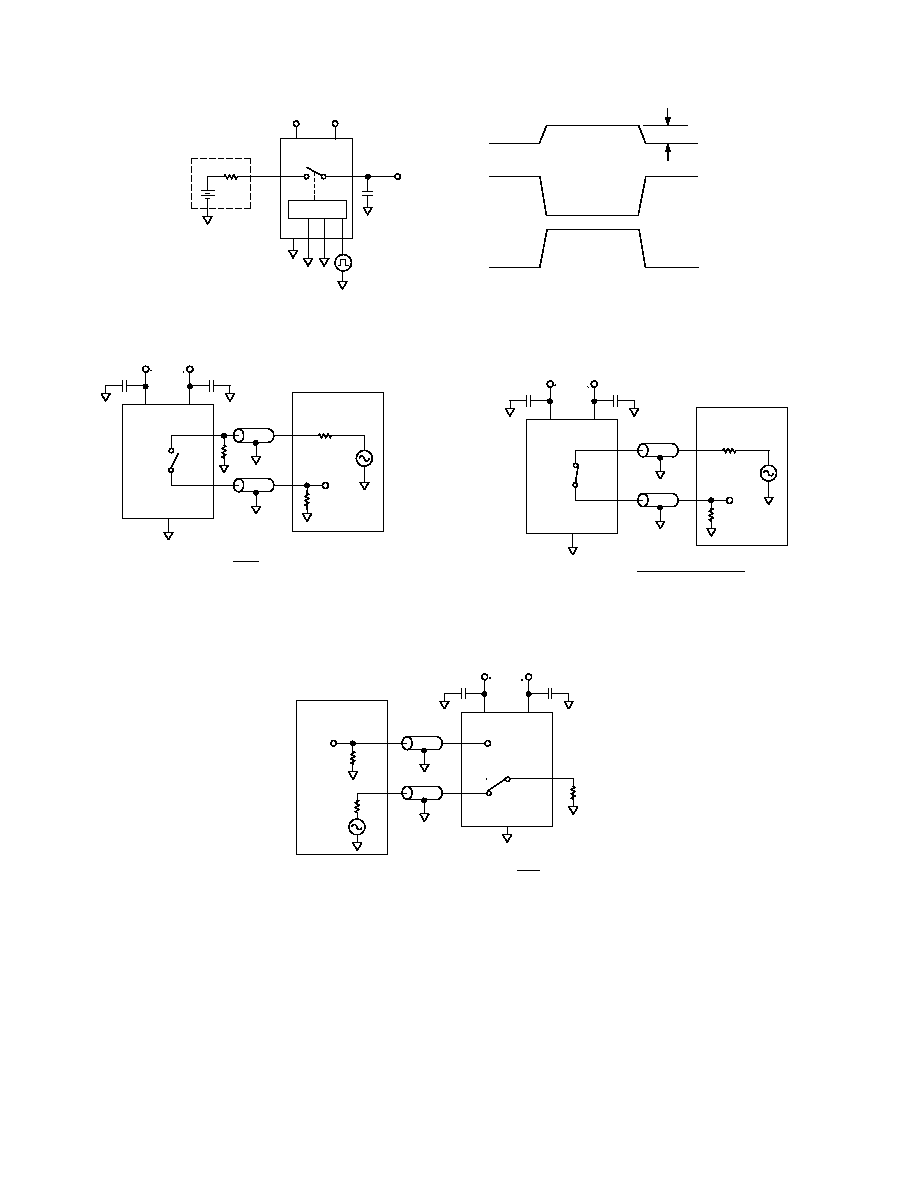
10
S
D
V
DD
V
S
GND
C
L
1nF
V
OUT
R
S
V
DD
SW ON
V
IN
SW OFF
V
OUT
Q
INJ
= C
L
V
OUT
V
OUT
V
SS
V
SS
SW ON
V
IN
SW OFF
SW ON
SW OFF
SW OFF
CHARGE INJECTION =
V
OUT
C
L
DECODER
A2
A1
EN
Test Circuit 7. Charge Injection
V
S
V
OUT
50
NETWORK
ANALYZER
GND
V
DD
S
D
50
OFF
ISOLATION
=
20
LOG
V
OUT
V
S
0.1 F
0.1 F
V
SS
V
DD
V
SS
R
L
50
Test Circuit 8. Off Isolation
GND
V
DD
D
CHANNEL-TO-CHANNEL CROSSTALK = 20 LOG
V
OUT
V
S
0.1 F
0.1 F
V
SS
V
DD
V
SS
R
L
50
NETWORK
ANALYZER
V
OUT
V
S
50
S1
S2
R
L
50
Test Circuit 10. Channel-to-Channel Crosstalk
V
S
V
OUT
50
NETWORK
ANALYZER
GND
V
DD
S
D
INSERTION LOSS = 20 LOG
V
OUT
WITH SWITCH
V
OUT
WITHOUT SWITCH
0.1 F
0.1 F
V
SS
V
DD
V
SS
R
L
50
Test Circuit 9. Bandwidth
REV. 0
ADG636
11
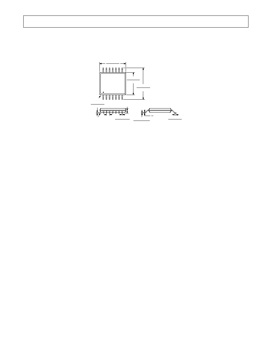
14-Lead TSSOP Package
(RU-14)
14
8
7
1
0.256 (6.50)
0.246 (6.25)
0.177 (4.50)
0.169 (4.30)
PIN 1
0.201 (5.10)
0.193 (4.90)
SEATING
PLANE
0.006 (0.15)
0.002 (0.05)
0.0118 (0.30)
0.0075 (0.19)
0.0256
(0.65)
BSC
0.0433 (1.10)
MAX
0.0079 (0.20)
0.0035 (0.090)
0.028 (0.70)
0.020 (0.50)
8
0
OUTLINE DIMENSIONS
Dimensions shown in inches and (mm).

12
C0275401/02(0)
PRINTED IN U.S.A.