 | ÐлекÑÑоннÑй компоненÑ: ADG658 | СкаÑаÑÑ:  PDF PDF  ZIP ZIP |
Äîêóìåíòàöèÿ è îïèñàíèÿ www.docs.chipfind.ru
Information furnished by Analog Devices is be lieved to be accurate and
reliable. However, no responsibility is assumed by Analog Devices for its
use, nor for any infringements of patents or other rights of third parties
that may result from its use. No license is granted by implication or oth-
erwise under any patent or patent rights of Analog Devices. Trademarks
and registered trademarks are the property of their respective companies.
One Technology Way, P.O. Box 9106, Norwood, MA 02062-9106, U.S.A.
Tel: 781/329-4700
www.analog.com
Fax: 781/326-8703 © 2003 Analog Devices, Inc. All rights reserved.
ADG658/ADG659
+3 V/+5 V/±5 V CMOS 4-/8-Channel
Analog Multiplexers
FEATURES
±2 V to ±6 V Dual Supply
2 V to 12 V Single Supply
Automotive Temperature Range 40
o
C to +125
o
C
<0.1 nA Leakage Currents
45 On Resistance over Full Signal Range
Rail-to-Rail Switching Operation
Single 8-to-1 Multiplexer ADG658
Differential 4-to-1 Multiplexer ADG659
16-Lead LFCSP/TSSOP Packages
Typical Power Consumption <0.1 W
TTL/CMOS Compatible Inputs
Package Upgrades to 74HC4051/74HC4052 and
MAX4051/MAX4052/MAX4581/MAX4582
APPLICATIONS
Automotive Applications
Automatic Test Equipment
Data Acquisition Systems
Battery-Powered Systems
Communication Systems
Audio and Video Signal Routing
Relay Replacement
Sample-and-Hold Systems
Industrial Control Systems
FUNCTIONAL BLOCK DIAGRAM
S1
S8
S1A
S4B
S4A
D
DB
DA
A0
A1
EN
A0
A1
EN
A2
1 OF 8
DECODER
1 OF 4
DECODER
SWITCHES SHOWN FOR A LOGIC 1 INPUT
ADG658
ADG659
S1B
GENERAL DESCRIPTION
The ADG658 and ADG659 are low voltage, CMOS analog
multiplexers comprised of eight single channels and four dif-
ferential channels, respectively. The ADG658 switches one of
eight inputs (S1S8) to a common output, D, as determined by
the 3-bit binary address lines A0, A1, and A2. The ADG659
switches one of four differential inputs to a common differential
output, as determined by the 2-bit binary address lines A0 and
A1. An EN input on both devices is used to enable or disable
EN
EN
the device. When disabled, all channels are switched off.
These parts are designed on an enhanced process that provides
lower power dissipation yet gives high switching speeds. These
parts can operate equally well as either multiplexers or demulti-
plexers and have an input range that extends to the supplies. All
channels exhibit break-before-make switching action, prevent-
ing momentary shorting when switching channels. All digital
inputs have 0.8 V to 2.4 V logic thresholds, ensuring TTL/
CMOS logic compatibility when using single +5 V or dual
±5 V supplies.
The ADG658 and ADG659 are available in 16-lead TSSOP
packages and 16-lead 4 mm 4 mm LFCSP packages.
PRODUCT HIGHLIGHTS
1. Single- and dual-supply operation. The ADG658 and
ADG659 offer high performance and are fully specifi ed
and guaranteed with ±5 V, +5 V, and +3 V supply rails.
2. Automotive temperature range 40
o
C to +125
o
C.
3. Low power consumption, typically <0.1 W.
4. 16-lead 4 mm 4 mm LFCSP packages and 16-lead
TSSOP package.
REV. 0
2
ADG658/ADG659SPECIFICATIONS
B Version Y Version
40C
40C
Parameter
+25C
to +85C
to +125C
Unit
Test Conditions/Comments
ANALOG SWITCH
Analog Signal Range
V
SS
to V
DD
V
V
DD
= +4.5 V, V
SS
= 4.5 V
On Resistance (R
ON
)
45
typ
V
S
= ±4.5 V, I
S
= 1 mA;
75
90
100
max
Test Circuit 1
On Resistance Match between
1.3
typ
Channels (
Channels (
Channels ( R
ON
)
3
3.2
3.5
max
V
S
= 3.5 V, I
S
= 1 mA
On Resistance Flatness (R
FLAT(ON)
)
10
typ
V
DD
= +5 V, V
SS
= 5 V;
16
17
18
max
V
S
= ±3 V, I
S
= 1 mA
LEAKAGE CURRENTS
V
DD
= +5.5 V, V
SS
= 5.5 V
Source OFF Leakage I
S
(OFF)
±0.005
nA typ
V
D
= ±4.5 V, V
S
= 4.5 V;
±0.2
±5
nA max
Test Circuit 2
Drain OFF Leakage I
D
(OFF)
±0.005
nA typ
V
D
= ±4.5 V, V
S
= 4.5 V;
ADG658
±0.2
±5
nA max
Test Circuit 3
ADG659
±0.1
±2.5
nA max
Channel ON Leakage I
D
, I
S
(ON)
±0.005
nA typ
V
D
= V
S
= ±4.5 V; Test Circuit 4
ADG658
±0.2
±5
nA max
ADG659
±0.1
±2.5
nA max
DIGITAL INPUTS
Input High Voltage, V
INH
2.4
V min
Input Low Voltage, V
INL
0.8
V max
Input Current
I
INL
or I
INL
INL
INH
0.005
µA typ
V
IN
= V
INL
or V
INL
INL
INH
±1
µA max
C
IN
, Digital Input Capacitance
2
pF typ
DYNAMIC CHARACTERISTICS
2
t
TRANS
80
ns typ
R
L
= 300
L
L
, C
L
= 35 pF
L
L
115
140
165
ns max
V
S
= 3 V; Test Circuit 5
t
ON
(EN)
80
ns typ
R
L
= 300
L
L
, C
L
= 35 pF
L
L
115
140
165
ns max
V
S
= 3 V; Test Circuit 7
t
OFF
(EN)
30
ns typ
R
L
= 300
L
L
, C
L
= 35 pF
L
L
45
50
55
ns max
V
S
= 3 V; Test Circuit 7
Break-Before-Make Time Delay, t
BBM
50
ns typ
R
L
= 300
L
L
, C
L
= 35 pF
L
L
10
ns min
V
S1
= V
S2
= 3 V; Test Circuit 6
Charge Injection
2
pC typ
V
S
= 0 V, R
S
= 0 ,
4
pC max
C
L
= 1 nF; Test Circuit 8
L
L
Off Isolation
90
dB typ
R
L
= 50
L
L
, C
L
= 5 pF,
L
L
f = 1 MHz; Test Circuit 9
Total Harmonic Distortion, THD + N
0.025
% typ
R
L
R
R = 600 , 2 V p-p,
f = 20 Hz to 20 kHz
Channel-to-Channel Crosstalk
90
dB typ
R
L
= 50
L
L
, C
L
= 5 pF,
L
L
(ADG659)
f = 1 MHz; Test Circuit 11
3 dB Bandwidth
ADG658
210
MHz typ
R
L
= 50
L
L
, C
L
= 5 pF;
L
L
ADG659
400
MHz typ
Test Circuit 10
C
S
(OFF)
4
pF typ
f = 1 MHz
C
D
(OFF)
ADG658
23
pF typ
f = 1 MHz
ADG659
12
pF typ
f = 1 MHz
C
D
, C
S
(ON)
ADG658
28
pF typ
f = 1 MHz
ADG659
16
pF typ
f = 1 MHz
POWER REQUIREMENTS
V
DD
= +5.5 V, V
SS
= 5.5 V
I
DD
0.01
µA typ
Digital Inputs = 0 V or 5.5 V
1
µA max
I
SS
0.01
µA typ
Digital Inputs = 0 V or 5.5 V
1
µA max
NOTES
1
Temperature range is as follows: B Version: 40°C to +85°C. Y Version: 40°C to +125°C.
2
Guaranteed by design, not subject to production test.
Specifi cations subject to change without notice.
DUAL SUPPLY
1
(V
DD
= +5 V ±10%, V
SS
= 5 V ±10%, GND = 0 V, unless otherwise noted.)
REV. 0
ADG658/ADG659
3
SINGLE SUPPLY
1
(V
DD
= 5 V ±10%, V
SS
= 0 V, GND = 0 V, unless otherwise noted.)
B Version Y Version
40C
40C
Parameter
+25C
to +85C
to +125C
Unit
Test Conditions/Comments
ANALOG SWITCH
Analog Signal Range
0 to V
DD
0 to V
0 to V
V
V
DD
= 4.5 V, V
SS
= 0 V
On Resistance (R
ON
)
85
typ
V
S
= 0 V to 4.5 V, I
S
= 1 mA;
150
160
200
max
Test Circuit 1
On Resistance Match between
4.5
typ
V
S
= 3.5 V, I
S
= 1 mA
Channels (
Channels (
Channels ( R
ON
)
8
9
10
max
On Resistance Flatness (R
FLAT(ON)
)
13
14
16
typ
V
DD
= 5 V, V
SS
= 0 V
V
S
= 1.5 V to 4 V, I
S
= 1 mA
LEAKAGE CURRENTS
V
DD
= 5.5 V
Source OFF Leakage I
S
(OFF)
±0.005
nA typ
V
S
= 1 V/4.5 V, V
D
= 4.5 V/1 V;
±0.2
±5
nA max
Test Circuit 2
Drain OFF Leakage I
D
(OFF)
±0.005
nA typ
V
S
= 1 V/4.5 V, V
D
= 4.5 V/1 V;
ADG658
±0.2
±5
nA max
Test Circuit 3
ADG659
±0.1
±2.5
nA max
Channel ON Leakage I
D
, I
S
(ON)
±0.005
nA typ
V
S
= V
D
= 1 V or 4.5 V, Test Circuit 4
ADG658
±0.2
±5
nA max
ADG659
±0.1
±2.5
nA max
DIGITAL INPUTS
Input High Voltage, V
INH
2.4
V min
Input Low Voltage, V
INL
INL
INL
0.8
V max
Input Current
I
INL
or I
INL
INL
INH
0.005
µA typ
V
IN
= V
INL
or V
INL
INL
INH
±1
µA max
C
IN
, Digital Input Capacitance
2
pF typ
DYNAMIC CHARACTERISTICS
2
t
TRANS
120
ns typ
R
L
= 300
L
L
, C
L
= 35 pF
L
L
200
270
300
ns max
V
S
= 3 V; Test Circuit 5
t
ON
(EN)
120
ns typ
R
L
= 300
L
L
, C
L
= 35 pF
L
L
190
245
280
ns max
V
S
= 3 V; Test Circuit 7
t
OFF
(EN)
35
ns typ
R
L
= 300
L
L
, C
L
= 35 pF
L
L
50
60
70
ns max
V
S
= 3 V; Test Circuit 7
Break-Before-Make Time Delay, t
BBM
100
ns typ
R
L
= 300
L
L
, C
L
= 35 pF
L
L
10
ns min
V
S1
= V
S2
= 3 V; Test Circuit 6
Charge Injection
0.5
pC typ
V
S
= 2.5 V, R
S
= 0 , C
L
= 1 nF;
L
L
1
pC max
Test Circuit 8
Off Isolation
90
dB typ
R
L
= 50
L
L
, C
L
= 5 pF, f = 1 MHz;
L
L
Test Circuit 9
Channel-to-Channel Crosstalk
90
dB typ
R
L
= 50
L
L
, C
L
= 5 pF; f = 1 MHz;
L
L
(
ADG659)
Test Circuit 11
3 dB Bandwidth
ADG658
180
MHz typ
R
L
= 50
L
L
, C
L
= 5 pF;
L
L
ADG659
330
MHz typ
Test Circuit 10
C
S
(OFF)
5
pF typ
f = 1 MHz
C
D
(OFF)
ADG658
29
pF typ
f = 1 MHz
ADG659
15
pF typ
f = 1 MHz
C
D
, C
S
(ON)
ADG658
30
pF typ
f = 1 MHz
ADG659
16
pF typ
f = 1 MHz
POWER REQUIREMENTS
V
DD
= 5.5 V
I
DD
0.01
µA typ
Digital Inputs = 0 V or 5.5 V
1
µA max
NOTES
1
Temperature range is as follows: B Version: 40°C to +85°C. Y Version: 40°C to +125°C.
2
Guaranteed by design, not subject to production test.
Specifi cations subject to change without notice.
REV. 0
4
ADG658/ADG659SPECIFICATIONS
SINGLE SUPPLY
1
(V
DD
= 2.7 V to 3.6 V, V
SS
= 0 V, GND = 0 V, unless otherwise noted.)
B Version Y Version
40C
40C
Parameter
+25C
to +85C
to +125C
Unit
Test Conditions/Comments
ANALOG SWITCH
Analog Signal Range
0 to V
DD
V
V
DD
= 2.7 V, V
SS
= 0 V
On Resistance (R
ON
)
185
typ
V
S
= 0 V to 2.7 V, I
S
= 0.1 mA;
300
350
400
max
Test Circuit 1
On Resistance Match between
2
typ
V
S
= 1.5 V, I
S
= 0.1 mA
Channels (
Channels (
Channels ( R
ON
)
4.5
6
7
max
LEAKAGE CURRENTS
V
DD
= 3.3 V
Source OFF Leakage I
S
(OFF)
±0.005
nA typ
V
S
= 1 V/3 V, V
D
= 3 V/1 V;
±0.2
±5
nA max
Test Circuit 2
Drain OFF Leakage I
D
(OFF)
±0.005
nA typ
V
S
= 1 V/3 V, V
D
= 3 V/1 V;
ADG658
±0.2
±5
nA max
Test Circuit 3
ADG659
±0.1
±2.5
nA max
Channel ON Leakage I
D
, I
S
(ON)
±0.005
nA typ
V
S
= V
D
= 1 V or 3 V; Test Circuit 4
ADG658
±0.2
±5
nA max
ADG659
±0.1
±2.5
nA max
DIGITAL INPUTS
Input High Voltage, V
INH
2.0
V min
Input Low Voltage, V
INL
INL
INL
0.5
V max
Input Current
I
INL
or I
INL
INL
INH
0.005
µA typ
V
IN
= V
INL
or V
INL
INL
INH
±1
µA max
C
IN
, Digital Input Capacitance
2
pF typ
DYNAMIC CHARACTERISTICS
2
t
TRANS
200
ns typ
R
L
= 300
L
L
, C
L
= 35 pF
L
L
370
440
490
ns max
V
S
= 1.5 V; Test Circuit 7
t
ON
(EN)
230
ns typ
R
L
= 300
L
L
, C
L
= 35 pF
L
L
370
440
490
ns max
V
S
= 1.5 V; Test Circuit 7
t
OFF
(EN)
50
ns typ
R
L
= 300
L
L
, C
L
= 35 pF
L
L
80
90
110
ns max
V
S
= 1.5 V; Test Circuit 7
Break-Before-Make Time Delay, t
BBM
200
ns typ
R
L
= 300
L
L
, C
L
= 35 pF
L
L
10
ns min
V
S1
= V
S2
= 1.5 V; Test Circuit 6
Charge Injection
1
pC typ
V
S
= 1.5 V, R
S
= 0 , C
L
= 1 nF;
L
L
2
pC max
Test Circuit 8
Off Isolation
90
dB typ
R
L
= 50
L
L
, C
L
= 5 pF, f = 1 MHz;
L
L
Test Circuit 9
Channel-to-Channel Crosstalk
90
dB typ
R
L
= 50
L
L
, C
L
= 5 pF, f = 1 MHz;
L
L
(
ADG659)
Test Circuit 11
3 dB Bandwidth
ADG658
160
MHz typ
R
L
= 50
L
L
, C
L
= 5 pF;
L
L
ADG659
300
MHz typ
Test Circuit 10
C
S
(OFF)
5
pF typ
f = 1 MHz
C
D
(OFF)
ADG658
29
pF typ
f = 1 MHz
ADG659
15
pF typ
f = 1 MHz
C
D
, C
S
(ON)
ADG658
30
pF typ
f = 1 MHz
ADG659
16
pF typ
f = 1 MHz
POWER REQUIREMENTS
V
DD
= 3.6 V
I
DD
0.01
µA typ
Digital Inputs = 0 V or 3.6 V
1
µA max
NOTES
1
Temperature range is as follows:
B Version: 40°C to +85°C. Y Version: 40°C to +125°C.
2
Guaranteed by design, not subject to production test.
Specifi cations subject to change without notice.
REV. 0
ADG658/ADG659
5
ABSOLUTE MAXIMUM RATINGS
1
(T
A
= 25°C, unless otherwise noted.)
V
DD
to V
SS
. . . . . . . . . . . . . . . . . . . . . . . . . . . . . . . . . . .13 V
V
DD
to GND . . . . . . . . . . . . . . . . . . . . . . . 0.3 V to +13 V
V
SS
to GND . . . . . . . . . . . . . . . . . . . . . . . .+0.3 V to 6.5 V
Analog Inputs
2
. . . . . . . . . . . . . . V
SS
0.3 V to V
DD
+ 0.3 V
Digital Inputs
2
. . . . . . . . . . . . GND 0.3 V to V
DD
+ 0.3 V
or 10 mA, whichever occurs fi rst
Peak Current, S or D . . . . . . . . . . . . . . . . . . . . . . . 40 mA
(Pulsed at 1 ms, 10% duty cycle max)
Continuous Current, S or D . . . . . . . . . . . . . . . . . 20 mA
Operating Temperature Range
Automotive (Y Version) . . . . . . . . . . . . 40°C to +125°C
Industrial (B Version) . . . . . . . . . . . . . . 40°C to +85°C
Storage Temperature Range . . . . . . . . . . 65°C to +150°C
Junction Temperature . . . . . . . . . . . . . . . . . . . . . . . 150°C
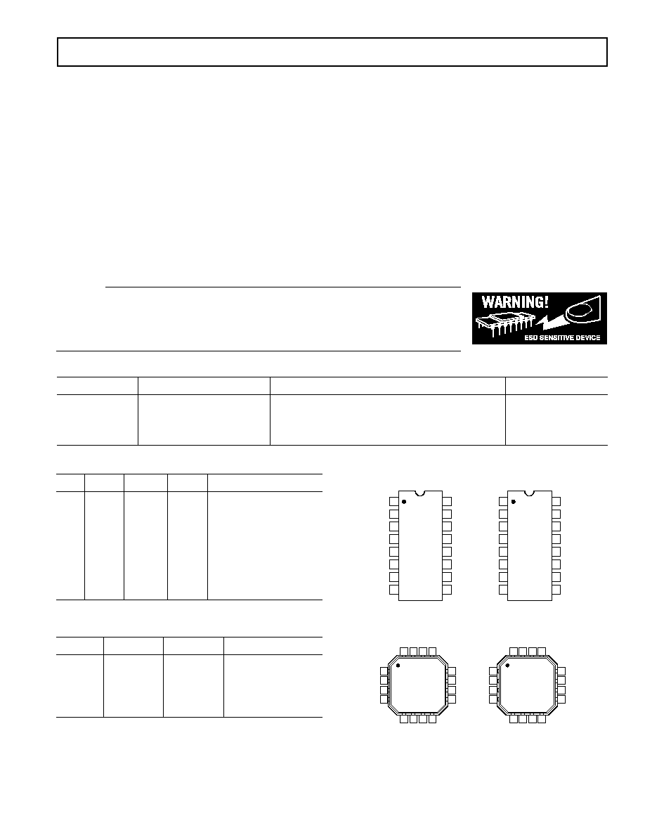
PIN CONFIGURATIONS
TSSOP
ADG659
TOP VIEW
(Not to Scale)
ADG658
TOP VIEW
(Not to Scale)
1
2
3
4
5
6
7
8
1
2
3
4
5
6
7
8
16
15
14
13
12
11
10
9
16
15
14
13
12
11
10
9
V
DD
S3
S2
S1
S4
A0
A1
A2
V
DD
S3A
S2A
DA
S1A
S4A
A0
A1
S1B
S3B
DB
S4B
S2B
EN
V
SS
GND
S5
S7
D
S8
S6
EN
V
SS
GND
LFCSP
12
11
10
9
1
2
3
4
16 15 14 13
5
6
7
8
D
S8
S6
EN
V
SS
GND
A2
A1
S2
S1
S4
A0
S7
S5
V
DD
S3
ADG659
TOP VIEW
(Not to Scale)
12
11
10
9
1
2
3
4
16 15 14 13
5
6
7
8
DB
S4B
S2B
EN
V
SS
GND
A1
A0
S2A
DA
S1A
S4A
S3B
S1B
V
DD
S3A
ADG658
TOP VIEW
(Not to Scale)
ORDERING GUIDE
Model
Temperature Range
Package Description
Package Option
ADG658YRU
40°C to +125°C
Thin Shrink Small Outline Package (TSSOP)
RU-16
ADG658YCP
40°C to +85°C
Lead Frame Chip Scale Package (LFCSP)
CP-16
ADG659YRU
40°C to +125°C
Thin Shrink Small Outline Package (TSSOP)
RU-16
ADG659YCP
40°C to +85°C
Lead Frame Chip Scale Package (LFCSP)
CP-16
JA
Thermal Impedance, 16-Lead TSSOP . . . . . 150.4°C/W
JA
Thermal Impedance (4-Layer Board),
16-Lead LFCSP . . . . . . . . . . . . . . . . . . . . . . . . 70°C/W
Lead Temperature, Soldering
Vapor Phase (60 sec) . . . . . . . . . . . . . . . . . . . . . . . 215°C
Infrared (15 sec) . . . . . . . . . . . . . . . . . . . . . . . . . . 220°C
ESD . . . . . . . . . . . . . . . . . . . . . . . . . . . . . . . . . . . . . 5.5 kV
NOTES
1
Stresses above those listed under Absolute Maximum Ratings may cause perma-
nent damage to the device. This is a stress rating only; functional operation of
the device at these or any other conditions above those listed in the operational
sections of this specifi cation is not implied. Exposure to absolute maximum
rating conditions for extended periods may affect device reliability. Only one
absolute maximum rating may be applied at any one time.
2
Overvoltages at A
X,
EN, S, or D will be clamped by internal diodes. Current
should be limited to the maximum ratings given.
Table I. ADG658 Truth Table
A2 A1 A0
EN
Switch Condition
X X X 1 NONE
0 0 0 0 1
0 0 1 0 2
0 1 0 0 3
0 1 1 0 4
1 0 0 0 5
1 0 1 0 6
1 1 0 0 7
1 1 1 0 8
X = Don't Care
Table II. ADG659 Truth Table
A1 A0
EN
On Switch Pair
X X 1 NONE
0 0 0 1
0 1 0 2
1 0 0 3
1 1 0 4
X = Don't Care
CAUTION
ESD (electrostatic discharge) sensitive device. Electrostatic charges as high as 4000 V readily ac cu mu late
on the human body and test equipment and can discharge without detection. Although the ADG658/
ADG659 feature proprietary ESD pro tec tion circuitry, permanent damage may occur on devices subjected
to high energy electrostatic discharges. Therefore, proper ESD pre cau tions are rec om mend ed to avoid
per for mance deg ra da tion or loss of functionality.
REV. 0

ADG658/ADG659
6
TERMINOLOGY
Parameter Description
V
DD
Most Positive Power Supply Potential.
V
SS
Most Negative Power Supply Potential.
I
DD
Positive Supply Current.
I
SS
Negative Supply Current.
GND
Ground (0 V) Reference.
S
Source Terminal. May be an input or output.
D
Drain Terminal. May be an input or output.
A
X
Logic Control Input.
EN
Active Low Digital Input. When high, device is disabled and all switches are OFF. When low, A
X
logic inputs
determine ON switch.
V
D
(V
S
)
Analog Voltage on Terminals D, S.
R
ON
Ohmic Resistance between D and S.
R
ON
On Resistance Match between Any Two Channels, i.e., R
ON
max R
ON
min.
R
FLAT(ON)
R
R
Flatness is defi ned as the difference between the maximum and minimum value of ON Resistance as
measured over the specifi ed analog signal range.
I
S
(OFF)
Source Leakage Current with the Switch OFF.
I
D
(OFF)
Drain Leakage Current with the Switch OFF.
I
D
, I
S
(ON)
Channel Leakage Current with the Switch ON.
V
INL
Maximum Input Voltage for Logic 0.
V
INH
Minimum Input Voltage for Logic 1.
I
INL
(I
INH
)
Input Current of the Digital Input.
C
S
(OFF)
OFF Switch Source Capacitance. Measured with reference to ground.
C
D
(OFF)
OFF Switch Drain Capacitance. Measured with reference to ground.
C
D
, C
S
(ON)
ON Switch Capacitance. Measured with reference to ground.
C
IN
Digital Input Capacitance.
t
ON
Delay between Applying the Digital Control Input and the Output Switching ON. See Test Circuit 7.
t
OFF
Delay between Applying the Digital Control Input and the Output Switching OFF.
t
BBM
ON Time. Measured between 80% points of both switches when switching from one address state to another.
Charge Injection Measure of the Glitch Impulse Transferred from the Digital Input to the Analog Output during Switching.
Off Isolation
Measure of Unwanted Signal Coupling through an OFF Switch.
Crosstalk
Measure of Unwanted Signal Coupled through from One Channel to Another as a Result of Parasitic Capacitance.
Bandwidth
The Frequency at which the Output is Attenuated by 3 dB.
On Response
The Frequency Response of the ON Switch.
Insertion Loss
The Loss Due to the ON Resistance of the Switch.
Charge Injection
REV. 0
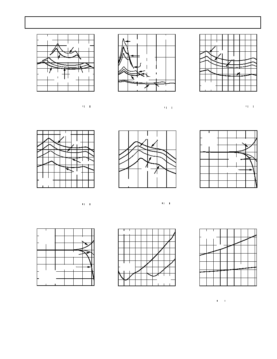
Typical Performance CharacteristicsADG658/ADG659
7
0
200
150
100
50
250
0
2
4
6
8
10
12
T
A
= 25C
V
DD
= 2.7V
V
DD
= 3V
V
DD
= 3.3V
V
DD
= 4.5V
V
DD
= 5V
V
DD
= 5.5V
V
DD
= 10V
V
DD
= 12V
V
D
, V
S
V
ON RESISTANCE
TPC 2. On Resistance vs. V
D
TPC 2. On Resistance vs. V
TPC 2. On Resistance vs. V (V
D
D
S
(V
(V )
for Single Supply
0
200
150
100
50
250
0
0.5
1.0
1.5
2.0
2.5
3.0
300
+125C
+85C
V
D
, V
S
V
ON RESISTANCE
+25C
40C
V
DD
= 3V
V
SS
= 0V
TPC 5. On Resistance vs. V
D
TPC 5. On Resistance vs. V
TPC 5. On Resistance vs. V (V
D
D
S
(V
(V )
for Different Temperatures
(Single Supply)
4
12
8
4
0
5
3
1
1
3
5
10
6
2
2
14
4
2
0
2
4
V
S
V
Q
INJ
P
C
V
DD
= 5V
V
SS
= 5V
V
DD
= 5V
V
SS
= 0V
T
A
= 25C
TPC 8. Charge Injection vs.
Source Voltage
0
80
60
40
20
100
5.5
3.5
1.5
0.5
2.5
4.5
70
50
30
10
90
V
DD
, V
SS
= 2.7V
T
A
= 25C
V
DD
, V
SS
= 3V
V
DD
, V
SS
= 5.5V
V
DD
, V
SS
= 5V
V
DD
, V
SS
= 4.5V
V
D
, V
S
V
ON RESISTANCE
TPC 1. On Resistance vs. V
D
TPC 1. On Resistance vs. V
TPC 1. On Resistance vs. V (V
D
D
S
(V
(V )
for Dual Supply
100
60
20
140
0
1.0
2.0
80
40
0
120
0.5
1.5
2.5 3.0
4.5
4.0
5.0
+125C
+85C
+25C
40C
V
DD
= 5V
V
SS
= 0V
3.5
V
D
, V
S
V
ON RESISTANCE
TPC 4. On Resistance vs. V
D
TPC 4. On Resistance vs. V
TPC 4. On Resistance vs. V (V
D
D
S
(V
(V )
for Different Temperatures
(Single Supply)
0.5
0.5
1.5
2.5
1.5
0
1.0
2.0
1.0
0
20
40
60
80
100
120
TEMPERATURE C
CURRENT nA
V
DD
= 5V
V
SS
= 0V
V
D
= 4V
V
S
= 1V
I
S
(OFF)
I
D
(OFF)
I
S
, I
D
(ON)
V
DD
= 3V
V
SS
= 0V
V
D
= 2.4V
V
S
= 1V
TPC 7. Leakage Currents vs.
Temperature (Single Supply)
0
80
60
40
20
100
5
2
0
70
50
30
10
90
4
1
1
2
3
5
V
D
, V
S
V
ON RESISTANCE
+125C
+85C
+25C
40C
V
DD
= 5V
V
SS
= 5V
4
3
TPC 3. On Resistance vs. V
D
TPC 3. On Resistance vs. V
TPC 3. On Resistance vs. V (V
D
D
S
(V
(V )
for Different Temperatures
(Dual Supply)
0.5
0.5
1.5
2.5
1.5
0
1.0
2.0
1.0
0
20
40
60
80
100
120
TEMPERATURE C
CURRENT nA
V
DD
= 5V
V
SS
= 5V
V
D
= 4V
V
S
= 4V
I
S
(OFF)
I
D
(OFF)
I
S
, I
D
(ON)
TPC 6. Leakage Currents vs.
Temperature (Dual Supply)
100
60
20
140
80
40
0
120
40 20
0
20
40
60
80 100 120
TEMPERATURE C
TIME ns
V
DD
= +5V
V
SS
= 5V
t
ON
t
OFF
TPC 9. t
ON
/t
ON
ON OFF
Times vs.
OFF
OFF
Temperature (Dual Supply)
REV. 0
8
ADG658/ADG659
300
200
100
250
150
0
350
40 20
0
20
40
60
80 100 120
50
V
SS
= 0V
TEMPERATURE C
TIME ns
t
ON
t
OFF
V
DD
= 3V
V
DD
= 3V
V
DD
= 5V
V
DD
= 5V
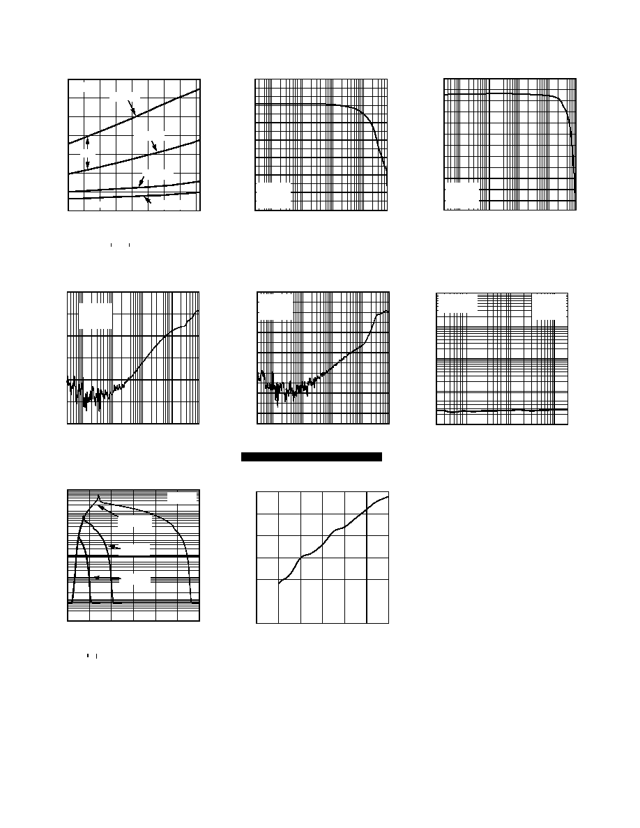
TPC 10. t
ON
/t
ON
ON OFF
Times vs.
OFF
OFF
Temperature (Single Supply)
100k
1M
10M
100M
40
80
120
0
60
100
20
FREQUENCY Hz
dB
V
DD
= +5V
V
SS
= 5V
T
A
= 25C
TPC 13. OFF Isolation vs. Frequency
100
1
0.01
10000
10
0.1
1000
0
2
4
6
8
10
12
V
SS
= 0V
V
DD
= 12V
V
DD
= 5V
V
DD
= 3V
V(EN) V
I
DD
A
TPC 16. V
DD
TPC 16. V
TPC 16. V Current vs. Logic Level
DD
DD
100k
1M
10M
100M
9
11
13
0
10
12
15
7
14
FREQUENCY Hz
dB
8
6
4
5
3
1
2
V
DD
= +5V
V
SS
= 5V
T
A
= 25C
TPC 11. ON Response vs.
Frequency (ADG658)
30
70
110
0
50
90
130
100k
1M
10M
100M
40
80
120
10
60
100
20
FREQUENCY Hz
dB
V
DD
= 5V
V
SS
= +5V
T
A
= 25C
0
2.5
2.0
1.5
1.0
3.0
0
2
4
6
8
10
12
0.5
V
DD
V
LOGIC THRESHOLD VOLTAGE
V
TPC 17. Logic Threshold
Voltage vs. Supply Voltage
100k
1M
10M
100M
12
16
20
0
14
18
24
8
22
FREQUENCY Hz
dB
10
6
2
4
V
DD
= +5V
V
SS
= 5V
T
A
= 25C
TPC 12. ON Response vs.
Frequency (ADG659)
100
20
50 100
FREQUENCY Hz
THD + N
%
200 500 1k
5k 10k 20k
10
1
0.1
0.01
2k
600
IN AND OUT
V
DD
= +5V
V
SS
= 5V
T
A
= 25C
TPC 15. THD + Noise
REV. 0
ADG658/ADG659
9
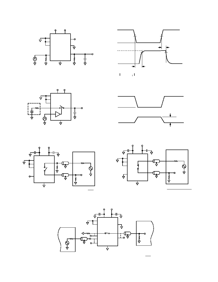
Test Circuits
I
DS
V1
S
D
V
S
R
ON
= V
1
/I
DS
Test Circuit 1. On Resistance
V
DD
S1
D
V
D
V
SS
V
S
V
DD
V
SS
S2
S8
GND
EN
LOGIC 1
A
I
S
(OFF)
Test Circuit 2. I
S
Test Circuit 2. I
Test Circuit 2. I (OFF)
S
S
V
DD
V
SS
V
S1
V
S8
V
OUT
50
R
L
300
V
IN
A2
A1
A0
EN
GND
S1
S8
D
ADG658*
90%
90%
50%
50%
3V
0V
V
S1
V
OUT
V
S8
V
DD
V
SS
*SIMILAR CONNECTION FOR ADG659
C
L
35pF
S2 THRU S7
ADDRESS
DRIVE (V
IN
)
t
TRANSITION
t
TRANSITION
Test Circuit 5. Switching Time of Multiplexer, t
TRANSITION
V
DD
V
SS
V
S
V
OUT
V
IN
A2
A1
A0
EN
GND
S1
S2 THRU S7
S8
D
ADG658*
t
BBM
80%
3V
0V
V
OUT
*SIMILAR CONNECTION FOR ADG659
80%
ADDRESS
DRIVE (V
IN
)
V
DD
V
SS
50
R
L
300
C
L
35pF
Test Circuit 6. Break-Before-Make Delay, t
BBM
Test Circuit 6. Break-Before-Make Delay, t
Test Circuit 6. Break-Before-Make Delay, t
V
DD
S1
D
V
S
V
SS
V
O
S2
S8
GND
EN
LOGIC 1
A
I
D
(OFF)
V
DD
V
SS
Test Circuit 3. I
D
Test Circuit 3. I
Test Circuit 3. I (OFF)
D
D
V
DD
S1
D
V
S
V
SS
V
D
S8
GND
EN
A
I
D
(ON)
V
DD
V
SS
Test Circuit 4. I
D
Test Circuit 4. I
Test Circuit 4. I (ON)
REV. 0
ADG658/ADG659
10
V
DD
V
SS
V
S
V
OUT
50
A2
A1
A0
EN
GND
S1
S2S8
D
t
ON
(EN)
0.9V
O
50%
50%
3V
0V
V
O
0V
V
IN
0.9V
O
ENABLE
DRIVE (V
IN
)
OUTPUT
t
OFF
(EN)
V
SS
ADG658*
V
DD
R
L
300
C
L
35pF
*SIMILAR CONNECTION FOR ADG659
Test Circuit 7. Enable Delay, t
ON
(EN
(
(
), t
OFF
(
OFF
OFF
EN
(
(
)
EN
*
*
Test Circuit 8. Charge Injection
V
DD
V
SS
A2
A1
A0
EN
GND
S
D
50
V
OUT
V
S
LOGIC 1
V
DD
V
SS
0.1F
0.1F
NETWORK
ANALYZER
50
R
L
50
OFF ISOLATION = 20 LOG
V
OUT
V
S
Test Circuit 9. OFF Isolation
V
DD
V
SS
A0
A1
EN
GND
S1A
DA
0.1F
V
OUT
DB
DA
50
V
S
ADG659
CHANNEL-TO-CHANNEL CROSSTALK = 20 LOG
V
OUT
V
S
V
DD
V
SS
0.1F
R
L
50
NETWORK
ANALYZER
NETWORK
ANALYZER
50
DB
S1B
Test Circuit 11. Channel-to-Channel Crosstalk
V
DD
V
SS
A2
A1
A0
EN
GND
S
D
INSERTION LOSS = 20 LOG
V
OUT
WITH SWITCH
V
OUT
WITHOUT SWITCH
R
L
50
V
OUT
50
V
S
V
DD
V
SS
0.1F
0.1F
Test Circuit 10. Bandwidth
REV. 0
ADG658/ADG659
11
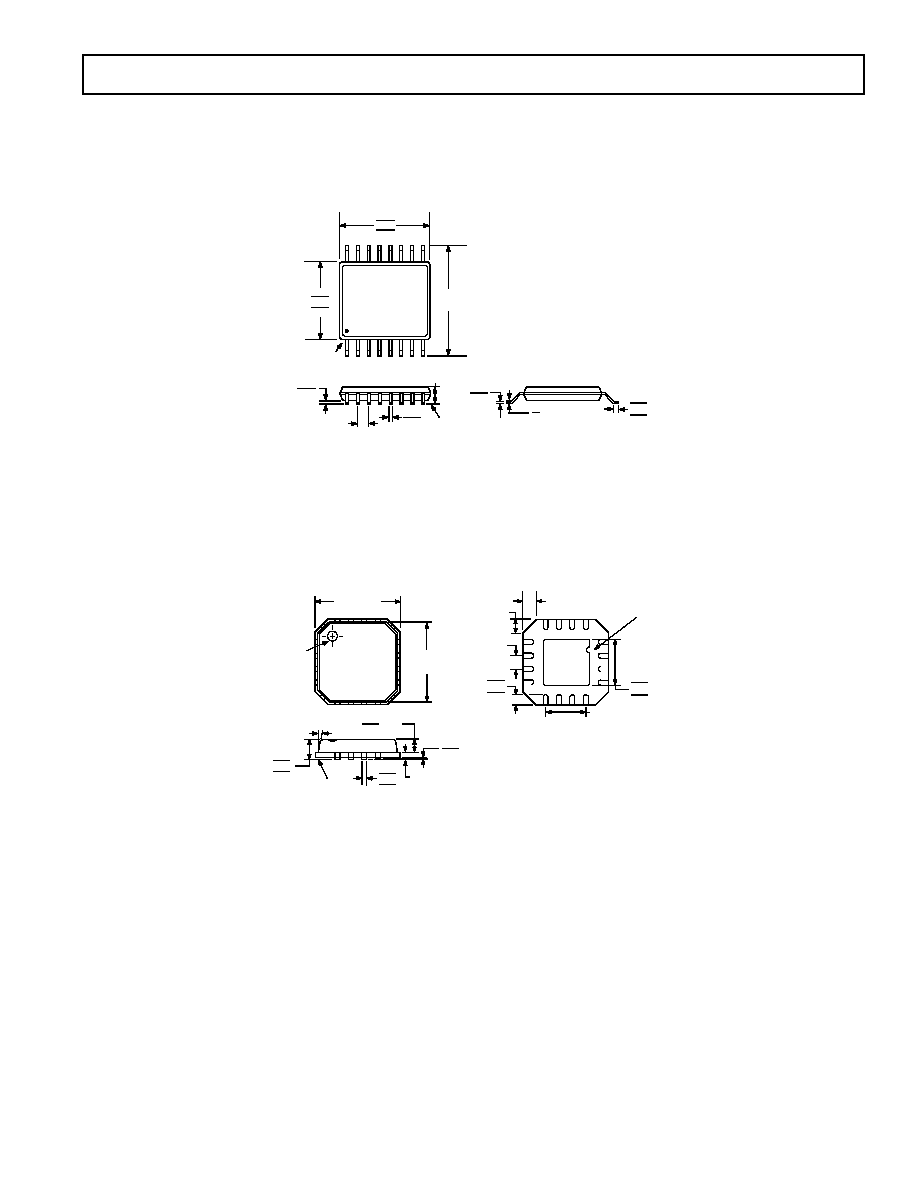
OUTLINE DIMENSIONS
16-Lead Thin Shrink Small Outline Package [TSSOP]
(RU-16)
Dimensions shown in millimeters
16
9
8
1
PIN 1
SEATING
PLANE
8
0
4.50
4.40
4.30
6.40
BSC
5.10
5.00
4.90
0.65
BSC
0.15
0.05
1.20
MAX
0.20
0.09
0.75
0.60
0.45
0.30
0.19
COPLANARITY
0.10
COMPLIANT TO JEDEC STANDARDS MO-153AB
16-Lead Lead Frame Chip Scale Package [LFCSP]
4 mm 4 mm Body
(CP-16)
Dimensions shown in millimeters
16
5
13
8
9
12
1
4
BOTTOM
VIEW
2.25
1.70
0.75
0.75
0.55
0.35
0.65 BSC
1.95 BSC
0.38
0.30
0.23
12 MAX
0.20 REF
SEATING
PLANE
PIN 1
INDICATOR
TOP
VIEW
4.0
BSC SQ
3.75
BSC SQ
0.60 MAX
0.60 MAX
0.05 MAX
0.02 NOM
1.00 MAX
0.65 NOM
COMPLIANT TO JEDEC STANDARDS MO-220-VGGC
PIN 1
INDICATOR
1.00
0.90
0.80
COPLANARITY
0.08
SQ
REV. 0

C0327302/03(0)
PRIN
TED IN U
.S.A.
12
Document Outline