 | ÐлекÑÑоннÑй компоненÑ: ADG662 | СкаÑаÑÑ:  PDF PDF  ZIP ZIP |
Äîêóìåíòàöèÿ è îïèñàíèÿ www.docs.chipfind.ru
REV. 0
Information furnished by Analog Devices is believed to be accurate and
reliable. However, no responsibility is assumed by Analog Devices for its
use, nor for any infringements of patents or other rights of third parties
which may result from its use. No license is granted by implication or
otherwise under any patent or patent rights of Analog Devices.
a
ADG661/ADG662/ADG663
One Technology Way, P.O. Box 9106, Norwood, MA 02062-9106, U.S.A.
Tel: 781/329-4700
World Wide Web Site: http://www.analog.com
Fax: 781/326-8703
© Analog Devices, Inc., 1998
LC
2
MOS
Precision 5 V Quad SPST Switches
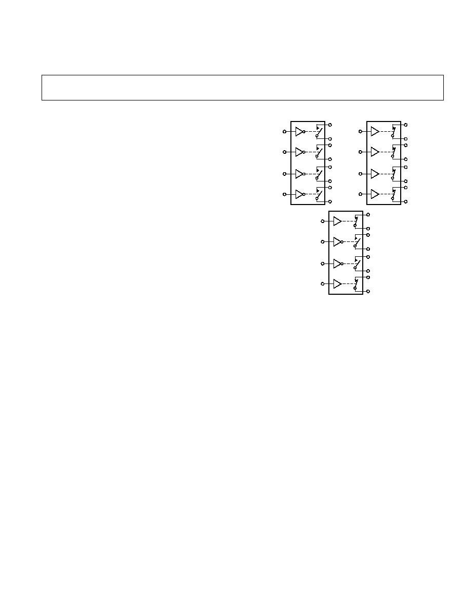
FUNCTIONAL BLOCK DIAGRAM
FEATURES
+5 V, 5 V Power Supplies
Ultralow Power Dissipation (<0.5 W)
Low Leakage (<100 pA)
Low On Resistance (<50 )
Fast Switching Times
Low Charge Injection
TTL/CMOS Compatible
TSSOP Package
APPLICATIONS
Battery Powered Instruments
Single Supply Systems
Remote Powered Equipment
+5 V Supply Systems
Computer Peripherals such as Disk Drives
Precision Instrumentation
Audio and Video Switching
Automatic Test Equipment
Precision Data Acquisition
Sample Hold Systems
Communication Systems
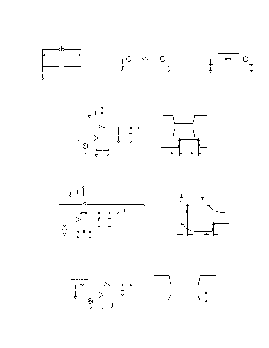
Each switch conducts equally well in both directions when ON
and has an input signal range that extends to the supplies. In the
OFF condition, signal levels up to the supplies are blocked. All
switches exhibit break-before-make switching action for use in
multiplexer applications. Inherent in the design is low charge
injection for minimum transients when switching the digital
inputs.
PRODUCT HIGHLIGHTS
1. +5 V Single Supply Operation
The ADG661, ADG662 and ADG663 offer high perfor-
mance, including low on resistance and wide signal range,
fully specified and guaranteed with
±
5 V and +5 V supply
rails.
2. Ultralow Power Dissipation
CMOS construction ensures ultralow power dissipation.
3. Low R
ON
4. Break-Before-Make Switching
This prevents channel shorting when the switches are config-
ured as a multiplexer.
GENERAL DESCRIPTION
The ADG661, ADG662 and ADG663 are monolithic CMOS
devices comprising four independently selectable switches.
These switches feature low, well-controlled on resistance and
wide analog signal range, making them ideal for precision analog
signal switching.
They are fabricated using Analog Devices' advanced linear
compatible CMOS (LC
2
MOS) process, which offers benefits of
low leakage currents, ultralow power dissipation and low capaci-
tance for fast switching speeds with minimum charge injection.
The on resistance profile is very flat over the full analog input
range ensuring excellent linearity and low distortion when
switching audio signals. Fast switching speed coupled with high
signal bandwidth also make the parts suitable for video signal
switching. CMOS construction ensures ultralow power dissipa-
tion making the parts ideally suited for portable and battery
powered instruments.
The ADG661, ADG662 and ADG663 contain four indepen-
dent SPST switches. The ADG661 and ADG662 differ only in
that the digital control logic is inverted. The ADG661 switches
are turned on with a logic low on the appropriate control input,
while a logic high is required for the ADG662. The ADG663
has two switches with digital control logic similar to that of the
ADG661, while the logic is inverted on the other two switches.
IN1
IN2
IN3
IN4
S1
D1
S2
D2
S3
D3
S4
D4
ADG661
IN1
IN2
IN3
IN4
S1
D1
S2
D2
S3
D3
S4
D4
ADG662
IN1
IN2
IN3
IN4
S1
D1
S2
D2
S3
D3
S4
D4
ADG663
SWITCHES SHOWN FOR A LOGIC "1" INPUT

2
REV. 0
ADG661/ADG662/ADG663SPECIFICATIONS
1
Dual Supply
B Versions
Parameter
+25 C
40 C to +85 C
Units
Test Conditions/Comments
ANALOG SWITCH
Analog Signal Range
V
DD
to V
SS
V
R
ON
30
typ
V
D
= 3.5 V to +3.5 V, I
S
= 10 mA;
38
50
max
V
DD
= +4.5 V, V
SS
= 4.5 V
LEAKAGE CURRENTS
V
DD
= +5.5 V, V
SS
= 5.5 V
Source OFF Leakage I
S
(OFF)
±
0.025
nA typ
V
D
=
±
4.5 V, V
S
=
±
4.5 V;
±
0.1
±
2.5
nA max
Test Circuit 2
Drain OFF Leakage I
D
(OFF)
±
0.025
nA typ
V
D
=
±
4.5 V, V
S
=
±
4.5 V;
±
0.1
±
2.5
nA max
Test Circuit 2
Channel ON Leakage I
D
, I
S
(ON)
±
0.05
nA typ
V
D
= V
S
=
±
4.5 V;
±
0.2
±
5
nA max
Test Circuit 3
DIGITAL INPUTS
Input High Voltage, V
INH
2.4
V min
Input Low Voltage, V
INL
0.8
V max
Input Current
I
INL
or I
INH
0.005
µ
A typ
V
IN
= V
INL
or V
INH
±
0.1
µ
A max
DYNAMIC CHARACTERISTICS
2
t
ON
150
ns typ
R
L
= 300
, C
L
= 35 pF;
275
ns max
V
S
=
±
3 V; Test Circuit 4
t
OFF
55
ns typ
R
L
= 300
, C
L
= 35 pF;
120
ns max
V
S
=
±
3 V; Test Circuit 4
Break-Before-Make Time Delay, t
D
80
ns typ
R
L
= 300
, C
L
= 35 pF;
(ADG663 Only)
V
S1
= V
S2
= +3 V; Test Circuit 5
Charge Injection
6
pC typ
V
S
= 0 V, R
S
= 0
, C
L
= 10 nF;
Test Circuit 6
OFF Isolation
70
dB typ
R
L
= 50
, C
L
= 5 pF, f = 1 MHz;
Test Circuit 7
Channel-to-Channel Crosstalk
90
dB typ
R
L
= 50
, C
L
= 5 pF, f = 1 MHz;
Test Circuit 8
C
S
(OFF)
9
pF typ
f = 1 MHz
C
D
(OFF)
9
pF typ
f = 1 MHz
C
D
, C
S
(ON)
28
pF typ
f = 1 MHz
POWER REQUIREMENTS
+4.5/5.5
V min/max
V
DD
4.5/5.5
V min/max
I
DD
0.0001
µ
A typ
V
DD
= +5.5 V, V
SS
= 5.5 V
1
µ
A max
Digital Inputs = 0 V or 5 V
I
SS
0.0001
µ
A typ
1
µ
A max
NOTES
1
Temperature ranges are as follows: B Versions, 40
°
C to +85
°
C.
2
Guaranteed by design, not subject to production test.
Specifications subject to change without notice.
(V
DD
= +5 V 10%, V
SS
= 5 V 10%, GND = 0 V, unless otherwise noted)

3
REV. 0
ADG661/ADG662/ADG663
Single Supply
B Versions
Parameter
+25 C
40 C to +85 C
Units
Test Conditions/Comments
ANALOG SWITCH
Analog Signal Range
0 V to V
DD
V
R
ON
45
typ
V
D
= 0 V to +3.5 V, I
S
= 10 mA;
68
75
max
V
DD
= +4.5 V
LEAKAGE CURRENTS
V
DD
= +5.5 V
Source OFF Leakage I
S
(OFF)
±
0.025
nA typ
V
D
= 4.5 V/1 V, V
S
= 1 V/4.5 V;
±
0.1
±
2.5
nA max
Test Circuit 2
Drain OFF Leakage I
D
(OFF)
±
0.025
nA typ
V
D
= 4.5 V/1 V, V
S
= 1 V/4.5 V;
±
0.1
±
2.5
nA max
Test Circuit 2
Channel ON Leakage I
D
, I
S
(ON)
±
0.05
nA typ
V
D
= V
S
= +4.5 V/+1 V;
±
0.2
±
5
nA max
Test Circuit 3
DIGITAL INPUTS
Input High Voltage, V
INH
2.4
V min
Input Low Voltage, V
INL
0.8
V max
Input Current
I
INL
or I
INH
0.005
µ
A typ
V
IN
= V
INL
or V
INH
±
0.1
µ
A max
DYNAMIC CHARACTERISTICS
2
t
ON
250
ns typ
R
L
= 300
, C
L
= 35 pF;
400
ns max
V
S
= +2 V; Test Circuit 4
t
OFF
45
ns typ
R
L
= 300
, C
L
= 35 pF;
100
ns max
V
S
= +2 V; Test Circuit 4
Break-Before-Make Time Delay, t
D
140
ns typ
R
L
= 300
, C
L
= 35 pF;
(ADG663 Only)
V
S1
= V
S2
= +2 V; Test Circuit 5
Charge Injection
12
pC typ
V
S
= 0 V, R
S
= 0
, C
L
= 10 nF;
Test Circuit 6
OFF Isolation
70
dB typ
R
L
= 50
, C
L
= 5 pF, f = 1 MHz;
Test Circuit 7
Channel-to-Channel Crosstalk
90
dB typ
R
L
= 50
, C
L
= 5 pF, f = 1 MHz;
Test Circuit 8
C
S
(OFF)
9
pF typ
f = 1 MHz
C
D
(OFF)
9
pF typ
f = 1 MHz
C
D
, C
S
(ON)
28
pF typ
f = 1 MHz
POWER REQUIREMENTS
V
DD
+4.5/5.5
V min/max
I
DD
0.0001
µ
A typ
V
DD
= +5.5 V
1
µ
A max
Digital Inputs = 0 V or 5 V
NOTES
1
Temperature ranges are as follows: B Versions, 40
°
C to +85
°
C.
2
Guaranteed by design, not subject to production test.
Specifications subject to change without notice.
(V
DD
= +5 V 10%, V
SS
= 0 V, GND = 0 V, unless otherwise noted)
ADG661/ADG662/ADG663
4
REV. 0
CAUTION
ESD (electrostatic discharge) sensitive device. Electrostatic charges as high as 4000 V readily
accumulate on the human body and test equipment and can discharge without detection.
Although the ADG661/ADG662/ADG663 features proprietary ESD protection circuitry, per-
manent damage may occur on devices subjected to high energy electrostatic discharges. There-
fore, proper ESD precautions are recommended to avoid performance degradation or loss of
functionality.
WARNING!
ESD SENSITIVE DEVICE
ORDERING GUIDE
Temperature
Package
Package
Model
Range
Description
Option
ADG661BRU
40
°
C to +85
°
C
16-Lead TSSOP
RU-16
ADG662BRU
40
°
C to +85
°
C
16-Lead TSSOP
RU-16
ADG663BRU
40
°
C to +85
°
C
16-Lead TSSOP
RU-16
ABSOLUTE MAXIMUM RATINGS
1
(T
A
= +25
°
C unless otherwise noted)
V
DD
to V
SS
. . . . . . . . . . . . . . . . . . . . . . . . . . . . . . . . . . . . +44 V
V
DD
to GND . . . . . . . . . . . . . . . . . . . . . . . . . . 0.3 V to +25 V
V
SS
to GND . . . . . . . . . . . . . . . . . . . . . . . . . . . +0.3 V to 25 V
Analog, Digital Inputs
2
. . . . . . . . . . . V
SS
2 V to V
DD
+2 V or
30 mA, Whichever Occurs First
Continuous Current, S or D . . . . . . . . . . . . . . . . . . . . . 30 mA
Peak Current, S or D . . . . . . . . . . . . . . . . . . . . . . . . . . 100 mA
(Pulsed at 1 ms, 10% Duty Cycle max)
Operating Temperature Range
Industrial (B Version) . . . . . . . . . . . . . . . . . 40
°
C to +85
°
C
Storage Temperature Range . . . . . . . . . . . . . 65
°
C to +150
°
C
Junction Temperature . . . . . . . . . . . . . . . . . . . . . . . . . +150
°
C
TSSOP Package, Power Dissipation . . . . . . . . . . . . . . 450 mW
JA
Thermal Impedance . . . . . . . . . . . . . . . . . . . . . . . 115
°
C/W
JC
Thermal Impedance . . . . . . . . . . . . . . . . . . . . . . . . 35
°
C/W
Lead Temperature, Soldering
Vapor Phase (60 secs) . . . . . . . . . . . . . . . . . . . . . . . +215
°
C
Infrared (15 secs) . . . . . . . . . . . . . . . . . . . . . . . . . . . +220
°
C
NOTES
1
Stresses above those listed under Absolute Maximum Ratings may cause perma-
nent damage to the device. This is a stress rating only; functional operation of the
device at these or any other conditions above those listed in the operational
sections of this specification is not implied. Exposure to absolute maximum rating
conditions for extended periods may affect device reliability. Only one absolute
maximum rating may be applied at any one time.
2
Overvoltages at IN, S or D will be clamped by internal diodes. Current should be
limited to the maximum ratings given.
ADG661/ADG662/ADG663
5
REV. 0
TERMINOLOGY
V
DD
Most positive power supply potential.
V
SS
Most negative power supply potential in
dual supplies. In single supply applications,
it may be connected to GND.
GND
Ground (0 V) Reference.
S
Source Terminal. May be an input or output.
D
Drain Terminal. May be an input or output.
IN
Logic Control Input.
R
ON
Ohmic resistance between D and S.
I
S
(OFF)
Source leakage current with the switch "OFF."
I
D
(OFF)
Drain leakage current with the switch "OFF."
I
D
, I
S
(ON)
Channel leakage current with the switch "ON."
V
D
(V
S
)
Analog voltage on terminals D, S.
C
S
(OFF)
"OFF" Switch Source Capacitance.
C
D
(OFF)
"OFF" Switch Drain Capacitance.
C
D
, C
S
(ON)
"ON" Switch Capacitance.
t
ON
Delay between applying the digital control
input and the output switching on.
t
OFF
Delay between applying the digital control
input and the output switching off.
t
D
"OFF" time or "ON" time measured between
the 90% points of both switches, when
switching from one address state to another.
Crosstalk
A measure of unwanted signal which is
coupled through from one channel to another
as a result of parasitic capacitance.
Off Isolation
A measure of unwanted signal coupling
through an "OFF" switch.
Charge
A measure of the glitch impulse transferred
Injection
from the digital input to analog output during
switching.
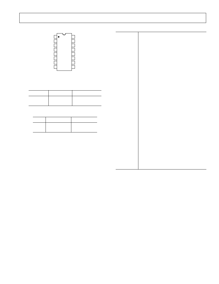
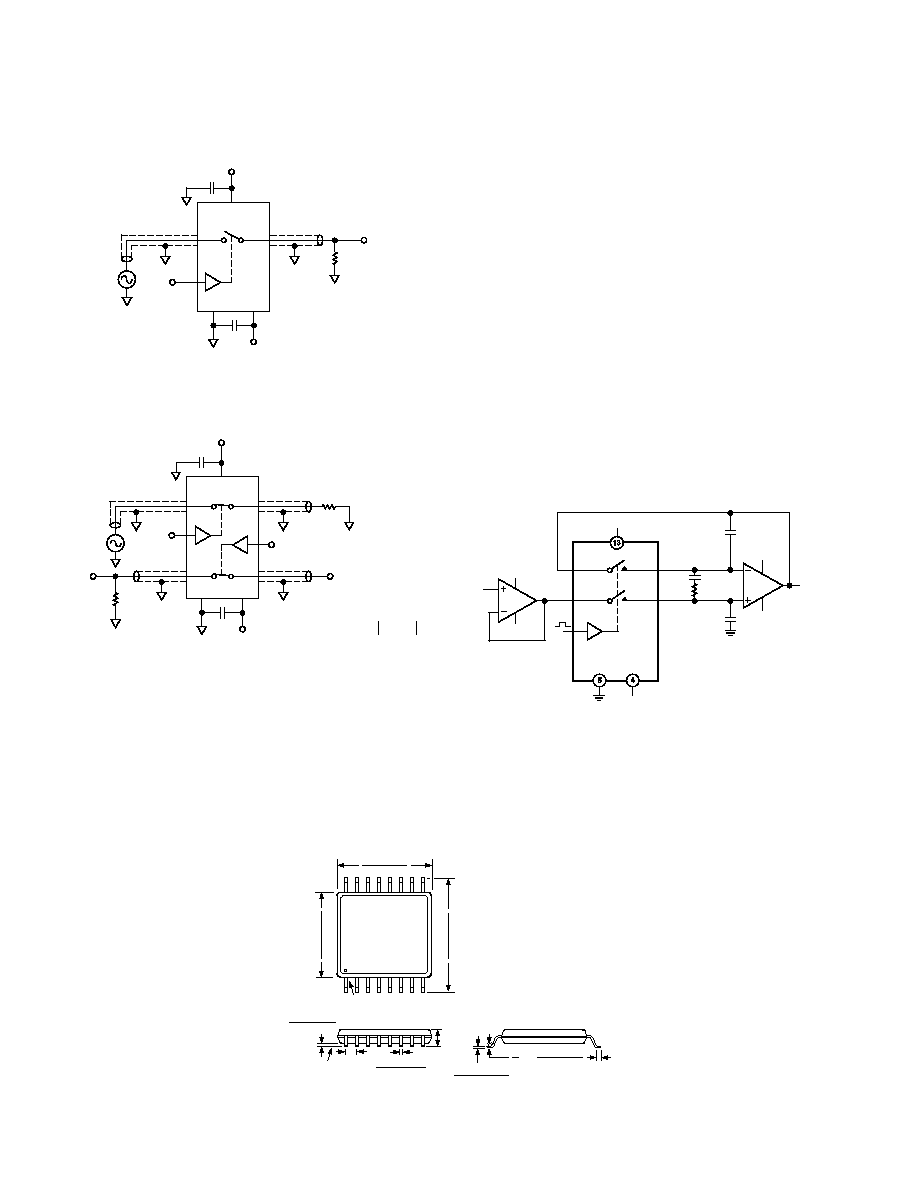
PIN CONFIGURATION
Table I. Truth Table (ADG661/ADG662)
ADG661 In
ADG662 In
Switch Condition
0
1
ON
1
0
OFF
Table II. Truth Table (ADG663)
Logic
Switch 1, 4
Switch 2, 3
0
OFF
ON
1
ON
OFF
TOP VIEW
(Not to Scale)
16
15
14
13
12
11
10
9
1
2
3
4
5
6
7
8
IN1
D1
S1
V
SS
GND
S4
D4
IN4
IN2
D2
S2
V
DD
NC
S3
D3
IN3
ADG661
ADG662
ADG663
NC
=
NO
CONNECT
ADG661/ADG662/ADG663
6
REV. 0
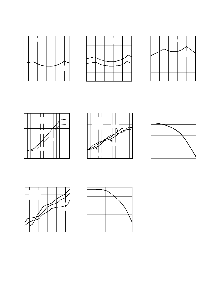
Typical Performance Characteristics
50
0
30
10
20
40
V
D
OR V
S
DRAIN OR SOURCE VOLTAGE V
5
5
4
3
4
2
1
0
1
2
3
T
A
= +25 C
V
DD
= +5V
V
SS
= 5V
R
ON
Figure 1. On Resistance as a
Function of V
D
(V
S
) Dual Supplies
10nA
100nA
1 A
10 A
100 A
100k
10M
100
1k
10k
1M
FREQUENCY Hz
10
1mA
10mA
I
SUPPLY
4 SW
1 SW
I, I+
V
DD
= +5V
V
SS
= 5V
Figure 4. Supply Current vs. Input
Switching Frequency
V
D
OR V
S
DRAIN OR SOURCE VOLTAGE
0.006
0.000
0.006
5
5
4
3
2
1
0
1
2
3
4
0.004
0.002
0.002
0.004
V
DD
= +5V
V
SS
= 5V
T
A
= +25 C
I
D
(OFF)
I
S
(OFF)
I
D
(ON)
LEAKAGE CURRENT nA
Figure 7. Leakage Currents as a
Function of V
D
(V
S
)
50
0
30
10
20
40
V
D
OR V
S
DRAIN OR SOURCE VOLTAGE V
5
5
4
3
4
2
1
0
1
2
3
V
DD
= +5V
V
SS
= 5V
+85 C
+25 C
R
ON
Figure 2. On Resistance as a
Function of V
D
(V
S
) for
Different Temperatures
10
0.001
25
1
0.01
35
0.1
105
95
85
75
65
55
45
TEMPERATURE C
I
D
(OFF)
I
D
(ON)
I
S
(OFF)
V
DD
= +5V
V
SS
= 5V
V
S
= 5V
V
D
= 5V
LEAKAGE CURRENT nA
Figure 5. Leakage Currents as a
Function of Temperature
FREQUENCY Hz
110
100
60
100
10M
1k
10k
100k
1M
90
80
70
V
DD
= +5V
V
SS
= 5V
CROSSTALK dB
Figure 8. Crosstalk vs. Frequency
V
D
OR V
S
DRAIN OR SOURCE VOLTAGE V
R
ON
50
0
0
1
5
2
3
4
40
30
20
10
T
A
= +25°C
V
DD
= +5V
V
SS
= 0V
Figure 3. On Resistance as a
Function of V
D
(V
S
) Single Supply
40
FREQUENCY Hz
120
100
100
10M
1k
10k
100k
1M
80
60
V
DD
= +5V
V
SS
= 5V
OFF ISOLATION dB
Figure 6. Off Isolation vs.
Frequency
ADG661/ADG662/ADG663
7
REV. 0
1. On Resistance
2. Off Leakage
I
DS
V1
S
D
V
S
R
ON
= V1/I
DS
S
D
V
S
A
V
D
A
I
S
(OFF)
I
D
(OFF)
S
D
V
S
V
D
A
I
D
(ON)
4. Switching Times
3. On Leakage
S1
D1
0.1 F
V
DD
IN1, IN2
V
S1
GND
V
SS
R
L1
300
C
L1
35pF
V
OUT1
0.1 F
V
S2
V
OUT2
R
L2
300
C
L2
35pF
S2
V
IN
D2
V
DD
V
SS
t
D
t
D
3V
50%
50%
90%
V
IN
V
OUT1
V
OUT2
90%
90%
90%
0V
0V
0V
5. Break-Before-Make Time Delay
S
D
V
DD
IN
V
S
GND
V
SS
C
L
10nF
V
OUT
R
S
V
SS
V
DD
3V
V
IN
V
OUT
V
OUT
Q
INJ
= C
L
V
OUT
6. Charge Injection
S
D
V
DD
0.1 F
V
DD
IN
V
S
GND
V
SS
R
L
300
C
L
35pF
V
OUT
0.1 F
V
SS
t
ON
t
OFF
3V
50%
50%
50%
50%
3V
90%
90%
V
IN
V
IN
V
OUT
ADG661
ADG662
Test Circuits
8
REV. 0
C325781/98
PRINTED IN U.S.A.
ADG661/ADG662/ADG663
S
D
0.1 F
V
DD
IN
V
S
GND
V
SS
R
L
50
V
OUT
0.1 F
V
IN
V
SS
V
DD
7. Off Isolation
16-Lead TSSOP
(RU-16)
16
9
8
1
0.201 (5.10)
0.193 (4.90)
0.256 (6.50)
0.246 (6.25)
0.177 (4.50)
0.169 (4.30)
PIN 1
SEATING
PLANE
0.006 (0.15)
0.002 (0.05)
0.0118 (0.30)
0.0075 (0.19)
0.0256
(0.65)
BSC
0.0433
(1.10)
MAX
0.0079 (0.20)
0.0035 (0.090)
0.028 (0.70)
0.020 (0.50)
8°
0°
OUTLINE DIMENSIONS
Dimensions shown in inches and (mm).
Test Circuits (Continued)
8. Channel-to-Channel Crosstalk
S
D
0.1 F
V
DD
V
S
GND
V
SS
50
NC
0.1 F
V
IN1
V
IN2
S
D
R
L
50
V
OUT
CHANNEL TO CHANNEL
CROSSTALK = 20 LOG V
S
/V
OUT
V
DD
V
SS
APPLICATION
Figure 9 illustrates a precise, sample-and-hold circuit. An
AD845 is used as the input buffer while the output operational
amplifier is an OP07. During the track mode, SW1 is closed and
the output V
OUT
follows the input signal V
IN
. In the hold mode,
SW1 is opened and the signal is held by the hold capacitor C
H
.
Due to switch and capacitor leakage, the voltage on the hold
capacitor will decrease with time. The ADG661/ADG662/
ADG663 minimizes this droop due to its low leakage specifica-
tions. The droop rate is further minimized by the use of a poly-
styrene hold capacitor. The droop rate for the circuit shown is
typically 15
µ
V/
µ
s.
A second switch SW2, which operates in parallel with SW1, is
included in this circuit to reduce pedestal error. Since both
switches will be at the same potential, they will have a differen-
tial effect on the op amp OP07 which will minimize charge
injection effects. Pedestal error is also reduced by the compensa-
tion network R
C
and C
C
. This compensation network also re-
duces the hold time glitch while optimizing the acquisition time.
Using the illustrated op amps and component values, the pedes-
tal error has a maximum value of 5 mV over the
±
3 V input
range. The acquisition time is 2.5 ms while the settling time is
1.85
µ
s.
+5V
5V
2200pF
R
C
75
C
C
1000pF
C
H
2200pF
V
OUT
ADG661
ADG662
ADG663
SW2
SW1
S
S
D
D
+5V
5V
AD845
+5V
5V
V
IN
OP07
Figure 9. Accurate Sample-and-Hold