 | ÐлекÑÑоннÑй компоненÑ: ADG714 | СкаÑаÑÑ:  PDF PDF  ZIP ZIP |
Äîêóìåíòàöèÿ è îïèñàíèÿ www.docs.chipfind.ru
REV. 0
Information furnished by Analog Devices is believed to be accurate and
reliable. However, no responsibility is assumed by Analog Devices for its
use, nor for any infringements of patents or other rights of third parties
which may result from its use. No license is granted by implication or
otherwise under any patent or patent rights of Analog Devices.
a
ADG714/ADG715
One Technology Way, P.O. Box 9106, Norwood, MA 02062-9106, U.S.A.
Tel: 781/329-4700
World Wide Web Site: http://www.analog.com
Fax: 781/326-8703
© Analog Devices, Inc., 2000
CMOS, Low Voltage
Serially-Controlled, Octal SPST Switches
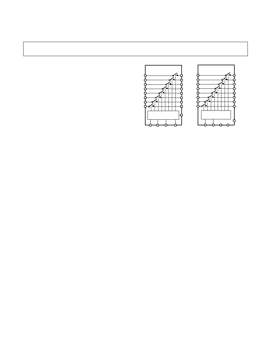
FUNCTIONAL BLOCK DIAGRAMS
ADG714
D1
D2
D3
D4
D5
D6
D7
D8
DOUT
S1
S2
S3
S4
S5
S6
S7
S8
INPUT SHIFT
REGISTER
SCLK DIN
SYNC RESET
ADG715
D1
D2
D3
D4
D5
D6
D7
D8
S1
S2
S3
S4
S5
S6
S7
S8
INTERFACE
LOGIC
SDA SCL A0 A1
RESET
FEATURES
ADG714 SPITM/QSPITM/MICROWIRETM-Compatible Interface
ADG715 I
2
CTM-Compatible Interface
2.7 V to 5.5 V Single Supply
3 V Dual Supply
2.5
On Resistance
0.6
On Resistance Flatness
100 pA Leakage Currents
Octal SPST
Power-On Reset
Fast Switching Times
TTL/CMOS-Compatible
Small TSSOP Package
APPLICATIONS
Data Acquisition Systems
Communication Systems
Relay Replacement
Audio and Video Switching
GENERAL DESCRIPTION
The ADG714/ADG715 are CMOS, octal SPST (single-pole,
single-throw) switches controlled via either a two- or 3-wire
serial interface. On resistance is closely matched between switches
and very flat over the full signal range. Each switch conducts
equally well in both directions and the input signal range extends
to the supplies. Data is written to these devices in the form of
8 bits, each bit corresponding to one channel.
The ADG714 utilizes a 3-wire serial interface that is compatible
with SPI
, QSPI
and MICROWIRE
and most DSP interface
standards. The output of the shift register DOUT enables a
number of these parts to be daisy chained.
The ADG715 utilizes a 2-wire serial interface that is compatible
with the I
2
C interface standard. The ADG715 has four hard wired
addresses, selectable from two external address pins (A0 and A1).
This allows the 2 LSBs of the 7-bit slave address to be set by the
user. A maximum of four of these devices may be connected to
the bus.
On power-up of these devices, all switches are in the OFF con-
dition, and the internal registers contain all zeros.
Low power consumption and operating supply range of 2.7 V to
5.5 V make this part ideal for many applications. These parts
may also be supplied from a dual
± 3 V supply. The ADG714
and ADG715 are available in a small 24-lead TSSOP package.
PRODUCT HIGHLIGHTS
1. 2-3-Wire Serial Interface.
2. Single/Dual Supply Operation. The ADG714 and ADG715
are fully specified and guaranteed with 3 V, 5 V, and
±3 V
supply rails.
3. Low On Resistance, typically 2.5
.
4. Low Leakage.
5. Power-On Reset.
6. Small 24-lead TSSOP package.
I
2
C is a trademark of Philips Corporation.
SPI and QSPI are trademarks of Motorola, Inc.
MICROWIRE is a trademark of National Semiconductor Corporation.
2
REV. 0
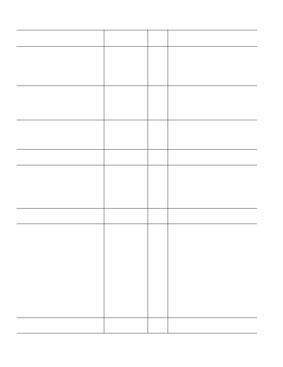
ADG714/ADG715SPECIFICATIONS
(V
DD
= 5 V 10%, V
SS
= 0 V, GND = 0 V unless otherwise noted)
B Version
40 C
Parameter
+25 C
to +85 C
Unit
Test Conditions/Comments
ANALOG SWITCH
Analog Signal Range
0 V to V
DD
V
On Resistance (R
ON
)
2.5
typ
V
S
= 0 V to V
DD
, I
S
= 10 mA
4.5
5
max
On-Resistance Match Between Channels (
R
ON
)
0.4
typ
0.8
max
V
S
= 0 V to V
DD
, I
S
= 10 mA
On-Resistance Flatness (R
FLAT(ON)
)
0.6
typ
V
S
= 0 V to V
DD
, I
S
= 10 mA
1.2
max
LEAKAGE CURRENTS
V
DD
= 5.5 V
Source OFF Leakage I
S
(OFF)
±0.01
nA typ
V
D
= 4.5 V/1 V, V
S
= 1 V/4.5 V
±0.1
±0.3
nA max
Drain OFF Leakage I
D
(OFF)
±0.01
nA typ
V
D
= 4.5 V/1 V, V
S
= 1 V/4.5 V
±0.1
±0.3
nA max
Channel ON Leakage I
D
, I
S
(ON)
±0.01
nA typ
V
D
= V
S
= 1 V, or 4.5 V
±0.1
±0.3
nA max
DIGITAL INPUTS (SCLK, DIN,
SYNC, A0, A1)
Input High Voltage, V
INH
2.4
V min
Input Low Voltage, V
INL
0.8
V max
Input Current, I
INL
or I
INH
0.005
µA typ
V
IN
= V
INL
or V
INH
±0.1
µA max
C
IN
, Digital Input Capacitance
2
3
pF typ
DIGITAL OUTPUT ADG714 DOUT
2
Output Low Voltage
0.4
max
I
SINK
= 6 mA
C
OUT
Digital Output Capacitance
4
pF typ
DIGITAL INPUTS (SCL, SDA)
2
Input High Voltage, V
INH
0.7 V
DD
V min
V
DD
+ 0.3
V max
Input Low Voltage, V
INL
0.3
V min
0.3 V
DD
V max
I
IN
, Input Leakage Current
0.005
µA typ
V
IN
= 0 V to V
DD
± 1
µA max
V
HYST
, Input Hysteresis
0.05 V
DD
V min
C
IN
, Input Capacitance
6
pF typ
LOGIC OUTPUT (SDA)
2
V
OL
, Output Low Voltage
0.4
V max
I
SINK
= 3 mA
0.6
V max
I
SINK
= 6 mA
DYNAMIC CHARACTERISTICS
2
t
ON
ADG714
20
ns typ
V
S
= 3 V, R
L
= 300
, C
L
= 35 pF
32
ns max
t
ON
ADG715
95
ns typ
V
S
= 3 V, R
L
= 300
, C
L
= 35 pF
140
ns max
t
OFF
ADG714
8
ns typ
V
S
= 3 V, R
L
= 300
, C
L
= 35 pF
15
ns max
t
OFF
ADG715
85
ns typ
V
S
= 3 V, R
L
= 300
, C
L
= 35 pF
130
ns max
Break-Before-Make Time Delay, t
D
8
ns typ
V
S
= 3 V, R
L
= 300
, C
L
= 35 pF
1
ns min
Charge Injection
± 3
pC typ
V
S
= 2 V, R
S
= 0
, C
L
= 1 nF
Off Isolation
60
dB typ
R
L
= 50
, C
L
= 5 pF, f = 10 MHz
80
dB typ
R
L
= 50
, C
L
= 5 pF, f = 1 MHz
Channel-to-Channel Crosstalk
70
dB typ
R
L
= 50
, C
L
= 5 pF, f = 10 MHz
90
dB typ
R
L
= 50
, C
L
= 5 pF, f = 1 MHz
3 dB Bandwidth
155
MHz typ
R
L
= 50
, C
L
= 5 pF
C
S
(OFF)
11
pF typ
C
D
(OFF)
11
pF typ
C
D
, C
S
(ON)
22
pF typ
POWER REQUIREMENTS
V
DD
= 5.5 V
I
DD
10
µA typ
Digital Inputs = 0 V or 5.5 V
20
µA max
NOTES
1
Temperature range is as follows: B Version: 40
°C to +85°C.
2
Guaranteed by design, not subject to production test.
Specifications subject to change without notice.
1
3
REV. 0
ADG714/ADG715
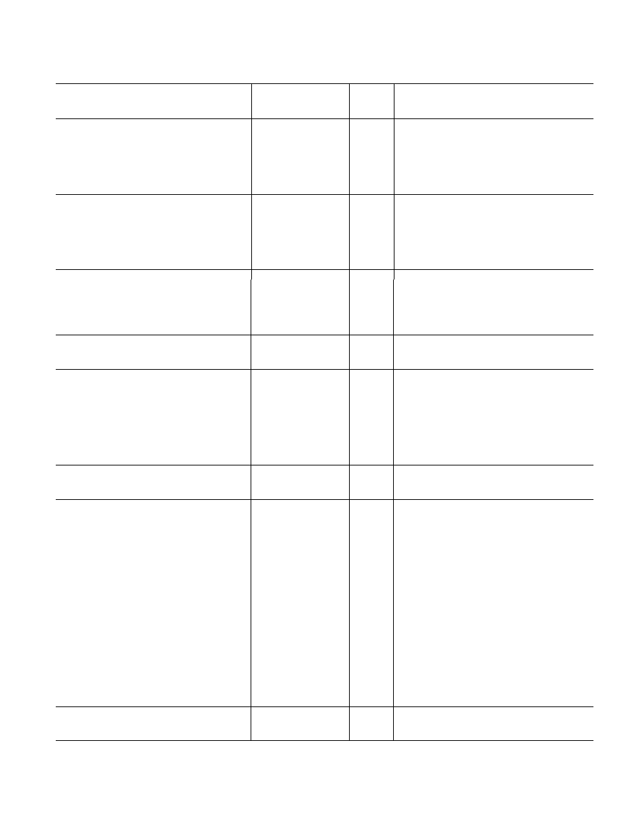
SPECIFICATIONS
1
(V
DD
= 3 V 10%, V
SS
= 0 V, GND = 0 V unless otherwise noted)
B Version
40 C
Parameter
+25 C
to +85 C
Unit
Test Conditions/Comments
ANALOG SWITCH
Analog Signal Range
0 V to V
DD
V
On Resistance (R
ON
)
6
typ
V
S
= 0 V to V
DD
, I
S
= 10 mA
11
12
max
On-Resistance Match Between Channels (
R
ON
)
0.4
typ
V
S
= 0 V to V
DD
, I
S
= 10 mA
1.2
max
On-Resistance Flatness (R
FLAT(ON)
)
3.5
typ
V
S
= 0 V to V
DD
, I
S
= 10 mA
LEAKAGE CURRENTS
V
DD
= 3.3 V
Source OFF Leakage I
S
(OFF)
±0.01
nA typ
V
S
= 3 V/1 V, V
D
= 1 V/3 V
±0.1
±0.3
nA max
Drain OFF Leakage I
D
(OFF)
±0.01
nA typ
V
S
= 1 V/3 V, V
D
= 3 V/1 V
±0.1
±0.3
nA max
Channel ON Leakage I
D
, I
S
(ON)
±0.01
nA typ
V
S
= V
D
= 1 V, or 3 V
±0.1
±0.3
nA max
DIGITAL INPUTS (SCLK, DIN,
SYNC, A0, A1)
Input High Voltage, V
INH
2.0
V min
Input Low Voltage, V
INL
0.4
V max
Input Current, I
INL
or I
INH
0.005
µA typ
V
IN
= V
INL
or V
INH
±0.1
µA max
C
IN
, Digital Input Capacitance
2
3
pF typ
DIGITAL OUTPUT ADG714 DOUT
2
Output Low Voltage
0.4
max
I
SINK
= 6 mA
C
OUT
Digital Output Capacitance
4
pF typ
DIGITAL INPUTS (SCL, SDA)
2
Input High Voltage, V
INH
0.7 V
DD
V min
V
DD
+ 0.3
V max
Input Low Voltage, V
INL
0.3
V min
0.3 V
DD
V max
I
IN
, Input Leakage Current
0.005
µA typ
V
IN
= 0 V to V
DD
± 1
µA max
V
HYST
, Input Hysteresis
0.05 V
DD
V min
C
IN
, Input Capacitance
6
pF typ
LOGIC OUTPUT (SDA)
2
V
OL
, Output Low Voltage
0.4
V max
I
SINK
= 3 mA
0.6
V max
I
SINK
= 6 mA
DYNAMIC CHARACTERISTICS
2
t
ON
ADG714
35
ns typ
V
S
= 2 V, R
L
= 300
, C
L
= 35 pF
65
ns max
t
ON
ADG715
130
ns typ
V
S
= 2 V, R
L
= 300
, C
L
= 35 pF
200
ns max
t
OFF
ADG714
11
ns typ
V
S
= 2 V, R
L
= 300
, C
L
= 35 pF
20
ns max
t
OFF
ADG715
115
ns typ
V
S
= 2 V, R
L
= 300
, C
L
= 35 pF
180
ns max
Break-Before-Make Time Delay, t
D
8
ns typ
V
S
= 2 V, R
L
= 300
, C
L
= 35 pF
1
ns min
Charge Injection
± 2
pC typ
V
S
= 1.5 V, R
S
= 0
, C
L
= 1 nF
Off Isolation
60
dB typ
R
L
= 50
, C
L
= 5 pF, f = 10 MHz
80
dB typ
R
L
= 50
, C
L
= 5 pF, f = 1 MHz
Channel-to-Channel Crosstalk
70
dB typ
R
L
= 50
, C
L
= 5 pF, f = 10 MHz
90
dB typ
R
L
= 50
, C
L
= 5 pF, f = 1 MHz
3 dB Bandwidth
155
MHz typ
R
L
= 50
, C
L
= 5 pF
C
S
(OFF)
11
pF typ
C
D
(OFF)
11
pF typ
C
D
, C
S
(ON)
22
pF typ
POWER REQUIREMENTS
V
DD
= 3.3 V
I
DD
10
µA typ
Digital Inputs = 0 V or 3.3 V
20
µA max
NOTES
1
Temperature range is as follows: B Version: 40
°C to +85°C.
2
Guaranteed by design, not subject to production test.
Specifications subject to change without notice.
4
REV. 0
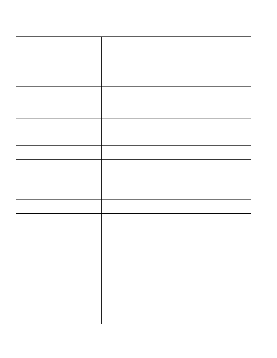
ADG714/ADG715SPECIFICATIONS
DUAL SUPPLY
1
B Version
40 C
Parameter
+25 C
to +85 C
Unit
Test Conditions/Comments
ANALOG SWITCH
Analog Signal Range
V
SS
to V
DD
V
On Resistance (R
ON
)
2.5
typ
V
S
= V
SS
to V
DD
, I
DS
= 10 mA
4.5
5
max
On-Resistance Match Between Channels (
R
ON
)
0.4
typ
V
S
= V
SS
to V
DD
, I
DS
= 10 mA
0.8
max
On-Resistance Flatness (R
FLAT(ON)
)
0.6
typ
V
S
= V
SS
to V
DD
, I
DS
= 10 mA
1
max
LEAKAGE CURRENTS
V
DD
= +3.3 V, V
SS
= 3.3 V
Source OFF Leakage I
S
(OFF)
±0.01
nA typ
V
S
= +2.25 V/1.25 V, V
D
= 1.25 V/+2.25 V
±0.1
±0.3
nA max
Drain OFF Leakage I
D
(OFF)
±0.01
nA typ
V
S
= +2.25 V/1.25 V, V
D
= 1.25 V/+2.25 V
±0.1
±0.3
nA max
Channel ON Leakage I
D
, I
S
(ON)
±0.01
nA typ
V
S
= V
D
= +2.25 V/1.25 V
±0.1
±0.3
nA max
DIGITAL INPUTS
Input High Voltage, V
INH
2.0
V min
Input Low Voltage, V
INL
0.4
V max
Input Current, I
INL
or I
INH
0.005
µA typ
V
IN
= V
INL
or V
INH
±0.1
µA max
C
IN
, Digital Input Capacitance
2
3
pF typ
DIGITAL OUTPUT ADG714 DOUT
2
Output Low Voltage
0.4
max
I
SINK
= 6 mA
C
OUT
Digital Output Capacitance
4
pF typ
DIGITAL INPUTS (SCL, SDA)
2
Input High Voltage, V
INH
0.7 V
DD
V min
V
DD
+ 0.3
V max
Input Low Voltage, V
INL
0.3
V min
0.3 V
DD
V max
I
IN
, Input Leakage Current
0.005
µA typ
V
IN
= 0 V to V
DD
±1
µA max
V
HYST
, Input Hysteresis
0.05 V
DD
V min
C
IN
, Input Capacitance
6
pF typ
LOGIC OUTPUT (SDA)
2
V
OL
, Output Low Voltage
0.4
V max
I
SINK
= 3 mA
0.6
V max
I
SINK
= 6 mA
DYNAMIC CHARACTERISTICS
2
t
ON
ADG714
20
ns typ
V
S
= 1.5 V, R
L
= 300
, C
L
= 35 pF
32
ns max
t
ON
ADG715
133
ns typ
V
S
= 1.5 V, R
L
= 300
, C
L
= 35 pF
200
ns max
t
OFF
ADG714
8
ns typ
V
S
= 1.5 V, R
L
= 300
, C
L
= 35 pF
18
ns max
t
OFF
ADG715
124
ns typ
V
S
= 1.5 V, R
L
= 300
, C
L
= 35 pF
190
ns max
Break-Before-Make Time Delay, t
D
8
ns typ
V
S
= 1.5 V, R
L
= 300
, C
L
= 35 pF
1
ns min
Charge Injection
±3
pC typ
V
S
= 0 V, R
S
= 0
, C
L
= 1 nF
Off Isolation
60
dB typ
R
L
= 50
, C
L
= 5 pF, f = 10 MHz
80
dB typ
R
L
= 50
, C
L
= 5 pF, f = 1 MHz
Channel-to-Channel Crosstalk
70
dB typ
R
L
= 50
, C
L
= 5 pF, f = 10 MHz
90
dB typ
R
L
= 50
, C
L
= 5 pF, f = 1 MHz
3 dB Bandwidth
155
MHz typ
R
L
= 50
, C
L
= 5 pF
C
S
(OFF)
11
pF typ
C
D
(OFF)
11
pF typ
C
D
, C
S
(ON)
22
pF typ
POWER REQUIREMENTS
V
DD
= +3.3 V, V
SS
= 3.3 V
I
DD
15
µA typ
Digital Inputs = 0 V or 3.3 V
25
µA max
I
SS
15
µA typ
25
µA max
NOTES
1
Temperature range is as follows: B Version: 40
°C to +85°C.
2
Guaranteed by design, not subject to production test.
Specifications subject to change without notice.
(V
DD
= +3 V 10%, V
SS
= 3 V GND = 0 V unless otherwise noted)
ADG714/ADG715
5
REV. 0
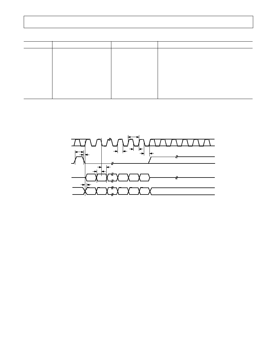
ADG714 TIMING CHARACTERISTICS
1, 2
Parameter
Limit at T
MIN
, T
MAX
Unit
Conditions/Comments
f
SCLK
30
MHz max
SCLK Cycle Frequency
t
1
33
ns min
SCLK Cycle Time
t
2
13
ns min
SCLK High Time
t
3
13
ns min
SCLK Low Time
t
4
0
ns min
SYNC to SCLK Rising Edge Setup Time
t
5
5
ns min
Data Setup Time
t
6
4.5
ns min
Data Hold Time
t
7
0
ns min
SCLK Falling Edge to
SYNC Rising Edge
t
8
33
ns min
Minimum
SYNC High Time
t
9
3
20
ns min
SCLK Rising Edge to DOUT Valid
NOTES
1
See Figure 1.
2
All input signals are specified with tr = tf = 5 ns (10% to 90% of V
DD
) and timed from a voltage level of (V
IL
+ V
IH
)/2.
3
C
L
= 20 pF, R
L
= 1 k
.
Specifications subject to change without notice.
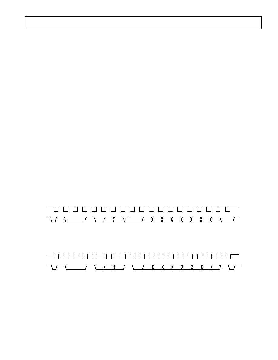
SCLK
SYNC
DIN
DOUT
t
8
t
4
t
6
t
5
t
2
t
3
t
1
t
7
t
9
DB0
DB7
DB7
1
DB6
1
DB2
1
DB1
1
DB0
1
NOTE
1
DATA FROM PREVIOUS WRITE CYCLE
Figure 1. 3-Wire Serial Interface Timing Diagram
(V
DD
= 2.7 V to 5.5 V. All specifications 40 C to +85 C unless otherwise noted.)
ADG714/ADG715
6
REV. 0
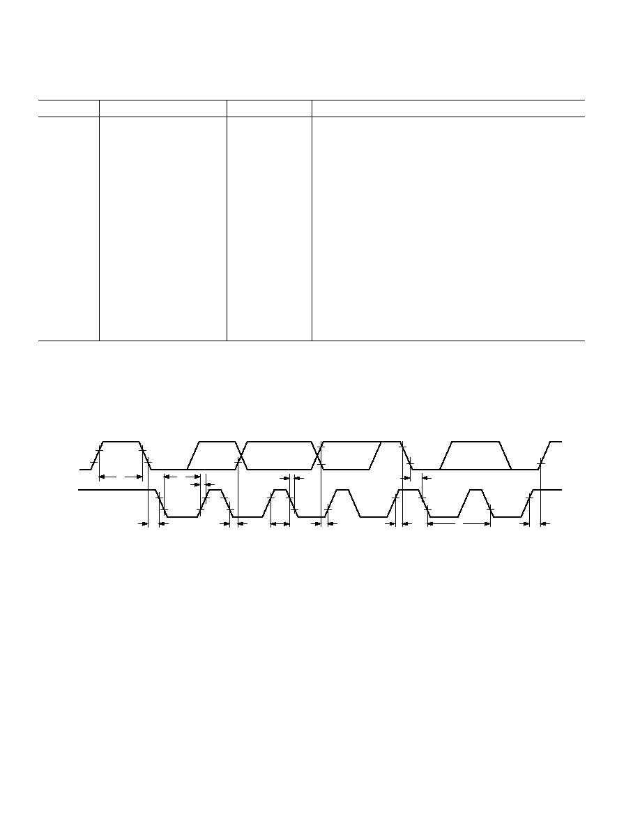
ADG715 TIMING CHARACTERISTICS
1
Parameter
Limit at T
MIN
, T
MAX
Unit
Conditions/Comments
f
SCL
400
kHz max
SCL Clock Frequency
t
1
2.5
µs min
SCL Cycle Time
t
2
0.6
µs min
t
HIGH
, SCL High Time
t
3
1.3
µs min
t
LOW
, SCL Low Time
t
4
0.6
µs min
t
HD, STA
, Start/Repeated Start Condition Hold Time
t
5
100
ns min
t
SU, DAT
, Data Setup Time
t
6
2
0.9
µs max
t
HD, DAT
, Data Hold Time
0
µs min
t
7
0.6
µs min
t
SU, STA
, Setup Time for Repeated Start
t
8
0.6
µs min
t
SU, STO
, Stop Condition Setup Time
t
9
1.3
µs min
t
BUF
, Bus Free Time Between a STOP Condition and
a Start Condition
t
10
300
ns max
t
R
, Rise Time of both SCL and SDA when Receiving
20 + 0.1C
b
3
ns min
t
11
250
ns max
t
F
, Fall Time of SDA When Receiving
t
11
300
ns max
t
F
, Fall Time of SDA when Transmitting
20 + 0.1C
b
3
ns min
C
b
400
pF max
Capacitive Load for Each Bus Line
t
SP
4
50
ns max
Pulsewidth of Spike Suppressed
NOTES
1
See Figure 2.
2
A master device must provide a hold time of at least 300 ns for the SDA signal (referred to the V
IH
min of the SCL signal) in order to bridge the undefined region of
SCL's falling edge.
3
C
b
is the total capacitance of one bus line in pF. t
R
and t
F
measured between 0.3 V
DD
and 0.7 V
DD
.
4
Input filtering on both the SCL and SDA inputs suppress noise spikes that are less than 50 ns.
Specifications subject to change without notice.
SDA
SCL
START
CONDITION
REPEATED
START
CONDITION
STOP
CONDITION
t
8
t
1
t
7
t
4
t
5
t
11
t
2
t
6
t
10
t
3
t
4
t
9
Figure 2. 2-Wire Serial Interface Timing Diagram
(V
DD
= 2.7 V to 5.5 V. All specifications 40 C to +85 C unless otherwise noted.)
ADG714/ADG715
7
REV. 0
ABSOLUTE MAXIMUM RATINGS
1
(T
A
= 25
°C unless otherwise noted)
V
DD
to V
SS
. . . . . . . . . . . . . . . . . . . . . . . . . . . . . . . . . . . . . 7 V
V
DD
to GND . . . . . . . . . . . . . . . . . . . . . . . . . . 0.3 V to +7 V
V
SS
to GND . . . . . . . . . . . . . . . . . . . . . . . . . . +0.3 V to 3.5 V
Analog Inputs
2
. . . . . . . . . . . . . . . V
SS
0.3 V to V
DD
+ 0.3 V
or 30 mA, Whichever Occurs First
Digital Inputs
2
. . . . . . . . . . . . . . . . . . . 0.3 V to V
DD
+ 0.3 V
or 30 mA, Whichever Occurs First
Peak Current, S or D . . . . . . . . . . . . . . . . . . . . . . . . . . 100 mA
(Pulsed at 1 ms, 10% Duty Cycle Max)
Continuous Current, S or D . . . . . . . . . . . . . . . . . . . . 30 mA
Operating Temperature Range
Industrial (B Version) . . . . . . . . . . . . . . . . 40
°C to +85°C
Storage Temperature Range . . . . . . . . . . . . 65
°C to +150°C
Junction Temperature . . . . . . . . . . . . . . . . . . . . . . . . . . 150
°C
TSSOP Package
JA
Thermal Impedance . . . . . . . . . . . . . . . . . . . . 128
°C/W
JC
Thermal Impedance . . . . . . . . . . . . . . . . . . . . . 42
°C/W
Lead Temperature, Soldering
Vapor Phase (60 sec) . . . . . . . . . . . . . . . . . . . . . . . . . 215
°C
Infrared (15 sec) . . . . . . . . . . . . . . . . . . . . . . . . . . . . . 220
°C
NOTES
1
Stresses above those listed under Absolute Maximum Ratings may cause perma-
nent damage to the device. This is a stress rating only; functional operation of the
device at these or any other conditions above those listed in the operational
sections of this specification is not implied. Exposure to absolute maximum rating
conditions for extended periods may affect device reliability. Only one absolute
maximum rating may be applied at any one time.
2
Overvoltages at IN, S, or D will be clamped by internal diodes. Current should be
limited to the maximum ratings given.
ORDERING GUIDE
Model
Temperature Range
Interface
Package Description
Package Option
ADG714BRU
40
°C to +85°C
SPI/QSPI/MICROWIRE
TSSOP
RU-24
ADG715BRU
40
°C to +85°C
I
2
C-Compatible
TSSOP
RU-24
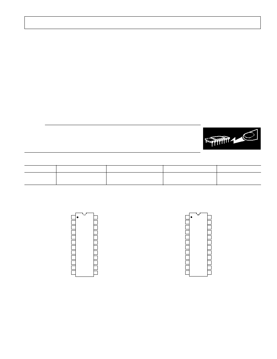
PIN CONFIGURATIONS
24-Lead TSSOP
TOP VIEW
(Not to Scale)
24
23
22
21
20
19
18
17
16
15
14
13
1
2
3
4
5
6
7
8
9
10
11
12
SYNC
RESET
DOUT
V
SS
S8
D8
S7
D7
S6
D6
S5
D5
SCLK
V
DD
DIN
GND
S1
D1
S2
D2
S3
D3
S4
D4
ADG714
TOP VIEW
(Not to Scale)
24
23
22
21
20
19
18
17
16
15
14
13
1
2
3
4
5
6
7
8
9
10
11
12
A0
RESET
A1
V
SS
S8
D8
S7
D7
S6
D6
S5
D5
SCL
V
DD
SDA
GND
S1
D1
S2
D2
S3
D3
S4
D4
ADG715
CAUTION
ESD (electrostatic discharge) sensitive device. Electrostatic charges as high as 4000 V readily
accumulate on the human body and test equipment and can discharge without detection. Although
the ADG714/ADG715 feature proprietary ESD protection circuitry, permanent damage may occur
on devices subjected to high-energy electrostatic discharges. Therefore, proper ESD precautions
are recommended to avoid performance degradation or loss of functionality.
WARNING!
ESD SENSITIVE DEVICE
ADG714/ADG715
8
REV. 0
ADG714 PIN FUNCTION DESCRIPTIONS
Pin No.
Mnemonic
Description
1
SCLK
Serial Clock Input. Data is clocked into the input shift register on the falling edge of the serial
clock input. These devices can accommodate serial input rates of up to 30 MHz.
2
V
DD
Positive Analog Supply Voltage.
3
DIN
Serial Data Input. Data is clocked into the 8-bit input register on the falling edge of the serial
clock input.
4
GND
Ground Reference.
5, 7, 9, 11, 14,
Sx
Source. May be an input or output.
16, 18, 20
6, 8, 10, 12, 13,
Dx
Drain. May be an input or output.
15, 17, 19
21
V
SS
Negative Analog Supply Voltage. For single supply operation this should be tied to GND.
22
DOUT
Serial Data Output. This allows a number a parts to be daisy chained. Data is clocked out of
the input shift register on the rising edge of SCLK. DOUT is an open-drain output that should be
pulled to the supply with an external pull-up resistor.
23
RESET
Active Low Control Input. Clears the input register and turns all switches to the OFF condition.
24
SYNC
Active Low Control Input. This is the frame synchronization signal for the input data. When
SYNC goes low, it powers on the SCLK and DIN buffers and the input shift register is enabled.
Data is transferred on the falling edges of the following clocks. Taking
SYNC high updates the
switches.
ADG715 PIN FUNCTION DESCRIPTIONS
Pin No.
Mnemonic
Description
1
SCL
Serial Clock Line. This is used in conjunction with the SDA line to clock data into the 8-bit input
shift register. Clock rates of up to 400 kbit/s can be accommodated with this 2-wire serial interface.
2
V
DD
Positive Analog Supply Voltage.
3
SDA
Serial Data Line. This is used in conjunction with the SCL line to clock data into the 8-bit input
shift register during the write cycle and used to readback one byte of data during the read cycle. It
is a bidirectional open-drain data line which should be pulled to the supply with an external pull-
up resistor.
4
GND
Ground Reference.
5, 7, 9, 11, 14,
Sx
Source. May be an input or output.
16, 18, 20
6, 8, 10, 12, 13,
Dx
Drain. May be an input or output.
15, 17, 19
21
V
SS
Negative Analog Supply Voltage. For single supply operation this should be tied to GND.
22
A1
Address Input. Sets the second least significant bit of the 7-bit slave address.
23
RESET
Active Low Control Input. Clears the input register and turns all switches to the OFF condition.
24
A0
Address Input. Sets the least significant bit of the 7-bit slave address.
ADG714/ADG715
9
REV. 0
V
DD
Most positive power supply potential.
V
SS
Most negative power supply in a dual supply
application. In single supply applications, this
should be tied to ground.
I
DD
Positive Supply Current.
I
SS
Negative Supply Current.
GND
Ground (0 V) Reference
S
Source Terminal. May be an input or output.
D
Drain Terminal. May be an input or output.
R
ON
Ohmic resistance between D and S.
R
ON
On-resistance match between any two channels,
i.e., R
ON
maxR
ON
min.
R
FLAT(ON)
Flatness is defined as the difference between the
maximum and minimum value of on-resistance
as measured over the specified analog signal range.
I
S
(OFF)
Source leakage current with the switch "OFF."
I
D
(OFF)
Drain leakage current with the switch "OFF."
I
D
, I
S
(ON)
Channel leakage current with the switch "ON."
V
D
(V
S
)
Analog voltage on terminals D and S.
C
S
(OFF)
"OFF" Switch Source Capacitance. Measured
with reference to ground.
C
D
(OFF)
"OFF" Switch Drain Capacitance. Measured
with reference to ground.
C
D
, C
S
(ON)
"ON" Switch Capacitance. Measured with ref-
erence to ground.
C
IN
Digital Input Capacitance.
t
ON
Delay time between loading new data to the
shift register and selected switches switching on.
t
OFF
Delay time between loading new data to the
shift register and selected switches switching off.
Off Isolation
A measure of unwanted signal coupling through
an "OFF" switch.
Crosstalk
A measure of unwanted signal which is coupled
through from one channel to another as a result
of parasitic capacitance.
Charge
A measure of the glitch impulse transferred
Injection
from the digital input to the analog output
during switching.
Bandwidth
The frequency at which the output is attenuated
by 3 dBs.
On Response
The frequency response of the "ON" switch.
Insertion Loss The loss due to the ON resistance of the switch.
Insertion Loss = 20 log
10
(V
OUT
with switch/
V
OUT
without switch.
V
INL
Maximum input voltage for Logic 0.
V
INH
Minimum input voltage for Logic 1.
I
INL
(I
INH
)
Input current of the digital input.
I
DD
Positive Supply Current.
TERMINOLOGY
ADG714/ADG715
10
REV. 0
Typical Performance Characteristics
V
D
, V
S
, DRAIN OR SOURCE VOLTAGE V
8
0
1
2
3
4
5
T
A
= 25 C
V
SS
= GND
7
6
5
4
3
2
1
0
ON RESISTANCE
V
DD
= 2.7V
V
DD
= 3.3V
V
DD
= 4.5V
V
DD
= 5.5V
Figure 3. On Resistance as a Function of V
D
(V
S
) Single
Supply
V
D
OR V
S
DRAIN OR SOURCE VOLTAGE V
3.3
T
A
= 25 C
0
ON RESISTANCE
2.7
2.1 1.5 0.9 0.3
0.3
0.9
1.5
2.1
2.7
3.3
8
7
6
5
4
3
2
1
V
DD
= +3.3V
V
SS
= 3.3V
V
DD
= +3.0V
V
SS
= 3.0V
V
DD
= +2.7V
V
SS
= 2.7V
Figure 4. On Resistance as a Function of V
D
(V
S
); Dual
Supply
V
D
OR V
S
DRAIN OR SOURCE VOLTAGE V
0
V
DD
= 5V
V
SS
= GND
0
ON RESISTANCE
+25 C
1
2
3
5
4
8
7
6
5
4
3
2
1
+85 C
40 C
Figure 5. On Resistance as a Function of V
D
(V
S
) for
Different Temperatures; V
DD
= 3 V
V
D
OR V
S
DRAIN OR SOURCE VOLTAGE V
0
V
DD
= 3V
V
SS
= GND
ON RESISTANCE
0.5
1.0
1.5
2.5
2.0
8
7
6
5
4
3
2
+85 C
40 C
3.0
+25 C
Figure 6. On Resistance as a Function of V
D
(V
S
) for
Different Temperatures; V
DD
= 5 V
V
D
OR V
S
DRAIN OR SOURCE VOLTAGE V
7
6
5
4
3
2
1
0
ON RESISTANCE
3.0 2.5 2.0 1.5 1.0
1.0
1.5
2.0
2.5
0.5
0
V
DD
= +3.0V
V
SS
= 3.0V
+85 C
+25 C
40 C
3.0
8
0.5
Figure 7. On Resistance as a Function of V
D
(V
S
) for
Different Temperatures; Dual Supply
V
D
OR V
S
Volts
0
CURRENT
nA
0
1
2
4
3
V
DD
= 5V
V
SS
= GND
T
A
= 25 C
5
0.04
0.02
0.02
0.04
I
S
, I
D
(ON)
I
D
(OFF)
I
S
(OFF)
Figure 8. Leakage Currents as a Function of V
D
(V
S
)
ADG714/ADG715
11
REV. 0
VOLTAGE V
0
CURRENT
nA
0
1
0.5
2
1.5
V
DD
= 3V
V
SS
= GND
T
A
= 25 C
3
0.04
0.02
0.02
0.04
I
D
(OFF)
I
S
(OFF)
I
S
, I
D
(ON)
2.5
Figure 9. Leakage Currents as a Function of V
D
(V
S
)
VOLTAGE
V
0
CURRENT
nA
3
2
1
3
0
V
DD
= +3V
V
SS
= 3V
T
A
= 25 C
I
D
(OFF)
I
S
(OFF)
I
S
, I
D
(ON)
0.04
0.02
0.02
0.04
2
1
Figure 10. Leakage Currents as a Function of V
D
(V
S
) Dual
Supply
TEMPERATURE
C
0
CURRENT
nA
10
20
30
70
40
0.1
0.05
0.05
0.1
60
50
I
S
, I
D
(ON)
I
D
(OFF)
I
S
(OFF)
V
DD
= +3V
V
SS
= 3V
V
D
= +2.25V/1.25V
V
S
= 1.25V/+2.25V
V
DD
= +5V
V
SS
= GND
V
D
= 4.5V/1V
V
S
= 1V/4.5V
80
Figure 11. Leakage Currents as Function of Temperature
TEMPERATURE
C
0
CURRENT
nA
10
20
30
70
40
0.1
0.05
0.05
0.1
60
50
I
D
, I
S
(ON)
I
S
(OFF)
I
D
(OFF)
V
DD
= 3V
V
SS
= GND
V
D
= 3V/1V
V
S
= 1V/3V
80
Figure 12. Leakage Currents as a Function of Temperature
FREQUENCY Hz
0
30k
ATTENUATION
dB
120
100
80
60
40
20
100k
1M
10M
100M
V
DD
= 5V
T
A
= 25 C
Figure 13. Off Isolation vs. Frequency
FREQUENCY Hz
14
300M
ATTENUATION
dB
12
10
8
6
4
0
2
100M
10M
1M
100k
30k
Figure 14. On Response vs. Frequency
ADG714/ADG715
12
REV. 0
FREQUENCY Hz
30k
ATTENUATION
dB
90
80
60
40
100k
1M
10M
100M
V
DD
= 5V
T
A
= 25 C
100
70
50
Figure 15. Crosstalk vs. Frequency
VOLTAGE V
3
T
A
= 25 C
10
0
20
Q
INJ
pC
V
DD
= +3.0V
V
SS
= 3.0V
V
DD
= +3.3V
V
SS
= GND
15
10
5
5
2
1
0
1
2
3
4
5
V
DD
= +5V
V
SS
= GND
Figure 16. Charge Injection vs. Source/Drain Voltage
TEMPERATURE
C
TIME
ns
10
20
30
70
40
45
40
60
50
V
SS
= GND
80
35
30
25
20
15
10
5
0
T
O N
, V
DD
= 5V
T
O F F
, V
DD
= 3V
T
O F F
, V
DD
= 5V
T
O N
, V
DD
= 3V
Figure 17. T
ON
/T
OFF
Times vs. Temperature for ADG714
GENERAL DESCRIPTION
The ADG714 and ADG715 are serially controlled, octal SPST
switches, controlled by either a 2- or 3-wire interface. Each bit
of the 8-bit serial word corresponds to one switch of the part. A
Logic 1 in the particular bit position turns on the switch, while a
Logic 0 turns the switch off. Because each switch is independently
controlled by an individual bit, this provides the option of having
any, all, or none of the switches ON.
When changing the switch conditions, a new 8-bit word is writ-
ten to the input shift register. Some of the bits may be the same
as the previous write cycle, as the user may not wish to change
the state of some switches. In order to minimize glitches on the
output of these switches, the part cleverly compares the state of
switches from the previous write cycle. If the switch is already
in the ON condition, and is required to stay ON, there will be
minimal glitches on the output of the switch.
POWER-ON RESET
On power-up of the device, all switches will be in the OFF con-
dition and the internal shift register is filled with zeros and will
remain so until a valid write takes place.
SERIAL INTERFACE
3-Wire Serial Interface
The ADG714 has a 3-wire serial interface (
SYNC, SCLK, and
DIN), that is compatible with SPI, QSPI, MICROWIRE
interface standards and most DSPs. Figure 1 shows the tim-
ing diagram of a typical write sequence.
Data is written to the 8-bit shift register via DIN under the con-
trol of the
SYNC and SCLK signals. Data may be written to
the shift register in more or less than eight bits. In each case
the shift register retains the last eight bits that were written.
When
SYNC goes low, the input shift register is enabled. Data
from DIN is clocked into the shift register on the falling edge of
SCLK. Each bit of the 8-bit word corresponds to one of the eight
switches. Figure 18 shows the contents of the input shift regis-
ter. Data appears on the DOUT pin on the rising edge of SCLK
suitable for daisy chaining, delayed of course by eight bits. When
all eight bits have been written into the shift register, the
SYNC
line is brought high again. The switches are updated with the
new configuration and the input shift register is disabled. With
SYNC held high, the input shift register is disabled, so further data
or noise on the DIN line will have no effect on the shift register.
S8
S7
S6
S5
S4
S3
S2
S1
DB7 (MSB)
DB0 (LSB)
DATA BITS
Figure 18. Input Shift Register Contents
SERIAL INTERFACE
2-Wire Serial Interface
The ADG715 is controlled via an I
2
C-compatible serial bus.
This device is connected to the bus as a slave device (no clock is
generated by the switch).
The ADG715 has a 7-bit slave address. The five MSBs are 10010
and the two LSBs are determined by the state of the A0 and
A1 pins.
ADG714/ADG715
13
REV. 0
A repeated write function gives the user flexibility to update the
matrix switch a number of times after addressing the part only
once. During the write cycle, each data byte will update the con-
figuration of the switches. For example, after the matrix switch
has acknowledged its address byte, and received one data byte,
the switches will update after the data byte; if another data byte
is written to the matrix switch while it is still the addressed slave
device, this data byte will also cause a switch configuration update.
Repeat read of the matrix switch is also allowed.
Input Shift Register
The input shift register is eight bits wide. Figure 18 illustrates
the contents of the input shift register. Data is loaded into the
device as an 8-bit word under the control of a serial clock input,
SCL. The timing diagram for this operation is shown in Figure
2. The 8-bit word consists of eight data bits, each controlling
one switch. MSB (Bit 7) is loaded first.
Write Operation
When writing to the ADG715, the user must begin with an address
byte and R/
W bit, after which the switch will acknowledge that
it is prepared to receive data by pulling SDA low. This address
byte is followed by the 8-bit word. The write operation for the
switch is shown in the Figure 19 below.
READ Operation
When reading data back from the ADG715, the user must begin
with an address byte and R/
W bit, after which the switch will
acknowledge that it is prepared to transmit data by pulling SDA
low. The readback operation is a single byte that consists of the
eight data bits in the input register. The read operation for the
part is shown in Figure 20.
SCL
SDA
S8
S7
S6
S5
S4
S3
S2
S1
0
0
1
0
A0
R/W
STOP
COND
BY
MASTER
ACK
BY
ADG715
START
COND
BY
MASTER
ADDRESS BYTE
DATA BYTE
ACK
BY
ADG715
A1
1
Figure 19. ADG715 Write Sequence
SCL
SDA
S8
S7
S6
S5
S4
S3
S2
S1
0
0
1
0
A0
R/
W
STOP
COND
BY
MASTER
ACK
BY
ADG715
START
COND
BY
MASTER
ADDRESS BYTE
DATA BYTE
NO ACK
BY
MASTER
A1
1
Figure 20. ADG715 Readback Sequence
The 2-wire serial bus protocol operates as follows:
1. The master initiates data transfer by establishing a START
condition, which is when a high-to-low transition on the
SDA line occurs while SCL is high. The following byte is the
address byte that consists of the 7-bit slave address followed
by a R/
W bit (this bit determines whether data will be read
from or written to the slave device).
The slave whose address corresponds to the transmitted address
responds by pulling the SDA line low during the ninth clock
pulse (this is termed the acknowledge bit). At this stage,
all other devices on the bus remain idle while the selected
device waits for data to be written to or read from its serial
register. If the R/
W bit is high, the master will read from the
slave device. However, if the R/
W bit is low, the master will
write to the slave device.
2. Data is transmitted over the serial bus in sequences of nine
clock pulses (eight data bits followed by an acknowledge bit).
The transitions on the SDA line must occur during the
low period of SCL and remain stable during the high
period of SCL.
3. When all data bits have been read or written, a STOP con-
dition is established by the master. A STOP condition is
defined as a low-to-high transition on the SDA line while
SCL is high. In write mode, the master will pull the SDA
line high during the tenth clock pulse to establish a STOP
condition. In read mode, the master will issue a no acknowledge
for the ninth clock pulse (i.e., the SDA line remains high).
The master will then bring the SDA line low before the tenth
clock pulse and then high during the tenth clock pulse to estab-
lish a STOP condition.
See Figure 19 for a graphical explanation of the serial interface.
ADG714/ADG715
14
REV. 0
SDA
SCL
SDA
SCL
SDA
SCL
SDA
SCL
A1
A0
A1
A0
A1
A0
A1
A0
ADG715
ADG715
ADG715
ADG715
SDA
SCL
V
DD
V
DD
V
DD
MASTER
R
P
R
P
V
DD
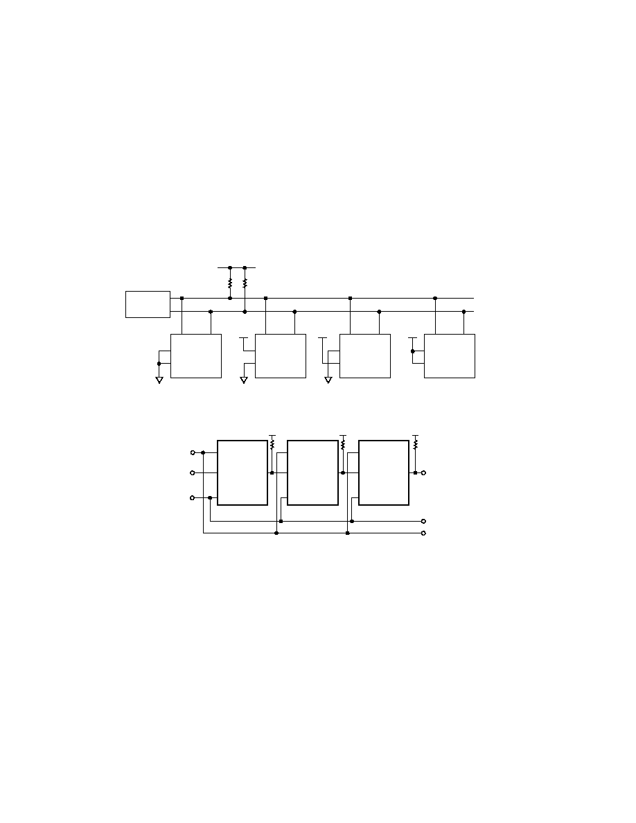
Figure 21. Multiple ADG715s On One Bus
-
SCLK
DIN
DOUT
ADG714
SYNC
TO
OTHER
SERIAL
DEVICES
SCLK
DIN
SYNC
SCLK
DIN
DOUT
ADG714
SYNC
SCLK
DIN
DOUT
ADG714
SYNC
V
DD
V
DD
V
DD
R
R
R
Figure 22. Multiple ADG714 Devices in a Daisy-Chained Configuration
APPLICATIONS
Multiple Devices On One Bus
Figure 21 shows four ADG715 devices on the same serial bus.
Each has a different slave address since the state of their A0 and
A1 pins is different. This allows each switch to be written to or
read from independently.
Daisy-Chaining Multiple ADG714s
A number of ADG714 switches may be daisy-chained simply by
using the DOUT pin. Figure 22 shows a typical implementa-
tion. The
SYNC pin of all three parts in the example are tied
together. When
SYNC is brought low, the input shift registers
of all parts are enabled, data is written to the parts via DIN, and
clocked through the shift registers. When the transfer is complete,
SYNC is brought high and all switches are updated simulta-
neously. Further shift registers may be added in series.
Power Supply Sequencing
When using CMOS devices, care must be taken to ensure correct
power-supply sequencing. Incorrect power-supply sequencing
can result in the device being subjected to stresses beyond those
maximum ratings listed in the data sheet. Digital and analog inputs
should always be applied after power supplies and ground. In dual
supply applications, if digital or analog inputs may be applied to
the device prior to the V
DD
and V
SS
supplies, the addition of a
Schottky diode connected between V
SS
and GND will ensure
that the device powers on correctly. For single supply operation,
V
SS
should be tied to GND as close to the device as possible.
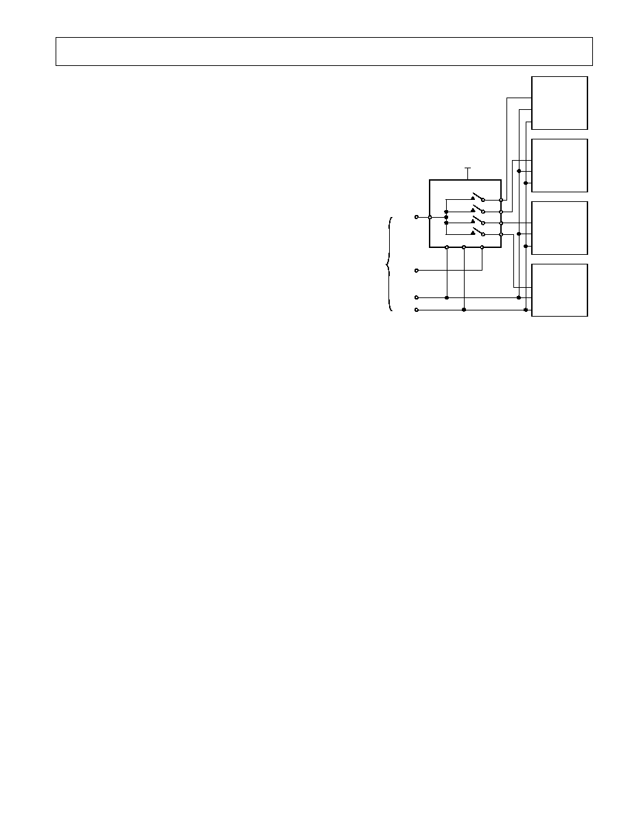
Decoding Multiple ADG714s Using an ADG739
The dual 4-channel ADG739 multiplexer can be used to multiplex
a single chip select line in order to provide chip selects for up to
ADG714/ADG715
15
REV. 0
four devices on the SPI bus. Figure 23 illustrates the ADG739 and
multiple ADG714s in such a typical configuration. All devices
receive the same serial clock and serial data, but only one device
will receive the
SYNC signal at any one time. The ADG739 is a
serially controlled device also. One bit programmable pin of the
microcontroller is used to enable the ADG739 via
SYNC2,
while another bit programmable pin is used as the chip select for
the other serial devices,
SYNC1. Driving SYNC2 low enables
changes to be made to the addressed serial devices. By bringing
SYNC1 low, the selected serial device hanging from the SPI bus
will be enabled and data will be clocked into its shift register on
the falling edges of SCLK. The convenient design of the matrix
switch allows for different combinations of the four serial
devices to be addressed at any one time. If more devices need
to be addressed via one chip select line, the ADG738 is an 8-
channel device and would allow further expansion of the chip
select scheme. There may be some digital feedthrough from the
digital input lines because SCLK and DIN are permanently
connected to each device. Using a burst clock will minimize the
effects of digital feedthrough on the analog channels.
OTHER
SPI
DEVICE
DIN
SCLK
DIN
SCLK
DIN
SCLK
DIN
SCLK
ADG714
ADG714
SCLK DIN
S1A
S4A
DA
1/2 of ADG739
SYNC
S3A
S2A
FROM
CONTROLLER
OR DSP
SYNC1
SYNC2
SYNC
SYNC
SYNC
SYNC
SCLK
DIN
V
DD
OTHER
SPI
DEVICE
Figure 23. Addressing Multiple ADG714s Using an
ADG739
16
C37682.54/00 (rev. 0) 00043
PRINTED IN U.S.A.
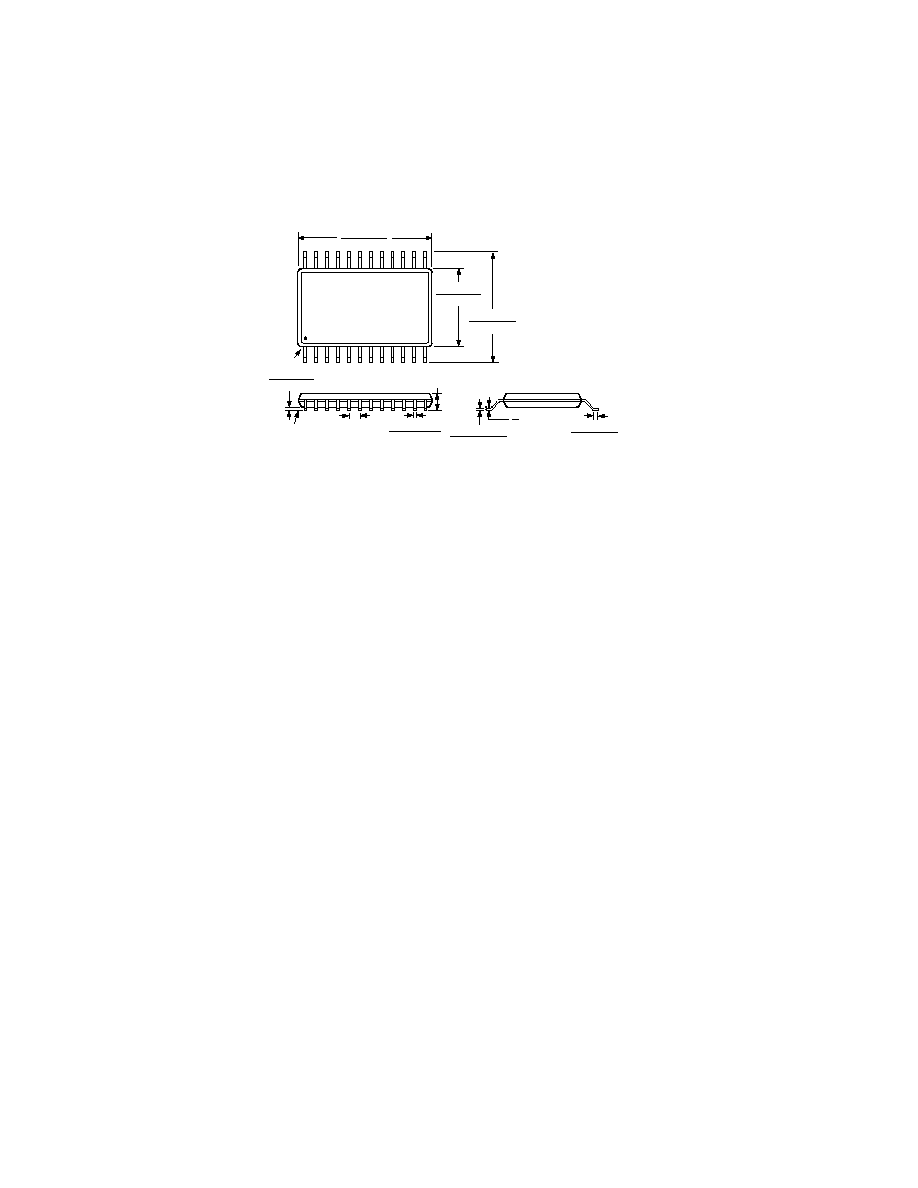
OUTLINE DIMENSIONS
Dimensions shown in inches and (mm).
24-Lead TSSOP
(RU-24)
24
13
12
1
0.256 (6.50)
0.246 (6.25)
0.177 (4.50)
0.169 (4.30)
PIN 1
0.311 (7.90)
0.303 (7.70)
SEATING
PLANE
0.006 (0.15)
0.002 (0.05)
0.0118 (0.30)
0.0075 (0.19)
0.0256 (0.65)
BSC
0.0433 (1.10)
MAX
0.0079 (0.20)
0.0035 (0.090)
0.028 (0.70)
0.020 (0.50)
8
0
ADG714/ADG715
REV. 0