 | ÐлекÑÑоннÑй компоненÑ: ADG738 | СкаÑаÑÑ:  PDF PDF  ZIP ZIP |
Äîêóìåíòàöèÿ è îïèñàíèÿ www.docs.chipfind.ru
ADG738/ADG739
a
REV. 0
Information furnished by Analog Devices is believed to be accurate and
reliable. However, no responsibility is assumed by Analog Devices for its
use, nor for any infringements of patents or other rights of third parties
which may result from its use. No license is granted by implication or
otherwise under any patent or patent rights of Analog Devices.
CMOS, Low-Voltage, 3-Wire
Serially-Controlled, Matrix Switches
One Technology Way, P.O. Box 9106, Norwood, MA 02062-9106, U.S.A.
Tel: 781/329-4700
World Wide Web Site: http://www.analog.com
Fax: 781/326-8703
© Analog Devices, Inc., 2000
FEATURES
3-Wire Serial Interface
2.7 V to 5.5 V Single Supply
2.5 On Resistance
0.75 On-Resistance Flatness
100 pA Leakage Currents
Single 8-to-1 Multiplexer ADG738
Dual 4-to-1 Multiplexer ADG739
Power-On Reset
TTL/CMOS-Compatible
APPLICATIONS
Data Acquisition Systems
Communication Systems
Relay Replacement
Audio and Video Switching
GENERAL DESCRIPTION
The ADG738 and ADG739 are CMOS analog matrix switches
with a serially-controlled 3-wire interface. The ADG738 is an
8-channel matrix switch, while the ADG739 is a dual 4-channel
matrix switch. On resistance is closely matched between switches
and very flat over the full signal range.
The ADG738 and ADG739 utilize a 3-wire serial interface that
is compatible with SPITM, QSPITM, MICROWIRETM, and some
DSP interface standards. The output of the shift register DOUT
enables a number of these parts to be daisy-chained. On power-up,
the internal shift register contains all zeros and all switches
are in the OFF state.
Each switch conducts equally well in both directions when on,
making these parts suitable for both multiplexing and demulti-
plexing applications. As each switch is turned on or off by a
separate bit, these parts can also be configured as a type of switch
array, where any, all, or none of the eight switches may be closed
at any time. The input signal range extends to the supply rails.
All channels exhibit break-before-make switching action,
preventing momentary shorting when switching channels.
The ADG738 and ADG739 are available in 16-lead TSSOP
packages.
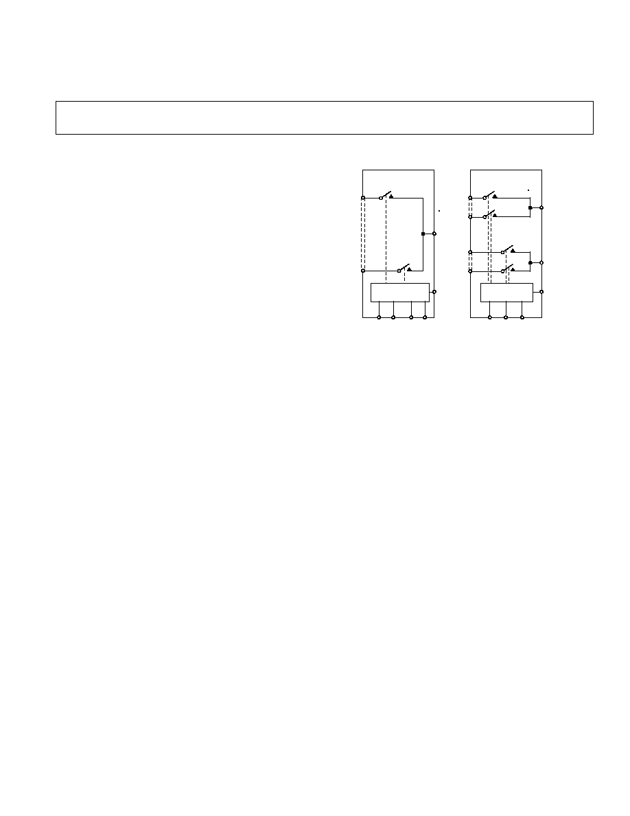
FUNCTIONAL BLOCK DIAGRAMS
S1
S8
SCLK
D
DIN
SYNC
ADG738
S1A
SCLK
DA
DIN
S4A
S1B
S4B
DB
ADG739
RESET
DOUT
DOUT
SYNC
INPUT SHIFT
REGISTER
INPUT SHIFT
REGISTER
SPI and QSPI are trademarks of Motorola, Inc.
MICROWIRE is a trademark of National Semiconductor Corporation.
PRODUCT HIGHLIGHTS
1. 3-Wire Serial Interface.
2. Single Supply Operation. The ADG738 and ADG739 are
fully specified and guaranteed with 3 V and 5 V supply rails.
3. Low On Resistance, 2.5
typical.
4. Any configuration of switches may be on or off at any one time.
5. Guaranteed Break-Before-Make Switching Action.
6. Small 16-lead TSSOP Package.
2
REV. 0
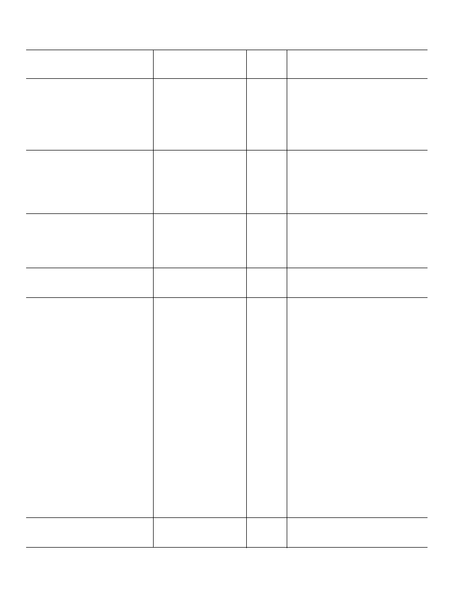
ADG738/ADG739SPECIFICATIONS
1
(V
DD
= 5 V 10%, GND = 0 V, unless otherwise noted.)
B Version
40 C
Parameter
25 C
to +85 C
Unit
Test Conditions/Comments
ANALOG SWITCH
Analog Signal Range
0 V to V
DD
V
On Resistance (R
ON
)
2.5
typ
V
S
= 0 V to V
DD
, I
S
= 10 mA;
4.5
5
max
Test Circuit 1
On-Resistance Match Between
0.4
typ
V
S
= 0 V to V
DD,
I
S
= 10 mA
Channels (
R
ON
)
0.8
max
On-Resistance Flatness (R
FLAT(ON)
)
0.75
typ
V
S
= 0 V to V
DD
, I
S
= 10 mA
1.2
max
LEAKAGE CURRENTS
V
DD
= 5.5 V
Source OFF Leakage I
S
(OFF)
±0.01
nA typ
V
D
= 4.5 V/1 V, V
S
= 1 V/4.5 V;
±0.1
±0.3
nA max
Test Circuit 2
Drain OFF Leakage I
D
(OFF)
±0.01
nA typ
V
D
= 4.5 V/1 V, V
S
= 1 V/4.5 V;
±0.1
±1
nA max
Test Circuit 3
Channel ON Leakage I
D
, I
S
(ON)
±0.01
nA typ
V
D
= V
S
= 1 V/4.5 V, Test Circuit 4
±0.1
±1
nA max
DIGITAL INPUTS
Input High Voltage, V
INH
2.4
V min
Input Low Voltage, V
INL
0.8
V max
Input Current, I
INL
or I
INH
0.005
µA typ
V
IN
= V
INL
or V
INH
±0.1
µA max
C
IN
, Digital Input Capacitance
3
pF typ
DIGITAL OUTPUT
Output Low Voltage
0.4
max
I
SINK
= 6 mA
C
OUT
, Digital Output Capacitance
4
pF typ
DYNAMIC CHARACTERISTICS
2
t
ON
20
ns typ
R
L
= 300
, C
L
= 35 pF, Test Circuit 5;
32
ns max
V
S1
= 3 V
t
OFF
10
ns typ
R
L
= 300
, C
L
= 35 pF, Test Circuit 5;
17
ns max
V
S1
= 3 V
Break-Before-Make Time Delay, t
D
9
ns typ
R
L
= 300
, C
L
= 35 pF;
1
ns min
V
S1
= V
S8
= 3 V, Test Circuit 5
Charge Injection
±3
pC typ
V
S
= 2.5 V, R
S
= 0
, C
L
= 1 nF;
Test Circuit 6
Off Isolation
55
dB typ
R
L
= 50
, C
L
= 5 pF, f = 10 MHz;
75
dB typ
R
L
= 50
, C
L
= 5 pF, f = 1 MHz;
Test Circuit 8
Channel-to-Channel Crosstalk
55
dB typ
R
L
= 50
, C
L
= 5 pF, f = 10 MHz;
75
dB typ
R
L
= 50
, C
L
= 5 pF, f = 1 MHz;
Test Circuit 7
3 dB Bandwidth
ADG738
65
MHz typ
R
L
= 50
, C
L
= 5 pF, Test Circuit 8
ADG739
100
MHz typ
C
S
(OFF)
13
pF typ
C
D
(OFF)
ADG738
85
pF typ
ADG739
42
pF typ
C
D
, C
S
(ON)
ADG738
96
pF typ
ADG739
48
pF typ
POWER REQUIREMENTS
V
DD
= 5.5 V
I
DD
10
µA typ
Digital Inputs = 0 V or 5.5 V
20
µA max
NOTES
1
Temperature range is as follows: B Version: 40
°C to +85°C.
2
Guaranteed by design, not subject to production test.
Specifications subject to change without notice.

3
REV. 0
ADG738/ADG739
B Version
40 C
Parameter
25 C
to +85 C
Unit
Test Conditions/Comments
ANALOG SWITCH
Analog Signal Range
0 V to V
DD
V
On Resistance (R
ON
)
6
typ
V
S
= 0 V to V
DD
, I
S
= 10 mA;
11
12
max
Test Circuit 1
On-Resistance Match Between
0.4
typ
V
S
= 0 V to V
DD
, I
S
= 10 mA
Channels (
R
ON
)
1.2
max
On-Resistance Flatness (R
FLAT(ON)
)
3.5
typ
V
S
= 0 V to V
DD
, I
S
= 10 mA
LEAKAGE CURRENTS
V
DD
= 3.3 V
Source OFF Leakage I
S
(OFF)
±0.01
nA typ
V
S
= 3 V/1 V, V
D
= 1 V/3 V;
±0.1
±0.3
nA max
Test Circuit 2
Drain OFF Leakage I
D
(OFF)
±0.01
nA typ
V
D
= 3 V/1 V, V
D
= 1 V/3 V;
±0.1
±1
nA max
Test Circuit 3
Channel ON Leakage I
D
, I
S
(ON)
±0.01
nA typ
V
D
= V
S
= 3 V/1 V, Test Circuit 4
±0.1
±1
nA max
DIGITAL INPUTS
Input High Voltage, V
INH
2.0
V min
Input Low Voltage, V
INL
0.4
V max
Input Current, I
INL
or I
INH
0.005
µA typ
V
IN
= V
INL
or V
INH
±0.1
µA max
C
IN
, Digital Input Capacitance
3
pF typ
DIGITAL OUTPUT
Output Low Voltage
0.4
max
I
SINK
= 6 mA
C
OUT
, Digital Output Capacitance
4
pF typ
DYNAMIC CHARACTERISTICS
2
t
ON
40
ns typ
R
L
= 300
, C
L
= 35 pF, Test Circuit 5;
70
ns max
V
S1
= 2 V
t
OFF
14
ns typ
R
L
= 300
, C
L
= 35 pF, Test Circuit 5;
25
ns max
V
S1
= 2 V
Break-Before-Make Time Delay, t
D
12
ns typ
R
L
= 300
, C
L
= 35 pF;
1
ns min
V
S
= 2 V, Test Circuit 5
Charge Injection
±3
pC typ
V
S
= 1.5 V, R
S
= 0
, C
L
= 1 nF;
Test Circuit 6
Off Isolation
55
dB typ
R
L
= 50
, C
L
= 5 pF, f = 10 MHz;
75
dB typ
R
L
= 50
, C
L
= 5 pF, f = 1 MHz;
Test Circuit 8
Channel-to-Channel Crosstalk
55
dB typ
R
L
= 50
, C
L
= 5 pF, f = 10 MHz;
75
dB typ
R
L
= 50
, C
L
= 5 pF, f = 1 MHz;
Test Circuit 7
3 dB Bandwidth
ADG738
65
MHz typ
R
L
= 50
, C
L
= 5 pF, Test Circuit 8
ADG739
100
MHz typ
C
S
(OFF)
13
pF typ
C
D
(OFF)
ADG738
85
pF typ
ADG739
42
pF typ
C
D
, C
S
(ON)
ADG738
96
pF typ
ADG739
48
pF typ
POWER REQUIREMENTS
V
DD
= 3.3 V
I
DD
10
µA typ
Digital Inputs = 0 V or 3.3 V
20
µA max
NOTES
1
Temperature ranges are as follows: B Versions: 40
°C to +85°C.
2
Guaranteed by design, not subject to production test.
Specifications subject to change without notice.
(V
DD
= 3 V 10%, GND = 0 V, unless otherwise noted.)
SPECIFICATIONS
1
4
REV. 0
ADG738/ADG739
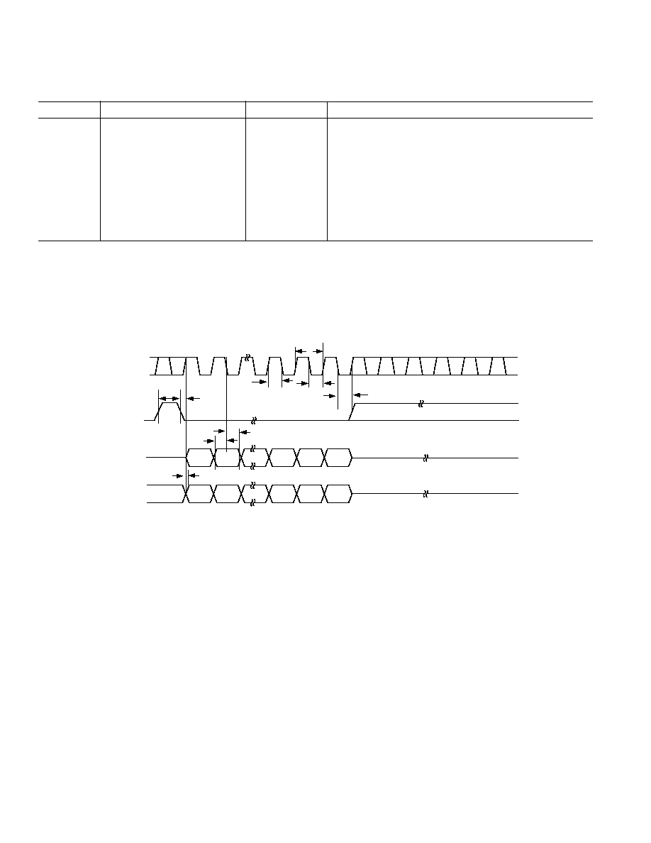
TIMING CHARACTERISTICS
1, 2
Parameter
Limit at T
MIN
, T
MAX
Unit
Conditions/Comments
f
SCLK
30
MHz max
SCLK Cycle Frequency
t
1
33
ns min
SCLK Cycle Time
t
2
13
ns min
SCLK High Time
t
3
13
ns min
SCLK Low Time
t
4
0
ns min
SYNC to SCLK Active Edge Setup Time
t
5
5
ns min
Data Setup Time
t
6
4.5
ns min
Data Hold Time
t
7
0
ns min
SCLK Falling Edge to
SYNC Rising Edge
t
8
33
ns min
Minimum
SYNC High Time
t
9
3
20
ns min
SCLK Rising Edge to DOUT Valid
NOTES
1
See Figure 1.
2
All input signals are specified with tr = tf = 5 ns (10% to 90% of V
DD
) and timed from a voltage level of (V
IL
+ V
IH
)/2.
3
C
L
= 20 pF, R
L
= 1 k
.
Specifications subject to change without notice.
SCLK
SYNC
DIN
DB7
DB0
DB7
1
DB0
1
DOUT
NOTE
1
DATA FROM LAST WRITE CYCLE
t
3
t
2
t
1
t
4
t
8
t
6
t
5
t
9
t
7
Figure 1. 3-Wire Serial Interface Timing Diagram
(V
DD
= 2.7 V to 5.5 V. All specifications 40 C to +85 C, unless otherwise noted.)
ADG738/ADG739
5
REV. 0
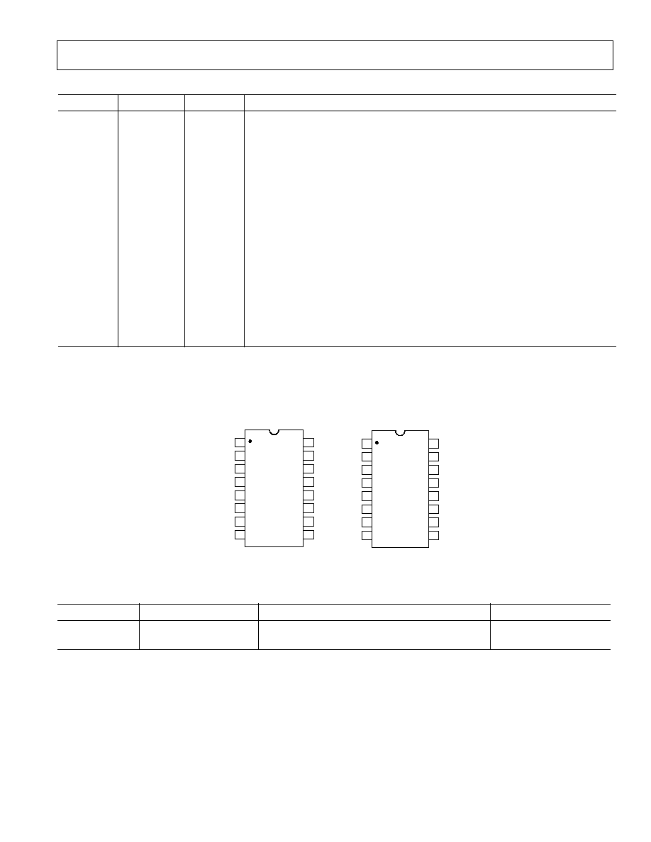
PIN CONFIGURATIONS
SCLK
RESET
S2
S3
S4
S1
D
1
2
16
15
5
6
7
12
11
10
3
4
14
13
8
9
TOP VIEW
(Not to Scale)
SYNC
DOUT
S5
S6
S7
GND
V
DD
S8
DIN
ADG738
SCLK
SYNC
DIN
DOUT
GND
S2A
S3A
S2B
S3B
S4B
S1A
V
DD
S1B
DA
DB
TOP VIEW
(Not to Scale)
S4A
1
2
16
15
5
6
7
12
11
10
3
4
14
13
8
9
ADG739
PIN FUNCTION DESCRIPTIONS
ADG738
ADG739
Mnemonic
Function
1
1
SCLK
Serial Clock Input. Data is clocked into the input shift register on the falling edge of the
serial clock input. These devices can accommodate serial input rates of up to 30 MHz.
2
RESET
Active low control input that clears the input register and turns all switches to the OFF
condition.
3
3
DIN
Serial Data Input. Data is clocked into the 8-bit input register on the falling edge of the
serial clock input.
4, 5, 6, 7
4, 5, 6, 7
Sxx
Source. May be an input or output.
8
8, 9
Dx
Drain. May be an input or output.
9, 10, 11, 12
10, 11, 12, 13
Sxx
Source. May be an input or output.
13
14
V
DD
Power Supply Input. These parts can be operated from a supply of 2.7 V to 5.5 V.
14
15
GND
Ground Reference.
15
16
DOUT
Data Output. This allows a number a parts to be daisy-chained. Data is clocked out of
the input shift register on the rising edge of SCLK. This is an open drain output which
should be pulled to the supply with an external resistor.
16
2
SYNC
Active Low Control Input. This is the frame synchronization signal for the input data.
When
SYNC goes low, it powers on the SCLK and DIN buffers and the input shift
register is enabled. Data is transferred on the falling edges of the following clocks.
Taking
SYNC high updates the switch conditions.
ORDERING GUIDE
Model
Temperature Range
Package Description
Package Option
ADG738BRU
40
°C to +85°C
Thin Shrink Small Outline Package (TSSOP)
RU-16
ADG739BRU
40
°C to +85°C
Thin Shrink Small Outline Package (TSSOP)
RU-16
6
REV. 0
ADG738/ADG739
ABSOLUTE MAXIMUM RATINGS
1
(T
A
= 25
°C unless otherwise noted.)
V
DD
to GND . . . . . . . . . . . . . . . . . . . . . . . . . . 0.3 V to +7 V
Analog, Digital Inputs
2
. . . . . . . . . . 0.3 V to V
DD
+ 0.3 V or
30 mA, Whichever Occurs First
Peak Current, S or D . . . . . . . . . . . . . . . . . . . . . . . . . . 100 mA
(Pulsed at 1 ms, 10% Duty Cycle max)
Continuous Current, Each S . . . . . . . . . . . . . . . . . . . . . 30 mA
Continuous Current D, ADG739 . . . . . . . . . . . . . . . . . 80 mA
Continuous Current D, ADG738 . . . . . . . . . . . . . . . . 120 mA
Operating Temperature Range
Industrial (B Version) . . . . . . . . . . . . . . . . 40
°C to +85°C
Storage Temperature Range . . . . . . . . . . . . 65
°C to +150°C
Junction Temperature . . . . . . . . . . . . . . . . . . . . . . . . . . 150
°C
TSSOP Package
JA
Thermal Impedance . . . . . . . . . . . . . . . . . . . 150.4
°C/W
JC
Thermal Impedance . . . . . . . . . . . . . . . . . . . . 27.6
°C/W
Lead Temperature, Soldering (10 seconds) . . . . . . . . . . 300
°C
IR Reflow, Peak Temperature . . . . . . . . . . . . . . . . . . . . 220
°C
NOTES
1
Stresses above those listed under Absolute Maximum Ratings may cause perma-
nent damage to the device. This is a stress rating only; functional operation of the
device at these or any other conditions above those listed in the operational
sections of this specification is not implied. Exposure to absolute maximum rating
conditions for extended periods may affect device reliability. Only one absolute
maximum rating may be applied at any one time.
2
Overvoltages at IN, S or D will be clamped by internal diodes. Current should be
limited to the maximum ratings given.
TERMINOLOGY
C
D
, C
S
(ON) "ON" Switch Capacitance. Measured with refer-
ence to ground.
C
IN
Digital Input Capacitance.
t
ON
Delay time between the 50% and 90% points
of the
SYNC rising edge and the switch "ON"
condition.
t
OFF
Delay time between the 50% and 90% points
of the
SYNC rising edge and the switch "OFF"
condition.
t
D
"OFF" time measured between the 80% points of
both switches when switching from one switch to
another.
Charge
A measure of the glitch impulse transferred from
Injection
the digital input to the analog output during
switching.
Off Isolation
A measure of unwanted signal coupling through
an "OFF" switch.
Crosstalk
A measure of unwanted signal which is coupled
through from one channel to another as a result
of parasitic capacitance.
Bandwidth
The frequency at which the output is attenuated
by 3 dBs.
On Response The frequency response of the "ON" switch.
Insertion
The loss due to the ON resistance of the switch.
Loss
V
DD
Most Positive Power Supply Potential.
I
DD
Positive Supply Current.
GND
Ground (0 V) Reference.
S
Source Terminal. May be an input or output.
D
Drain Terminal. May be an input or output.
V
D
(V
S
)
Analog Voltage on Terminals D, S.
R
ON
Ohmic Resistance between D and S.
R
ON
On Resistance Match Between any Two Chan-
nels, i.e., R
ON
max R
ON
min.
R
FLAT(ON)
Flatness is defined as the difference between the
maximum and minimum value of on resistance
as measured over the specified analog signal range.
I
S
(OFF)
Source Leakage Current with the Switch "OFF."
I
D
(OFF)
Drain Leakage Current with the Switch "OFF."
I
D
, I
S
(ON)
Channel Leakage Current with the Switch "ON."
V
INL
Maximum Input Voltage for Logic "0."
V
INH
Minimum Input Voltage for Logic "1."
I
INL
(I
INH
)
Input Current of the Digital Input.
C
S
(OFF)
"OFF" Switch Source Capacitance. Measured
with reference to ground.
C
D
(OFF)
"OFF" Switch Drain Capacitance. Measured
with reference to ground.
CAUTION
ESD (electrostatic discharge) sensitive device. Electrostatic charges as high as 4000 V readily
accumulate on the human body and test equipment and can discharge without detection. Although
the ADG738/ADG739 feature proprietary ESD protection circuitry, permanent damage may occur
on devices subjected to high-energy electrostatic discharges. Therefore, proper ESD precautions
are recommended to avoid performance degradation or loss of functionality.
WARNING!
ESD SENSITIVE DEVICE
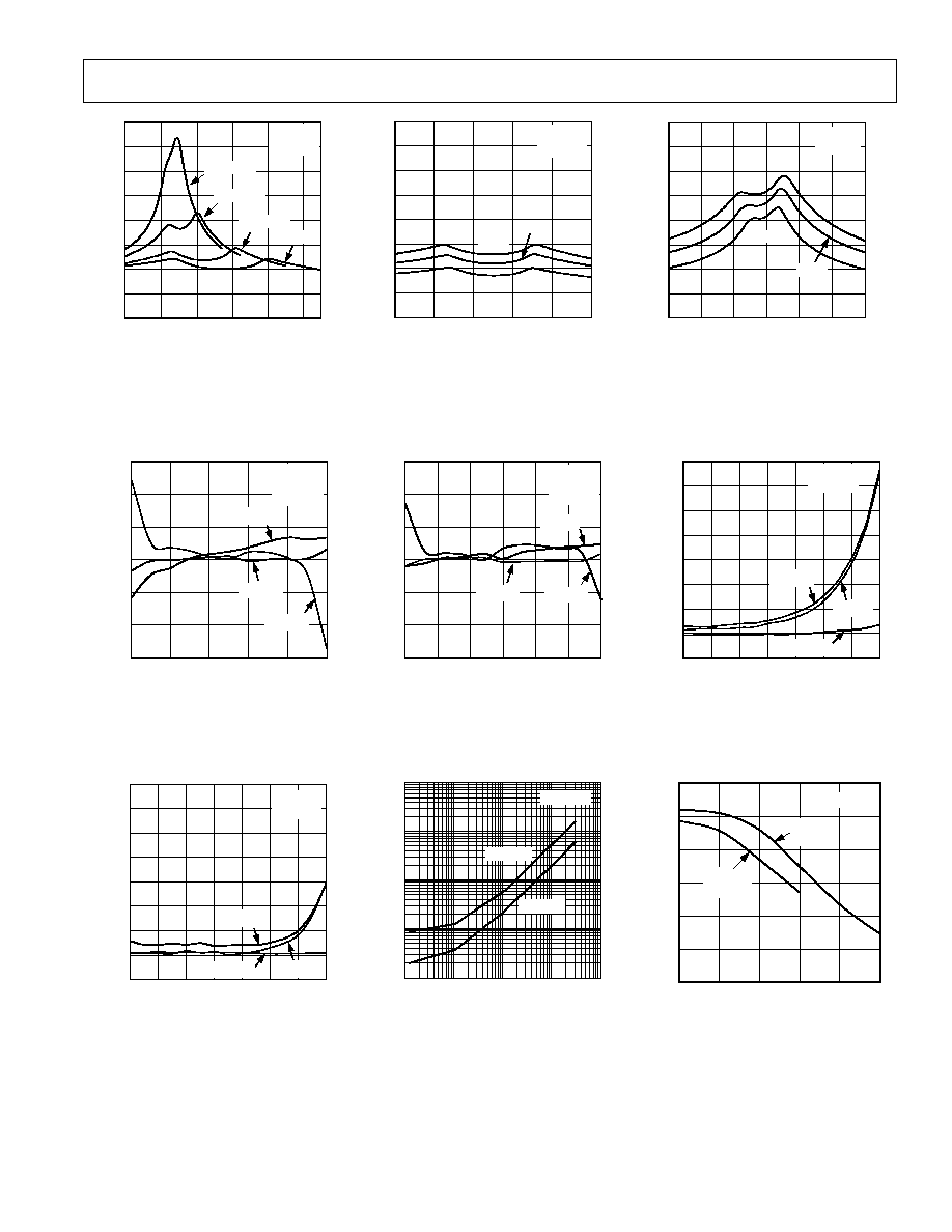
Typical Performance CharacteristicsADG738/ADG739
7
REV. 0
V
D
, V
S
, DRAIN OR SOURCE VOLTAGE V
8
0
1
2
3
4
7
6
5
4
3
2
1
0
ON RESISTANCE
T
A
= 25 C
V
SS
= 0V
V
DD
= 4.5V
V
DD
= 5.5V
V
DD
= 3.3V
V
DD
= 2.7V
5
Figure 2. On Resistance as a Function
of V
D
(V
S
)
V
D
(V
S)
Volts
0
1
0.12
CURRENT
nA
2
3
4
5
0.08
0.04
0.00
0.04
0.08
0.12
V
DD
= 5V
V
SS
= 0V
T
A
= 25 C
I
D
(ON)
I
S
(OFF)
I
D
(OFF)
Figure 5. Leakage Currents as a Func-
tion of V
D
(V
S
)
TEMPERATURE
C
15
CURRENT
nA
0.05
0.00
0.05
0.10
0.15
0.20
0.25
0.30
0.35
25
35
45
55
65
75
85
V
DD
= 3V
V
SS
= 0V
I
D
(OFF)
I
D
(ON)
I
S
(OFF)
Figure 8. Leakage Currents as a Func-
tion of Temperature
V
D
OR V
S
DRAIN OR SOURCE VOLTAGE V
0
1
2
3
4
5
7
6
5
4
3
2
1
0
ON RESISTANCE
+25 C
8
V
DD
= 5V
V
SS
= 0V
40 C
+85 C
Figure 3. On Resistance as a Function
of V
D
(V
S
) for Different Temperatures
V
D
(V
S)
Volts
0
0.5
0.12
CURRENT
nA
1.0
1.5
2.0
3.0
0.08
0.04
0.00
0.04
0.08
0.12
2.5
V
DD
= 3V
V
SS
= 0V
T
A
= 25 C
I
D
(ON)
I
D
(OFF)
I
S
(OFF)
Figure 6. Leakage Currents as a Func-
tion of V
D
(V
S
)
FREQUENCY Hz
CURRENT
A
1
10k
10
100
1m
10m
100k
1M
10M
100M
T
A
= 25 C
V
DD
= 5V
V
DD
= 3V
Figure 9. Input Currents vs. Switching
Frequency
V
D
OR V
S
DRAIN OR SOURCE VOLTAGE V
0
0.5
7
6
5
4
3
2
1
0
ON RESISTANCE
1.0
1.5
2.0
2.5
3.0
8
+25 C
40 C
+85 C
V
DD
= 3V
V
SS
= 0V
Figure 4. On Resistance as a Function
of V
D
(V
S
) for Different Temperatures
TEMPERATURE
C
15
CURRENT
nA
0.05
0.00
0.05
0.10
0.15
0.20
0.25
0.30
0.35
25
35
45
55
65
75
85
V
DD
= 5V
V
SS
= 0V
I
D
(ON)
I
D
(OFF)
I
S
(OFF)
Figure 7. Leakage Currents as a Func-
tion of Temperature
VOLTAGE Volts
Q
INJ
pC
40
0
30
20
10
0
10
20
1
2
3
4
5
T
A
= 25 C
V
DD
= 3V
V
SS
= 0V
V
DD
= 5V
V
SS
= 0V
Figure 10. Charge Injection vs. Source
Voltage
8
REV. 0
ADG738/ADG739
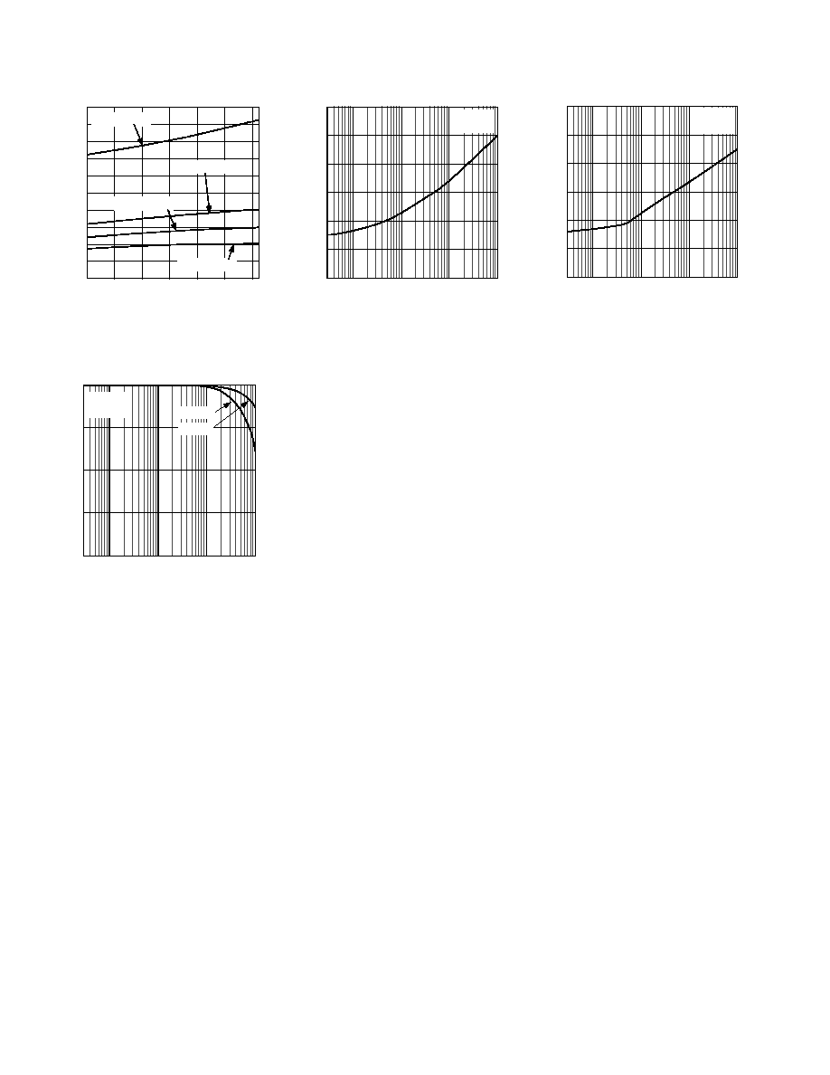
TEMPERATURE
C
40
TIME
ns
0
5
10
15
20
25
30
35
40
20
0
20
40
60
80
T
ON
, V
DD
= 3V
T
ON
, V
DD
= 5V
T
OFF
, V
DD
= 3V
T
OFF
, V
DD
= 5V
45
50
Figure 11. T
ON
/T
OFF
Times vs.
Temperature
FREQUENCY Hz
0
30k
ATTENUATION
dB
5
100k
1M
10M
100M
10
15
20
V
DD
= 5V
T
A
= 25 C
ADG738
ADG739
Figure 14. On Response vs. Frequency
FREQUENCY Hz
0
30k
ATTENUATION
dB
20
40
60
80
100
120
100k
1M
10M
100M
V
DD
= 5V
T
A
= 25 C
Figure 12. Off Isolation vs. Frequency
FREQUENCY Hz
0
30k
ATTENUATION
dB
20
40
60
80
100
120
100k
1M
10M
100M
V
DD
= 5V
T
A
= 25 C
Figure 13. Crosstalk vs. Frequency
ADG738/ADG739
9
REV. 0
GENERAL DESCRIPTION
The ADG738 and ADG739 are serially controlled, 8-channel
and dual 4-channel Matrix Switches respectively. While provid-
ing the normal multiplexing and demultiplexing functions, these
parts also provide the user with more flexibility as to where their
signal may be routed. Each bit of the 8-bit serial word corresponds
to one switch of the part. A Logic 1 in the particular bit position
turns on the switch, while a Logic 0 turns the switch off. Because
each switch is independently controlled by an individual bit, this
provides the option of having any, all, or none of the switches ON.
This feature may be particularly useful in the demultiplexing
application where the user may wish to direct one signal from
the drain to a number of outputs (sources). Care must be taken,
however, in the multiplexing situation where a number of inputs
may be shorted together (separated only by the small on resis-
tance of the switch).
When changing the switch conditions, a new 8-bit word is writ-
ten to the input shift register. Some of the bits may be the same
as the previous write cycle, as the user may not wish to change
the state of some switches. In order to minimize glitches on the
output of these switches, the part cleverly compares the state of
switches from the previous write cycle. If the switch is already
in the ON condition, and is required to stay ON, there will
be minimal glitches on the output of the switch.
POWER-ON RESET
On power-up of the device, all switches will be in the OFF con-
dition and the internal shift register is filled with zeros and will
remain so until a valid write takes place.
SERIAL INTERFACE
The ADG738 and ADG739 have a 3-wire serial interface
(
SYNC, SCLK, and DIN), which is compatible with SPI,
QSPI, MICROWIRE interface standards and most DSPs. Fig-
ure 1 shows the timing diagram of a typical write sequence.
Data is written to the 8-bit shift register via DIN under the
control of the
SYNC and SCLK signals. Data may be written to
the shift register in more or less than eight bits. In each case
the shift register retains the last eight bits that were written.
When
SYNC goes low, the input shift register is enabled. Data
from DIN is clocked into the shift register on each falling edge
of SCLK. Each bit of the 8-bit word corresponds to one of the
eight switches. Figure 15 shows the contents of the input shift
register. Data appears on the DOUT pin on the rising edge of
SCLK suitable for daisy-chaining, delayed, of course, by eight
bits. When all eight bits have been written into the shift register,
the
SYNC line is brought high again. The switches are updated
with the new configuration and the input shift register is
disabled. With
SYNC held high, any further data or noise on
the DIN line will have no effect on the shift register.
S8
S7
S6
S5
S4
S3
S2
S1
DB0 (LSB)
DB7 (MSB)
DATA BITS
Figure 15. Input Shift Register Contents
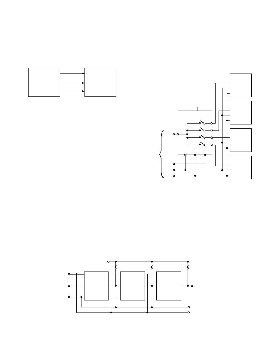
MICROPROCESSOR INTERFACING
Microprocessor interfacing to the ADG738/ADG739 is via a
serial bus that uses standard protocol compatible with micro-
controllers and DSP processors. The communications channel
is a 3-wire (minimum) interface consisting of a clock signal, a data
signal, and a synchronization signal. The ADG738/ADG739 requires
an 8-bit data word with data valid on the falling edge of SCLK.
Data from the previous write cycle is available on the DOUT
pin. The following figures illustrate simple 3-wire interfaces
with popular microcontrollers and DSPs.
ADSP-21xx to ADG738/ADG739
An interface between the ADG738/ADG739 and the ADSP-
21xx is shown in Figure 16. In the interface example shown,
SPORT0 is used to transfer data to the Matrix Switch. The
SPORT control register should be configured as follows: internal
Clock operation, alternate framing mode; active low framing signal.
Transmission is initiated by writing a word to the Tx register
after the SPORT has been enabled. As the data is clocked out of
the DSP on the rising edge of SCLK, no glue logic is required
to interface the DSP to the Matrix Switch. The update of each
switch condition takes place automatically when
TFS is taken high.
SCLK
DIN
SYNC
TFS
DT
SCLK
ADSP-21xx*
*ADDITIONAL PINS OMITTED FOR CLARITY.
ADG738/
ADG739
Figure 16. ADSP-21xx to ADG738/ADG739 Interface
8051 Interface to ADG738/ADG739
A serial interface between the ADG738/ADG739 and the 8051
is shown in Figure 17. TXD of the 8051 drives SCLK of the
ADG738/ADG739, while RXD drives the serial data line, DIN.
P3.3 is a bit-programmable pin on the serial port and is used to
drive
SYNC.
The 8051 provides the LSB of its SBUF register as the first bit
in the data stream. The user will have to ensure that the data in
the SBUF register is arranged correctly as the switch expects
MSB first.
When data is to be transmitted to the Matrix Switch, P3.3 is
taken low. Data on RXD is clocked out of the microcontroller
on the rising edge of TXD and is valid on the falling edge. As a
result no glue logic is required between the ADG738/ADG739
and microcontroller interface.
SCLK
DIN
SYNC
P3.3
RXD
TXD
80C51/80L51*
*ADDITIONAL PINS OMITTED FOR CLARITY.
ADG738/
ADG739
Figure 17. 8051 Interface to ADG738/ADG739
10
REV. 0
ADG738/ADG739
SCLK
DIN
DOUT
ADG739
SCLK
DIN
ADG739
SCLK
DIN
DOUT
DOUT
SCLK
DIN
SYNC
TO OTHER
SERIAL DEVICES
ADG739
V
DD
R
SYNC
SYNC
SYNC
R
R
Figure 20. Multiple ADG739 Devices in a Daisy-Chained Configuration
MC68HC11 Interface to ADG738/ADG739
Figure 18 shows an example of a serial interface between the
ADG738/ADG739 and the MC68HC11 microcontroller. SCK
of the 68HC11 drives the SCLK of the Matrix Switch, while the
MOSI output drives the serial data line, DIN.
SYNC is driven
from one of the port lines, in this case PC7.
SCLK
DIN
SYNC
PC7
MOSI
SCK
MC68HC11*
*ADDITIONAL PINS OMITTED FOR CLARITY.
ADG738/
ADG739
Figure 18. MC68HC11 Interface to ADG738/ADG739
The 68HC11 is configured for master mode; MSTR = 1, CPOL
= 0 and CPHA = 1. When data is transferred to the part, PC7 is
taken low, data is transmitted MSB first. Data appearing on the
MOSI output is valid on the falling edge of SCK.
If the user wishes to verify the data previously written to the input
shift register, the DOUT line could be connected to MISO of
the MC68HC11, and with
SYNC low, the shift register would
clock data out on the rising edges of SCLK.
APPLICATIONS
Expand the Number of Selectable Serial Devices Using an
ADG739
The dual 4-channel ADG739 multiplexer can be used to multiplex
a single chip select line in order to provide chip selects for up to
four devices on the SPI bus. Figure 19 illustrates the ADG739 in
such a typical configuration. All devices receive the same serial
clock and serial data, but only one device will receive the
SYNC signal at any one time. The ADG739 is a serially controlled
device also. One bit programmable pin of the microcontroller is
used to enable the ADG739 via
SYNC2, while another bit
programmable pin is used as the chip select for the other serial
devices,
SYNC1. Driving SYNC2 low enables changes to be
made to the addressed serial devices. By bringing
SYNC1 low,
the selected serial device hanging from the SPI bus will be enabled
and data will be clocked into its shift register on the falling
edges of SCLK. The convenient design of the matrix switch
allows for different combinations of the four serial devices to
be addressed at any one time. If more devices need to be addressed
via one chip select line, the ADG738 is an 8-channel device and
would allow further expansion of the chip select scheme. There
may be some digital feedthrough from the digital input lines
because SCLK and DIN are permanently connected to each
device. Using a burst clock will minimize the effects of digital
feedthrough on the analog channels.
DA
1/2 OF ADG739
V
DD
SCLK
DIN
SYNC
S1A
S2A
S3A
S4A
SYNC1
DIN
SCLK
SYNC
DIN
SCLK
SYNC
DIN
SCLK
SYNC
DIN
SCLK
DIN
SCLK
ADG739
SYNC
ADG738
OTHER SPI
DEVICE
SYNC2
FROM
CONTROLLER
OR DSP
OTHER SPI
DEVICE
Figure 19. Addressing Multiple Serial Devices Using an
ADG739
Daisy-Chaining Multiple ADG738s
A number of ADG738 matrix switches may be daisy-chained
simply by using the DOUT pin. DOUT is an open drain output
that should be pulled to the supply with an external resistor.
Figure 20 shows a typical implementation. The
SYNC pin of all
three parts in the example are tied together. When
SYNC is
brought low, the input shift registers of all parts are enabled,
data is written to the parts via DIN, and clocked through the
shift registers. When the transfer is complete,
SYNC is brought
high and all switches are updated simultaneously. Further shift
registers may be added in series.
ADG738/ADG739
11
REV. 0
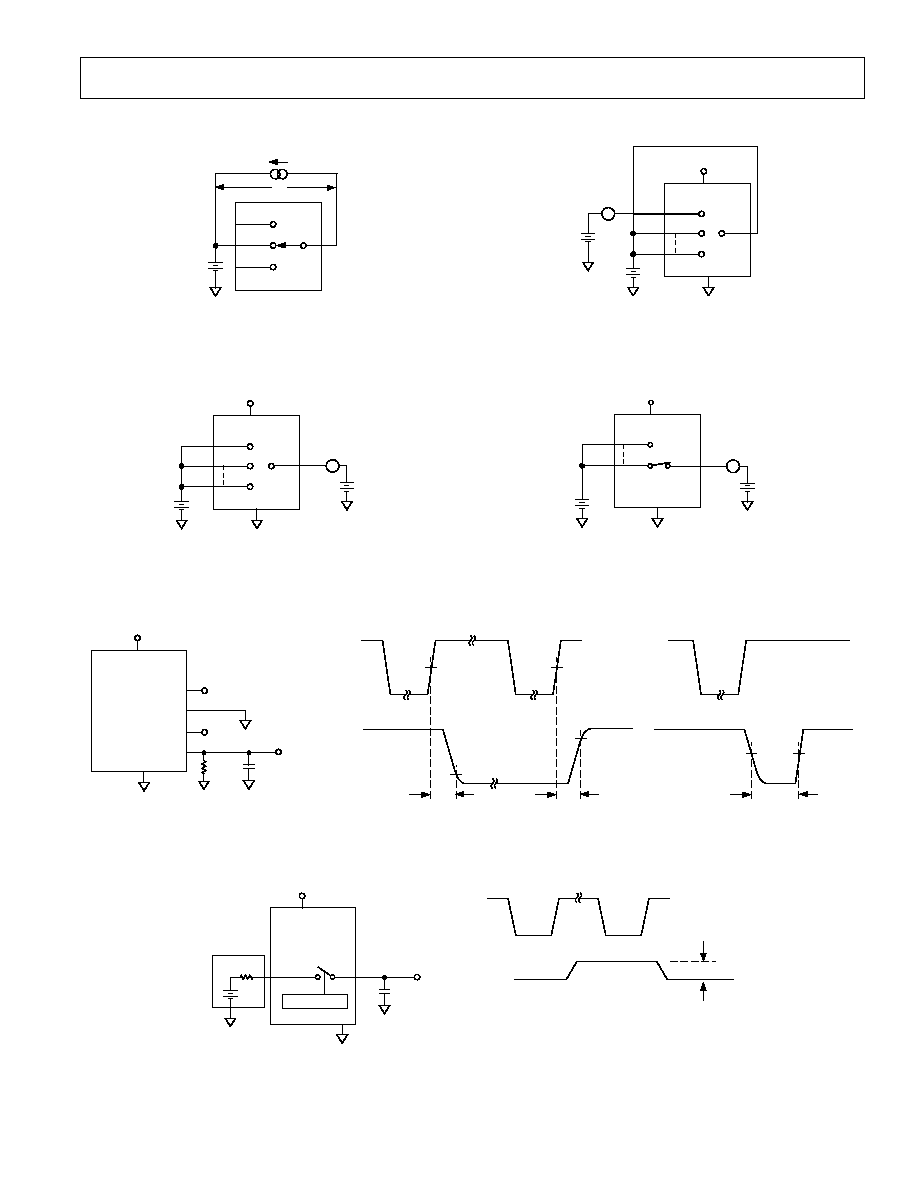
TEST CIRCUITS
I
DS
S
V
S
D
V
1
R
ON
= V
1
/I
DS
Test Circuit 1. On Resistance
S1
S2
S8
D
GND
V
DD
V
DD
V
S
A
I
D
(OFF)
V
D
Test Circuit 2. I
D
(OFF)
I
S
(OFF)
S1
S2
S8
D
A
GND
V
DD
V
DD
V
D
V
S
Test Circuit 3. I
S
(OFF)
S1
S8
D
GND
V
DD
V
DD
V
S
A
I
D
(ON)
V
D
Test Circuit 4. I
D
(ON)
GND
V
DD
V
DD
50%
t
OFF
90%
90%
50%
V
OUT
D
V
S1
ADG738*
S1
S8
S2 THRU S7
R
L
300
C
L
35pF
SYNC
V
S1
80%
80%
V
S1
= V
S8
V
S8
V
OUT
V
OUT
SYNC
t
ON
t
OPEN
* SIMILAR CONNECTION FOR ADG739
Test Circuit 5. Switching Times and Break-Before-Make Times
GND
V
DD
ADG738*
1nF
INPUT LOGIC
V
OUT
C
L
V
S
R
S
D
* SIMILAR CONNECTION FOR ADG739
S
SYNC
SWITCH OFF
SWITCH ON
V
OUT
Q
INJ
= C
L
x V
OUT
Test Circuit 6. Charge Injection

ADG738/ADG739
12
REV .0
PRIN
TED IN U
.S.A.
C383484/0
0 (rev
. 0) 0
1
0
0
3
OUTLINE DIMENSIONS
Dimensions shown in inches and (mm).
16-Lead TSSOP
(RU-16)
16
9
8
1
0.256 (6.50)
0.246 (6.25)
0.177 (4.50)
0.169 (4.30)
PIN 1
0.201 (5.10)
0.193 (4.90)
SEATING
PLANE
0.006 (0.15)
0.002 (0.05)
0.0118 (0.30)
0.0075 (0.19)
0.0256 (0.65)
BSC
0.0433 (1.10)
MAX
0.0079 (0.20)
0.0035 (0.090)
0.028 (0.70)
0.020 (0.50)
8
0
GND
ADG738*
S1
S2
S8
* SIMILAR CONNECTION FOR ADG739
CHANNEL-TO-CHANNEL CROSSTALK = 20LOG
10
(V
OUT
/V
S
)
V
OUT
V
DD
R
L
50
V
DD
50
V
S
D
Test Circuit 7. Channel-to-Channel Crosstalk
GND
ADG738*
50
S1
S8
V
OUT
V
DD
R
L
V
DD
V
S
D
*SIMILAR CONNECTION FOR ADG739
OFF ISOLATION = 20LOG
10
(V
OUT
/V
S
)
V
OUT
WITHOUT SWITCH
INSERTION LOSS = 20LOG
10
V
OUT
WITH SWITCH
S1 IS SWITCHED OFF FOR OFF ISOLATION MEASUREMENTS
AND ON FOR BANDWIDTH MEASUREMENTS
Test Circuit 8. Off Isolation and Bandwidth