 | ÐлекÑÑоннÑй компоненÑ: ADG752BRT | СкаÑаÑÑ:  PDF PDF  ZIP ZIP |
Äîêóìåíòàöèÿ è îïèñàíèÿ www.docs.chipfind.ru
REV. 0
Information furnished by Analog Devices is believed to be accurate and
reliable. However, no responsibility is assumed by Analog Devices for its
use, nor for any infringements of patents or other rights of third parties
which may result from its use. No license is granted by implication or
otherwise under any patent or patent rights of Analog Devices.
a
ADG752
One Technology Way, P.O. Box 9106, Norwood, MA 02062-9106, U.S.A.
Tel: 781/329-4700
World Wide Web Site: http://www.analog.com
Fax: 781/326-8703
© Analog Devices, Inc., 1999
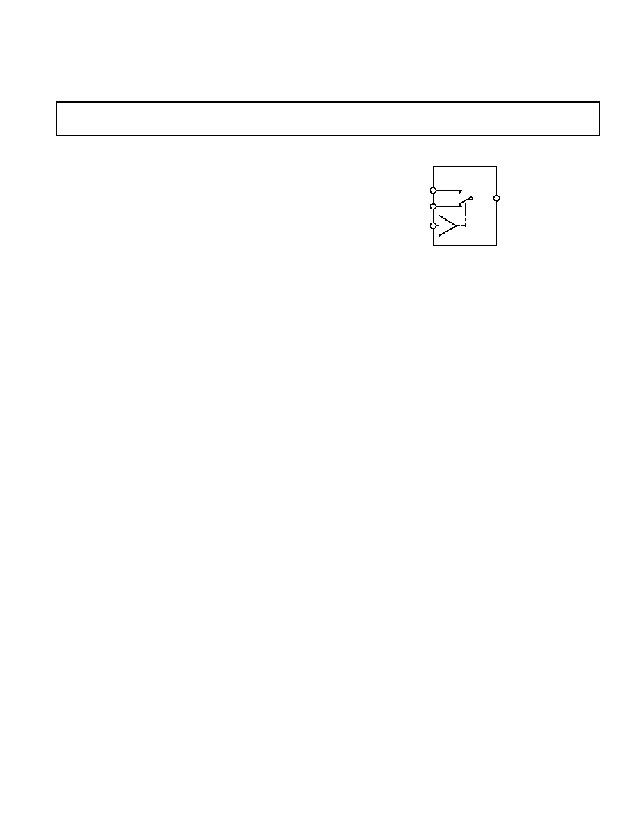
FUNCTIONAL BLOCK DIAGRAM
CMOS, Low Voltage
RF/Video, SPDT Switch
IN
D
S2
S1
ADG752
SWITCH SHOWN FOR A LOGIC "1" INPUT
FEATURES
High Off Isolation 80 dB at 30 MHz
3 dB Signal Bandwidth 250 MHz
+1.8 V to +5.5 V Single Supply
Low On-Resistance (15
Typically)
Low On-Resistance Flatness
Fast Switching Times
t
ON
Typically 8 ns
t
OFF
Typically 3 ns
Typical Power Consumption < 0.01 W
TTL/CMOS Compatible
APPLICATIONS
Audio and Video Switching
RF Switching
Networking Applications
Battery Powered Systems
Communication Systems
Relay Replacement
Sample-and-Hold Systems
GENERAL DESCRIPTION
The ADG752 is a low voltage SPDT (single pole, double throw)
switch. It is constructed using switches in a T-switch configura-
tion, which results in excellent Off Isolation while maintaining
good frequency response in the ON condition.
High off isolation and wide signal bandwidth make this part
suitable for switching RF and video signals. Low power con-
sumption and operating supply range of +1.8 V to +5.5 V make
it ideal for battery powered, portable instruments.
The ADG752 is designed on a submicron process that provides
low power dissipation yet gives high switching speed and low on
resistance. This part is a fully bidirectional switch and can handle
signals up to and including the supply rails. Break-before-make
switching action ensures the input signals are protected against
momentary shorting when switching between channels.
The ADG752 is available in 6-lead SOT-23 and 8-lead
µ
SOIC
packages.
PRODUCT HIGHLIGHTS
1. High Off Isolation 80 dB at 30 MHz.
2. 3 dB Signal Bandwidth 250 MHz.
3. Low On Resistance (15
).
4. Low Power Consumption, typically <0.01
µ
W.
5. Break-Before-Make Switching Action.
6. Tiny 6-lead SOT-23 and 8-lead
µ
SOIC packages.

REV. 0
2
ADG752SPECIFICATIONS
(V
DD
= +5 V
10%, GND = 0 V, unless otherwise noted.)
B Version
40 C
Parameter
+25 C
to +85 C
Units
Test Conditions/Comments
ANALOG SWITCH
Analog Signal Range
0 V to V
DD
V
On-Resistance (R
ON
)
15
typ
V
S
= 0 V to V
DD
, I
DS
= 10 mA;
18
20
max
Test Circuit 1
On-Resistance Match Between
0.1
typ
V
S
= 0 V to V
DD
, I
DS
= 10 mA
Channels (
R
ON
)
0.6
0.6
max
On-Resistance Flatness (R
FLAT(ON)
)
2
typ
V
S
= 0 V to 2.5 V, I
DS
= 10 mA
3
max
V
DD
= + 4.5 V
LEAKAGE CURRENTS
Source OFF Leakage I
S
(OFF)
±
0.01
nA typ
V
D
= 4.5 V/1 V, V
S
= 1 V/4.5 V;
±
0.25
±
3.0
nA max
Test Circuit 2
Channel ON Leakage I
D
, I
S
(ON)
±
0.01
nA typ
V
D
= V
S
= 1 V, or 4.5 V;
±
0.25
±
3.0
nA max
Test Circuit 3
DIGITAL INPUTS
Input High Voltage, V
INH
2.4
V min
Input Low Voltage, V
INL
0.8
V max
Input Current
I
INL
or I
INH
0.001
µ
A typ
V
IN
= V
INL
or V
INH
±
0.5
µ
A max
C
IN
, Digital Input Capacitance
2
pF typ
DYNAMIC CHARACTERISTICS
1
t
ON
8
ns typ
R
L
= 300
, C
L
= 35 pF;
13
ns max
V
S
= 3 V, Test Circuit 4
t
OFF
3
ns typ
R
L
= 300
, C
L
= 35 pF;
5
ns max
V
S
= 3 V, Test Circuit 4
Break-Before-Make Time Delay
6
ns typ
R
L
= 300
, C
L
= 35 pF;
1
ns min
V
S
= 3 V, Test Circuit 5
Off Isolation
80
dB typ
R
L
= 50
, C
L
= 5 pF, f = 30 MHz;
Test Circuit 6
Crosstalk
80
dB typ
R
L
= 50
, C
L
= 5 pF, f = 30 MHz;
Test Circuit 7
3 dB Bandwidth
250
MHz typ
R
L
= 50
, C
L
= 5 pF, Test Circuit 8
C
S
(OFF)
4
pF typ
C
D
, C
S
(ON)
15
pF typ
POWER REQUIREMENTS
V
DD
= +5.5 V
I
DD
0.001
µ
A typ
Digital Inputs = 0 V or +5.5 V
0.1
0.5
µ
A max
NOTES
1
Guaranteed by design, not subject to production test.
Specifications subject to change without notice.

REV. 0
3
ADG752
(V
DD
= +3 V
10%, GND = 0 V, unless otherwise noted.)
B Version
40 C
Parameter
+25 C
to +85 C
Units
Test Conditions/Comments
ANALOG SWITCH
Analog Signal Range
0 V to V
DD
V
On-Resistance (R
ON
)
35
typ
V
S
= 0 V to V
DD
, I
DS
= 10 mA;
50
max
Test Circuit 1
On-Resistance Match Between
0.2
typ
V
S
= 0 V to V
DD
, I
DS
= 10 mA
Channels (
R
ON
)
2.5
2.5
max
LEAKAGE CURRENTS
V
DD
= +3.3 V
Source OFF Leakage I
S
(OFF)
±
0.01
nA typ
V
S
= 3 V/1 V, V
D
= 1 V/3 V;
±
0.25
±
3.0
nA max
Test Circuit 2
Channel ON Leakage I
D
, I
S
(ON)
±
0.01
nA typ
V
S
= V
D
= 1 V or 3 V;
±
0.25
±
3.0
nA max
Test Circuit 3
DIGITAL INPUTS
Input High Voltage, V
INH
2.0
V min
Input Low Voltage, V
INL
0.4
V max
Input Current
I
INL
or I
INH
0.001
µ
A typ
V
IN
= V
INL
or V
INH
±
0.5
µ
A max
C
IN
, Digital Input Capacitance
2
pF typ
DYNAMIC CHARACTERISTICS
1
t
ON
10
ns typ
R
L
= 300
, C
L
= 35 pF;
18
ns max
V
S
= 2 V, Test Circuit 4
t
OFF
4
ns typ
R
L
= 300
, C
L
= 35 pF;
8
ns max
V
S
= 2 V, Test Circuit 4
Break-Before-Make Time Delay
6
ns typ
R
L
= 300
, C
L
= 35 pF;
1
ns min
V
S
= 2 V, Test Circuit 5
Off Isolation
80
dB typ
R
L
= 50
, C
L
= 5 pF, f = 30 MHz;
Test Circuit 6
Crosstalk
80
dB typ
R
L
= 50
, C
L
= 5 pF, f = 30 MHz;
Test Circuit 7
3 dB Bandwidth
250
MHz typ
R
L
= 50
, C
L
= 5 pF, Test Circuit 8
C
S
(OFF)
4
pF typ
C
D
, C
S
(ON)
15
pF typ
POWER REQUIREMENTS
V
DD
= +3.3 V
I
DD
0.001
µ
A typ
Digital Inputs = 0 V or +3.3 V
0.1
0.5
µ
A max
NOTES
1
Guaranteed by design, not subject to production test.
Specifications subject to change without notice.
SPECIFICATIONS
REV. 0
ADG752
4
Table I. Truth Table
ADG752 IN
Switch S1
Switch S2
0
ON
OFF
1
OFF
ON
CAUTION
ESD (electrostatic discharge) sensitive device. Electrostatic charges as high as 4000 V readily
accumulate on the human body and test equipment and can discharge without detection.
Although the ADG752 features proprietary ESD protection circuitry, permanent damage may
occur on devices subjected to high energy electrostatic discharges. Therefore, proper ESD
precautions are recommended to avoid performance degradation or loss of functionality.
WARNING!
ESD SENSITIVE DEVICE
ABSOLUTE MAXIMUM RATINGS
1
(T
A
= +25
°
C unless otherwise noted)
V
DD
to GND . . . . . . . . . . . . . . . . . . . . . . . . . . . 0.3 V to +6 V
Analog, Digital Inputs
2
. . . . . . . . . . . . 0.3 V to V
DD
+0.3 V or
30 mA, Whichever Occurs First
Peak Current, S or D . . . . . . . . . . . . . . . . . . . . . . . . . . .100 mA
(Pulsed at 1 ms, 10% Duty Cycle Max)
Continuous Current, S or D . . . . . . . . . . . . . . . . . . . . . 30 mA
Operating Temperature Range
Industrial (B Version) . . . . . . . . . . . . . . . . . 40
°
C to +85
°
C
Storage Temperature Range . . . . . . . . . . . . . 65
°
C to +150
°
C
Power Dissipation . . . . . . . . . . . . . . . . . . . . . (T
J
MaxT
A
)/
JA
Junction Temperature (T
J
Max) . . . . . . . . . . . . . . . . . .+150
°
C
µ
SOIC Package
JA
Thermal Impedance . . . . . . . . . . . . . . . . . . . . . 206
°
C/W
JC
Thermal Impedance . . . . . . . . . . . . . . . . . . . . . . 44
°
C/W
SOT-23 Package
JA
Thermal Impedance . . . . . . . . . . . . . . . . . . . . 229.6
°
C/W
JC
Thermal Impedance . . . . . . . . . . . . . . . . . . . . 91.99
°
C/W
Lead Temperature, Soldering
Vapor Phase (60 sec) . . . . . . . . . . . . . . . . . . . . . . . . . +215
°
C
Infrared (15 sec) . . . . . . . . . . . . . . . . . . . . . . . . . . . . .+220
°
C
NOTES
1
Stresses above those listed under Absolute Maximum Ratings may cause perma-
nent damage to the device. This is a stress rating only; functional operation of the
device at these or any other conditions above those listed in the operational sections
of this specification is not implied. Exposure to absolute maximum rating condi-
tions for extended periods may affect device reliability. Only one absolute maxi-
mum rating may be applied at any one time.
2
Overvoltages at IN, S or D will be clamped by internal diodes. Current should be
limited to the maximum ratings given.
ORDERING GUIDE
Model
Temperature Range
Brand*
Package Descriptions
Package Options
ADG752BRM
40
°
C to +85
°
C
SEB
µ
SOIC
RM-8
ADG752BRT
40
°
C to +85
°
C
SEB
SOT-23
RT-6
*Brand on these packages is limited to three characters due to space constraints.
TERMINOLOGY
V
DD
Most positive power supply potential.
GND
Ground (0 V) reference.
S
Source terminal. May be an input or output.
D
Drain terminal. May be an input or output.
IN
Logic control input.
R
ON
Ohmic resistance between D and S.
R
ON
On resistance match between channels, i.e.,
R
ON
maxR
ON
min.
R
FLAT(ON)
Flatness is defined as the difference between
the maximum and minimum value of on resis-
tance as measured over the specified analog
signal range.
I
S
(OFF)
Source leakage current with the switch "OFF."
I
D
, I
S
(ON)
Channel leakage current with the switch "ON."
V
D
(V
S
)
Analog voltage on terminals D and S.
C
S
(OFF)
"OFF" switch source capacitance.
C
D
, C
S
(ON)
"ON" switch capacitance.
t
ON
Delay between applying the digital control
input and the output switching on. See Test
Circuit 4.
t
OFF
Delay between applying the digital control
input and the output switching off.
t
D
"OFF" time or "ON" time measured between
the 90% points of both switches, when switch-
ing from one address state to another.
Off Isolation
A measure of unwanted signal coupling
through an "OFF" switch.
Crosstalk
A measure of unwanted signal that is coupled
through from one channel to another as a
result of parasitic capacitance.
Bandwidth
The frequency at which the output is attenu-
ated by 3 dBs.
On Response
The frequency response of the "ON" switch.
Insertion Loss
Loss due to the ON resistance of the switch.
V
INL
Maximum input voltage for Logic "0."
V
INH
Minimum input voltage for Logic "1."
I
INL
(I
INH
)
Input current of the digital input.
I
DD
Positive supply current.
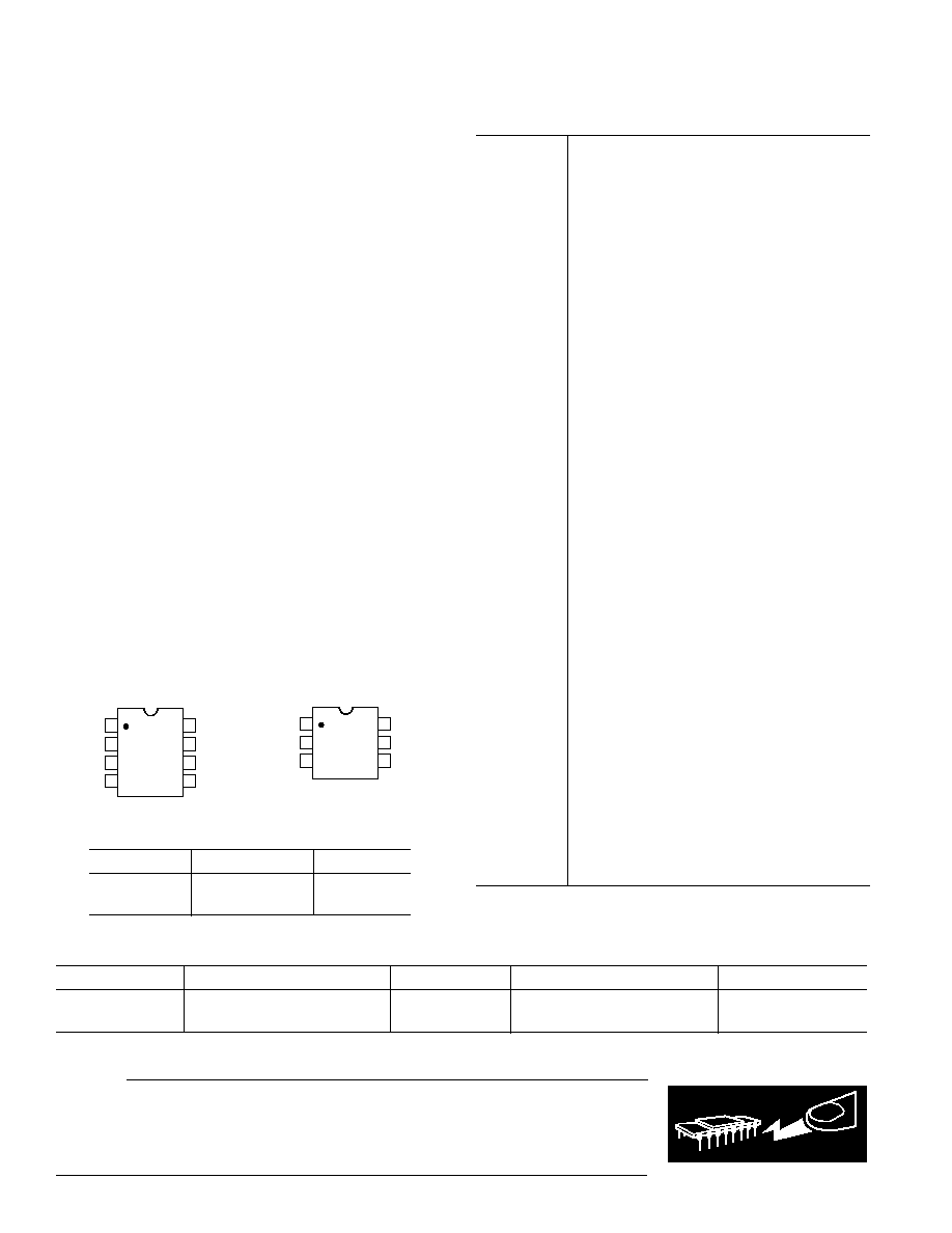
PIN CONFIGURATIONS
6-Lead SOT-23
(RT-6)
1
2
3
6
5
4
TOP VIEW
(Not to Scale)
ADG752
IN
D
V
DD
S1
GND
S2
8-Lead SOIC
(RM-8)
1
2
3
4
8
7
6
5
TOP VIEW
(Not to Scale)
NC = NO CONNECT
ADG752
NC
NC
S1
D
V
DD
S2
GND
IN
REV. 0
ADG752
5
V
D
OR V
S
DRAIN SOURCE VOLTAGE Volts
35
5
0
1
R
ON
2
3
4
5
30
25
20
15
10
V
DD
= +5.5V
T
A
= +25 C
V
DD
= +2.7V
V
DD
= +3.3V
V
DD
= +4.5V
40
5.5
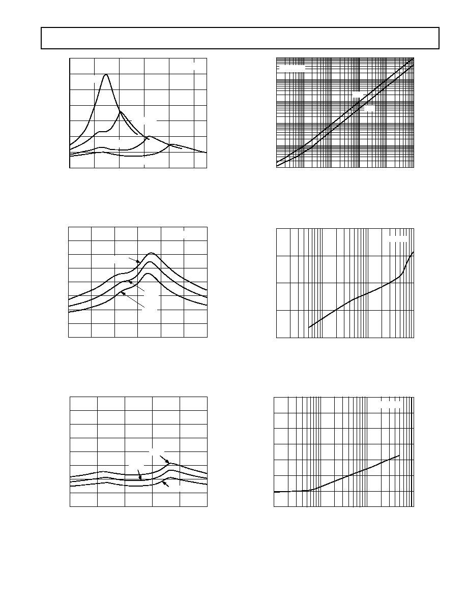
Figure 1. On Resistance as a Function of V
D
(V
S
) Single
Supplies
V
D
OR V
S
DRAIN SOURCE VOLTAGE Volts
40
0
0
0.5
R
ON
1.0
1.5
2.0
2.5
35
30
25
20
15
40 C
3.0
+25 C
+85 C
V
DD
= +3V
10
5
Figure 2. On Resistance as a Function of V
D
(V
S
) for
Different Temperatures V
DD
= 3 V
V
D
OR V
S
DRAIN SOURCE VOLTAGE Volts
40
10
0
1
R
ON
2
3
35
30
25
20
15
5
+25 C
V
DD
= +5V
4
0
5
40 C
+85 C
Figure 3. On Resistance as a Function of V
D
(V
S
) for
Different Temperatures V
DD
= 5 V
FREQUENCY Hz
10n
100
I
DD
Amps
1k
10k
100n
10
1
1m
10m
100k
100M
10M
+5V
+3V
T
A
= +25 C
Figure 4. Supply Current vs. Input Switching Frequency
FREQUENCY MHz
120
0.1
100
OFF ISOLATION dB
10
1
100
80
60
40
T
A
= +25°C
Figure 5. Off Isolation vs. Frequency
FREQUENCY MHz
80
CROSSTALK dB
60
40
20
0
0.1
1
10
100
140
120
100
T
A
= +25 C
Figure 6. Crosstalk vs. Frequency
Typical Performance Characteristics
REV. 0
ADG752
6
FREQUENCY MHz
100
ATTENUATION dB
10
1
8
4
2
0
6
T
A
= +25 C
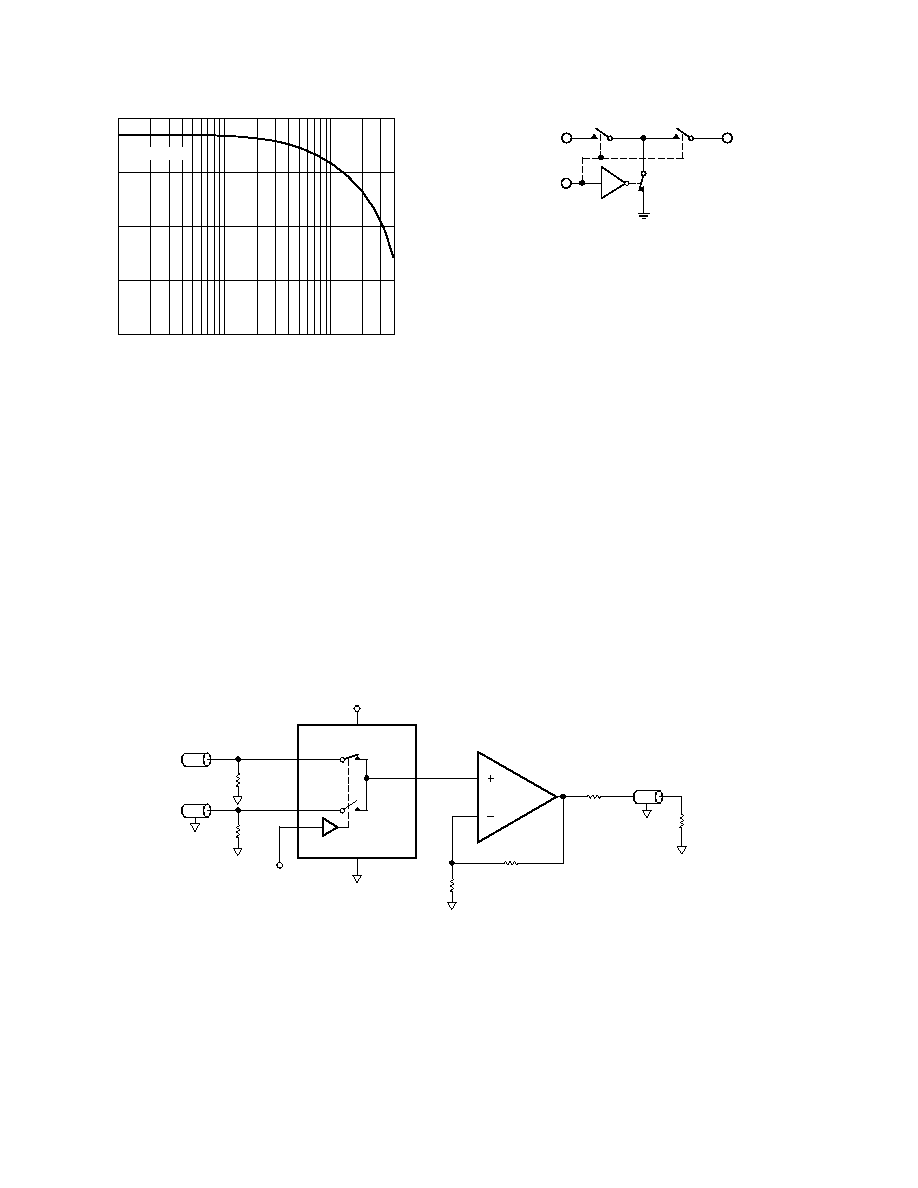
Figure 7. On Response vs. Frequency
GENERAL DESCRIPTION
The ADG752 is an SPDT switch constructed using switches in
a T configuration to obtain high "OFF" isolation while main-
taining good frequency response in the "ON" condition.
Figure 8 shows the T-switch configuration. While the switch is
in the OFF state, the shunt switch is closed and the two series
switches are open. The closed shunt switch provides a signal
path to ground for any of the unwanted signals that find their
way through the off capacitances of the series' MOS devices.
This results in more improved isolation between the input and
output than with an ordinary series switch. When the switch is
in the ON condition, the shunt switch is open and the signal
path is through the two series switches which are now closed.
D
IN
S
SERIES
SHUNT
Figure 8. Basic T-Switch Configuration
LAYOUT CONSIDERATIONS
Where accurate high frequency operation is important, careful
consideration should be given to the printed circuit board layout
and to grounding. Wire wrap boards, prototype boards and
sockets are not recommended because of their high parasitic
inductance and capacitance. The part should be soldered di-
rectly to a printed circuit board. A ground plane should cover all
unused areas of the component side of the board to provide a
low impedance path to ground. Removing the ground planes
from the area around the part reduces stray capacitance.
Good decoupling is important in achieving optimum perfor-
mance. V
DD
should be decoupled with a 0.1
µ
F surface mount
capacitor to ground mounted as close as possible to the device
itself.
V
DD
IN
ADG752
D
S1
S2
75
V
OUT
75
CH1
CH2
A
=
2
250
250
75
75
Figure 9. Multiplexing Between Two Video Signals
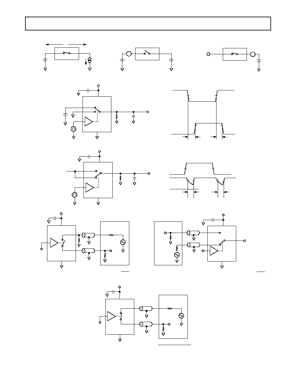
REV. 0
ADG752
7
V
S
V
OUT
50
NETWORK
ANALYZER
R
L
50
IN
GND
V
DD
V
DD
V
IN
S
0.1 F
D
INSERTION
LOSS
=
20
LOG
V
OUT
WITH
SWITCH
V
OUT
WITHOUT
SWITCH
Test Circuit 8. Bandwidth
S
D
V
S
R
ON
= V1/I
DS
I
DS
V1
Test Circuit 1. On Resistance
S
D
V
S
A
V
D
I
S
(OFF)
Test Circuit 2. Off Leakage
S
D
A
V
D
I
D
(ON)
NC
NC = NO CONNECT
Test Circuit 3. On Leakage
Test Circuits
CHANNEL-TO-CHANNEL
CROSSTALK = 20
LOG
GND
V
DD
0.1 F
V
DD
S1
D
S2
V
S
V
OUT
NETWORK
ANALYZER
R
L
50
IN
V
OUT
V
S
50
Test Circuit 7. Channel-to-Channel Crosstalk
V
S
V
OUT
50
NETWORK
ANALYZER
R
L
50
IN
GND
V
DD
V
DD
V
IN
S
0.1 F
D
50
OFF
ISOLATION
=
20
LOG
V
OUT
V
S
Test Circuit 6. Off Isolation
50%
50%
50%
50%
t
D
t
D
0V
0V
V
OUT
V
IN
IN
GND
R
L
300
C
L
35pF
V
OUT
V
DD
0.1 F
V
DD
S1
D
S2
V
S
D2
V
IN
Test Circuit 5. Break-Before-Make Time Delay, t
D
V
S
IN
GND
R
L
300
C
L
35pF
V
OUT
V
DD
0.1 F
V
DD
S1
D
S2
90%
90%
50%
50%
V
IN
V
OUT
t
OFF
t
ON
GND
V
S
Test Circuit 4. Switching Times
REV. 0
ADG752
8
OUTLINE DIMENSIONS
Dimensions shown in inches and (mm).
C356884/99
PRINTED IN U.S.A.
8-Lead SOIC
(RM-8)
0.011 (0.28)
0.003 (0.08)
0.028 (0.71)
0.016 (0.41)
33
27
0.120 (3.05)
0.112 (2.84)
8
5
4
1
0.122 (3.10)
0.114 (2.90)
0.199 (5.05)
0.187 (4.75)
PIN 1
0.0256 (0.65) BSC
0.122 (3.10)
0.114 (2.90)
SEATING
PLANE
0.006 (0.15)
0.002 (0.05)
0.018 (0.46)
0.008 (0.20)
0.043 (1.09)
0.037 (0.94)
0.120 (3.05)
0.112 (2.84)
6-Lead SOT-23
(RT-6)
0.122 (3.10)
0.106 (2.70)
PIN 1
0.118 (3.00)
0.098 (2.50)
0.075 (1.90)
BSC
0.037 (0.95) BSC
1
3
4
5
6
2
0.071 (1.80)
0.059 (1.50)
0.009 (0.23)
0.003 (0.08)
0.022 (0.55)
0.014 (0.35)
10
0
0.020 (0.50)
0.010 (0.25)
0.006 (0.15)
0.000 (0.00)
0.051 (1.30)
0.035 (0.90)
SEATING
PLANE
0.057 (1.45)
0.035 (0.90)