 | ÐлекÑÑоннÑй компоненÑ: ADG759 | СкаÑаÑÑ:  PDF PDF  ZIP ZIP |
Äîêóìåíòàöèÿ è îïèñàíèÿ www.docs.chipfind.ru
REV. A
Information furnished by Analog Devices is believed to be accurate and
reliable. However, no responsibility is assumed by Analog Devices for its
use, nor for any infringements of patents or other rights of third parties that
may result from its use. No license is granted by implication or otherwise
under any patent or patent rights of Analog Devices.
a
ADG758/ADG759
One Technology Way, P.O. Box 9106, Norwood, MA 02062-9106, U.S.A.
Tel: 781/329-4700
www.analog.com
Fax: 781/326-8703
© Analog Devices, Inc., 2002
3 ,
4-/8-Channel Multiplexers
in Chip Scale Package
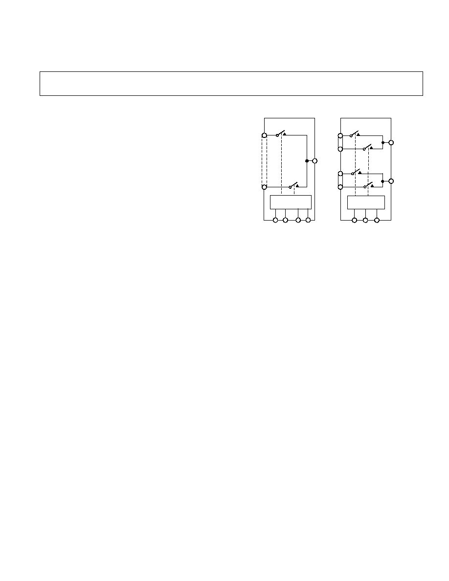
FUNCTIONAL BLOCK DIAGRAMS
S1
S8
A0
D
A1
A2
ADG758
S1A
A0
DA
S4A
S1B
S4B
DB
EN
ADG759
1 OF 4
DECODER
EN
1 OF 8
DECODER
A1
FEATURES
1.8 V to 5.5 V Single Supply
2.5 V Dual Supply
3 ON Resistance
0.75 ON Resistance Flatness
100 pA Leakage Currents
14 ns Switching Times
Single 8-to-1 Multiplexer ADG758
Differential 4-to-1 Multiplexer ADG759
20-Lead 4 mm 4 mm Chip Scale Package
Low Power Consumption
TTL-/CMOS-Compatible Inputs
For Functionally Equivalent Devices in 16-Lead TSSOP
Package, See ADG708/ADG709
APPLICATIONS
Data Acquisition Systems
Communication Systems
Relay Replacement
Audio and Video Switching
Battery-Powered Systems
GENERAL DESCRIPTION
The ADG758 and ADG759 are low voltage, CMOS analog
multiplexers comprising eight single channels and four differential
channels, respectively. The ADG758 switches one of eight inputs
(S1S8) to a common output, D, as determined by the 3-bit
binary address lines A0, A1, and A2. The ADG759 switches one
of four differential inputs to a common differential output as
determined by the 2-bit binary address lines A0 and A1. An EN
input on both devices is used to enable or disable the device. When
disabled, all channels are switched OFF.
Low power consumption and an operating supply range of 1.8 V to
5.5 V make the ADG758 and ADG759 ideal for battery-powered,
portable instruments. All channels exhibit break-before-make
switching action preventing momentary shorting when switch-
ing channels.
These switches are designed on an enhanced submicron process
that provides low power dissipation yet gives high switching
speed, very low ON resistance and leakage currents. ON resistance
is in the region of a few ohms and is closely matched between
switches and very flat over the full signal range. These parts can
operate equally well as either multiplexers or demultiplexers
and have an input signal range that extends to the supplies.
The ADG758 and ADG759 are available in 20-lead chip
scale packages.
PRODUCT HIGHLIGHTS
1. Small 20-Lead 4 mm
× 4 mm Chip Scale Packages (CSP).
2. Single/Dual Supply Operation. The ADG758 and ADG759
are fully specified and guaranteed with 3 V and 5 V single-
supply and
±2.5 V dual-supply rails.
3. Low R
ON
(3
Typical).
4. Low Power Consumption (<0.01
µW).
5. Guaranteed Break-Before-Make Switching Action.

2
REV. A
ADG758/ADG759SPECIFICATIONS
1
(V
DD
= 5 V 10%, V
SS
= 0 V, GND = 0 V, unless otherwise noted.)
B Version
40 C
Parameter
+25 C
to +85 C
Unit
Test Conditions/Comments
ANALOG SWITCH
Analog Signal Range
0 V to V
DD
V
ON Resistance (R
ON
)
3
typ
V
S
= 0 V to V
DD
, I
DS
= 10 mA;
4.5
5
max
Test Circuit 1
ON Resistance Match Between
0.4
typ
Channels (
R
ON
)
0.8
max
V
S
= 0 V to V
DD
, I
DS
= 10 mA
ON Resistance Flatness (R
FLAT(ON)
)
0.75
typ
V
S
= 0 V to V
DD
, I
DS
= 10 mA
1.2
max
LEAKAGE CURRENTS
V
DD
= 5.5 V
Source OFF Leakage I
S
(OFF)
±0.01
nA typ
V
D
= 4.5 V/1 V, V
S
= 1 V/4.5 V;
±0.1
±0.3
nA max
Test Circuit 2
Drain OFF Leakage I
D
(OFF)
±0.01
nA typ
V
D
= 4.5 V/1 V, V
S
= 1 V/4.5 V;
±0.1
±0.75
nA max
Test Circuit 3
Channel ON Leakage I
D
, I
S
(ON)
±0.01
nA typ
V
D
= V
S
= 1 V, or 4.5 V, Test Circuit 4
±0.1
±0.75
nA max
DIGITAL INPUTS
Input High Voltage, V
INH
2.4
V min
Input Low Voltage, V
INL
0.8
V max
Input Current
I
INL
or I
INH
0.005
µA typ
V
IN
= V
INL
or V
INH
±0.1
µA max
C
IN
, Digital Input Capacitance
2
pF typ
DYNAMIC CHARACTERISTICS
2
t
TRANSITION
14
ns typ
R
L
= 300
, C
L
= 35 pF; Test Circuit 5
25
ns max
V
S1
= 3 V/0 V, V
S8
= 0 V/3 V
Break-Before-Make Time Delay, t
D
8
ns typ
R
L
= 300
, C
L
= 35 pF
1
ns min
V
S
= 3 V; Test Circuit 6
t
ON
(EN)
14
ns typ
R
L
= 300
, C
L
= 35 pF
25
ns max
V
S
= 3 V; Test Circuit 7
t
OFF
(EN)
7
ns typ
R
L
= 300
, C
L
= 35 pF
12
ns max
V
S
= 3 V; Test Circuit 7
Charge Injection
±3
pC typ
V
S
= 2.5 V, R
S
= 0
, C
L
= 1 nF;
Test Circuit 8
Off Isolation
60
dB typ
R
L
= 50
, C
L
= 5 pF, f = 10 MHz
80
dB typ
R
L
= 50
, C
L
= 5 pF, f = 1 MHz;
Test Circuit 9
Channel-to-Channel Crosstalk
60
dB typ
R
L
= 50
, C
L
= 5 pF, f = 10 MHz
80
dB typ
R
L
= 50
, C
L
= 5 pF, f = 1 MHz;
Test Circuit 10
3 dB Bandwidth
55
MHz typ
R
L
= 50
, C
L
= 5 pF; Test Circuit 11
C
S
(OFF)
13
pF typ
f = 1 MHz
C
D
(OFF)
ADG758
85
pF typ
f = 1 MHz
ADG759
42
pF typ
f = 1 MHz
C
D
, C
S
(ON)
ADG758
96
pF typ
f = 1 MHz
ADG759
48
pF typ
f = 1 MHz
POWER REQUIREMENTS
V
DD
= 5.5 V
I
DD
0.001
µA typ
Digital Inputs = 0 V or 5.5 V
1.0
µA max
NOTES
1
Temperature range is as follows: B Version: 40
°C to +85°C.
2
Guaranteed by design, not subject to production test.
Specifications subject to change without notice.

3
REV. A
ADG758/ADG759
SPECIFICATIONS
1
(V
DD
= 3 V 10%, V
SS
= 0 V, GND = 0 V, unless otherwise noted.)
B Version
40 C
Parameter
+25 C
to +85 C
Unit
Test Conditions/Comments
ANALOG SWITCH
Analog Signal Range
0 V to V
DD
V
ON Resistance (R
ON
)
8
typ
V
S
= 0 V to V
DD
, I
DS
= 10 mA;
11
12
max
Test Circuit 1
ON Resistance Match Between
0.4
typ
V
S
= 0 V to V
DD
, I
DS
= 10 mA
Channels (
R
ON
)
1.2
max
LEAKAGE CURRENTS
V
DD
= 3.3 V
Source OFF Leakage I
S
(OFF)
±0.01
nA typ
V
S
= 3 V/1 V, V
D
= 1 V/3 V;
±0.1
±0.3
nA max
Test Circuit 2
Drain OFF Leakage I
D
(OFF)
±0.01
nA typ
V
S
= 3 V/1 V, V
D
= 1 V/3 V;
±0.1
±0.75
nA max
Test Circuit 3
Channel ON Leakage I
D
, I
S
(ON)
±0.01
nA typ
V
S
= V
D
= 1 V or 3 V; Test Circuit 4
±0.1
±0.75
nA max
DIGITAL INPUTS
Input High Voltage, V
INH
2.0
V min
Input Low Voltage, V
INL
0.8
V max
Input Current
I
INL
or I
INH
0.005
µA typ
V
IN
= V
INL
or V
INH
±0.1
µA max
C
IN
, Digital Input Capacitance
2
pF typ
DYNAMIC CHARACTERISTICS
2
t
TRANSITION
18
ns typ
R
L
= 300
, C
L
= 35 pF; Test Circuit 5
30
ns max
V
S1
= 2 V/0 V, V
S2
= 0 V/2 V
Break-Before-Make Time Delay, t
D
8
ns typ
R
L
= 300
, C
L
= 35 pF
1
ns min
V
S
= 2 V; Test Circuit 6
t
ON
(EN)
18
ns typ
R
L
= 300
, C
L
= 35 pF
30
ns max
V
S
= 2 V; Test Circuit 7
t
OFF
(EN)
8
ns typ
R
L
= 300
, C
L
= 35 pF
15
ns max
V
S
= 2 V; Test Circuit 7
Charge Injection
±3
pC typ
V
S
= 1.5 V, R
S
= 0
, C
L
= 1 nF;
Test Circuit 8
Off Isolation
60
dB typ
R
L
= 50
, C
L
= 5 pF, f = 10 MHz
80
dB typ
R
L
= 50
, C
L
= 5 pF, f = 1 MHz;
Test Circuit 9
Channel-to-Channel Crosstalk
60
dB typ
R
L
= 50
, C
L
= 5 pF, f = 10 MHz
80
dB typ
R
L
= 50
, C
L
= 5 pF, f = 1 MHz;
Test Circuit 10
3 dB Bandwidth
55
MHz typ
R
L
= 50
, C
L
= 5 pF; Test Circuit 11
C
S
(OFF)
13
pF typ
f = 1 MHz
C
D
(OFF)
ADG758
85
pF typ
f = 1 MHz
ADG759
42
pF typ
f = 1 MHz
C
D
, C
S
(ON)
ADG758
96
pF typ
f = 1 MHz
ADG759
48
pF typ
f = 1 MHz
POWER REQUIREMENTS
V
DD
= 3.3 V
I
DD
0.001
µA typ
Digital Inputs = 0 V or 3.3 V
1.0
µA max
NOTES
1
Temperature ranges are as follows: B Version: 40
°C to +85°C.
2
Guaranteed by design, not subject to production test.
Specifications subject to change without notice.

4
REV. A
ADG758/ADG759SPECIFICATIONS
1
DUAL SUPPLY
B Version
40 C
Parameter
+25 C
to +85 C
Unit
Test Conditions/Comments
ANALOG SWITCH
Analog Signal Range
V
SS
to V
DD
V
ON Resistance (R
ON
)
2.5
typ
V
S
= V
SS
to V
DD
, I
DS
= 10 mA;
4.5
5
max
Test Circuit 1
ON Resistance Match Between
0.4
typ
Channels (
R
ON
)
0.8
max
V
S
= V
SS
to V
DD
, I
DS
= 10 mA
ON Resistance Flatness (R
FLAT(ON)
)
0.6
typ
V
S
= V
SS
to V
DD
, I
DS
= 10 mA
1.0
max
LEAKAGE CURRENTS
V
DD
= +2.75 V, V
SS
= 2.75 V
Source OFF Leakage I
S
(OFF)
±0.01
nA typ
V
S
= +2.25 V/1.25 V, V
D
= 1.25 V/+2.25 V;
±0.1
±0.3
nA max
Test Circuit 2
Drain OFF Leakage I
D
(OFF)
±0.01
nA typ
V
S
= +2.25 V/1.25 V, V
D
= 1.25 V/+2.25 V;
±0.1
±0.75
nA max
Test Circuit 3
Channel ON Leakage I
D
, I
S
(ON)
±0.01
nA typ
V
S
= V
D
= +2.25 V/1.25 V; Test Circuit 4
±0.1
±0.75
nA max
DIGITAL INPUTS
Input High Voltage, V
INH
1.7
V min
Input Low Voltage, V
INL
0.7
V max
Input Current
I
INL
or I
INH
0.005
µA typ
V
IN
= V
INL
or V
INH
±0.1
µA max
C
IN
, Digital Input Capacitance
2
pF typ
DYNAMIC CHARACTERISTICS
2
t
TRANSITION
14
ns typ
R
L
= 300
, C
L
= 35 pF; Test Circuit 5
25
ns max
V
S
= 1.5 V/0 V; Test Circuit 5
Break-Before-Make Time Delay, t
D
8
ns typ
R
L
= 300
, C
L
= 35 pF
1
ns min
V
S
= 1.5 V; Test Circuit 6
t
ON
(EN)
14
ns typ
R
L
= 300
, C
L
= 35 pF
25
ns max
V
S
= 1.5 V; Test Circuit 7
t
OFF
(EN)
8
ns typ
R
L
= 300
, C
L
= 35 pF
15
ns max
V
S
= 1.5 V; Test Circuit 7
Charge Injection
±3
pC typ
V
S
= 0 V, R
S
= 0
, C
L
= 1 nF;
Test Circuit 8
Off Isolation
60
dB typ
R
L
= 50
, C
L
= 5 pF, f = 10 MHz
80
dB typ
R
L
= 50
, C
L
= 5 pF, f = 1 MHz;
Test Circuit 9
Channel-to-Channel Crosstalk
60
dB typ
R
L
= 50
, C
L
= 5 pF, f = 10 MHz
80
dB typ
R
L
= 50
, C
L
= 5 pF, f = 1 MHz;
Test Circuit 10
3 dB Bandwidth
55
MHz typ
R
L
= 50
, C
L
= 5 pF; Test Circuit 11
C
S
(OFF)
13
pF typ
f = 1 MHz
C
D
(OFF)
ADG758
85
pF typ
f = 1 MHz
ADG759
42
pF typ
f = 1 MHz
C
D
, C
S
(ON)
ADG758
96
pF typ
f = 1 MHz
ADG759
48
pF typ
f = 1 MHz
POWER REQUIREMENTS
V
DD
= +2.75 V
I
DD
0.001
µA typ
Digital Inputs = 0 V or 2.75 V
1.0
µA max
I
SS
0.001
µA typ
V
SS
= 2.75 V
1.0
µA max
Digital Inputs = 0 V or 2.75 V
NOTES
1
Temperature range is as follows: B Version: 40
°C to +85°C.
2
Guaranteed by design, not subject to production test.
Specifications subject to change without notice.
(V
DD
= +2.5 V 10%, V
SS
= 2.5 V 10%, GND = 0 V, unless otherwise noted.)
ADG758/ADG759
5
REV. A
ABSOLUTE MAXIMUM RATINGS
1
(T
A
= 25
°C, unless otherwise noted.)
V
DD
to V
SS
. . . . . . . . . . . . . . . . . . . . . . . . . . . . . . . . . . . . . 7 V
V
DD
to GND . . . . . . . . . . . . . . . . . . . . . . . . . . 0.3 V to +7 V
V
SS
to GND . . . . . . . . . . . . . . . . . . . . . . . . . . +0.3 V to 3.5 V
Analog Inputs
2
. . . . . . . . . . . . . . V
SS
0.3 V to V
DD
+0.3 V or
30 mA, Whichever Occurs First
Digital Inputs
2
. . . . . . . . . . . . . . . . . . 0.3 V to V
DD
+0.3 V or
30 mA, Whichever Occurs First
Peak Current, S or D . . . . . . . . . . . . . . . . . . . . . . . . . . 100 mA
(Pulsed at 1 ms, 10% Duty Cycle max)
Continuous Current, S or D . . . . . . . . . . . . . . . . . . . . . 30 mA
Operating Temperature Range
Industrial (B Version) . . . . . . . . . . . . . . . . 40
°C to +85°C
Storage Temperature Range . . . . . . . . . . . . 65
°C to +150°C
Junction Temperature . . . . . . . . . . . . . . . . . . . . . . . . . . 150
°C
CAUTION
ESD (electrostatic discharge) sensitive device. Electrostatic charges as high as 4000 V readily
accumulate on the human body and test equipment and can discharge without detection. Although
the ADG758/ADG759 features proprietary ESD protection circuitry, permanent damage may
occur on devices subjected to high-energy electrostatic discharges. Therefore, proper ESD
precautions are recommended to avoid performance degradation or loss of functionality.
WARNING!
ESD SENSITIVE DEVICE
Chip Scale Package,
JA
Thermal Impedance . . . . . . . . . . . . . . . . . . . . . . 32
°C/W
Lead Temperature, Soldering
Vapor Phase (60 sec) . . . . . . . . . . . . . . . . . . . . . . . . . 215
°C
Infrared (15 sec) . . . . . . . . . . . . . . . . . . . . . . . . . . . . . 220
°C
NOTES
1
Stresses above those listed under Absolute Maximum Ratings may cause perma-
nent damage to the device. This is a stress rating only; functional operation of the
device at these or any other conditions above those listed in the operational
sections of this specification is not implied. Exposure to absolute maximum rating
conditions for extended periods may affect device reliability. Only one absolute
maximum rating may be applied at any one time.
2
Overvoltages at EN, A, S, or D will be clamped by internal diodes. Current should
be limited to the maximum ratings given.
Table I. ADG758 Truth Table
A2
A1
A0
EN
Switch Condition
X
X
X
0
NONE
0
0
0
1
1
0
0
1
1
2
0
1
0
1
3
0
1
1
1
4
1
0
0
1
5
1
0
1
1
6
1
1
0
1
7
1
1
1
1
8
X = Don't Care
Table II. ADG759 Truth Table
A1
A0
EN
ON Switch Pair
X
X
0
NONE
0
0
1
1
0
1
1
2
1
0
1
3
1
1
1
4
X = Don't Care
ORDERING GUIDE
Model
Temperature Range
Package Description
Package Option
ADG758BCP
40
°C to +85°C
20-Lead Chip Scale Package (CSP)
CP-20
ADG759BCP
40
°C to +85°C
20-Lead Chip Scale Package (CSP)
CP-20
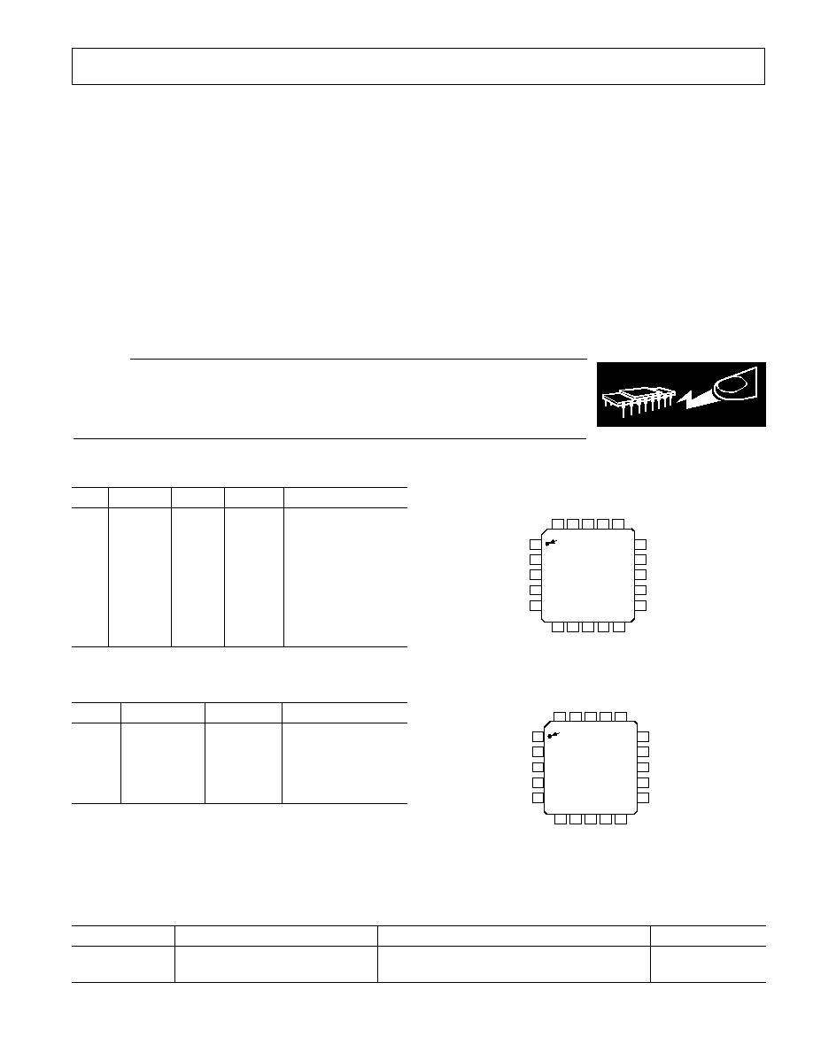
PIN CONFIGURATIONS
TOP VIEW
(Not to Scale)
PIN 1
IDENTIFIER
EN
V
SS
S1
S2
S3
GND
V
DD
S5
S6
S7
ADG758
NC
A0
A1
A2
NC
S4
D
NC
NC
S8
1
2
3
4
5
6
7
8
9
10
11
12
13
14
15
16
17
18
19
20
NC = NO CONNECT
EXPOSED PAD TIED TO SUBSTRATE, V
SS
TOP VIEW
(Not to Scale)
PIN 1
IDENTIFIER
EN
S1A
S2A
S3A
GND
V
DD
S1B
S2B
S3B
ADG759
NC
A0
NC
A1
NC
S4A
DA
NC
DB
S4B
1
2
3
4
5
6
7
8
9
10
11
12
13
14
15
16
17
18
19
20
NC = NO CONNECT
EXPOSED PAD TIED TO SUBSTRATE, V
SS
V
SS

ADG758/ADG759
6
REV. A
V
DD
Most Positive Power Supply Potential
V
SS
Most Negative Power Supply in a dual-supply application. In single-supply applications, this should be tied to
ground at the device.
GND
Ground (0 V) Reference
S
Source Terminal. May be an input or output.
D
Drain Terminal. May be an input or output.
IN
Logic Control Input
R
ON
Ohmic Resistance between D and S
R
FLAT(ON)
Flatness is defined as the difference between the maximum and minimum value of ON resistance as measured over
the specified analog signal range.
I
S
(OFF)
Source Leakage Current with the Switch OFF
I
D
(OFF)
Drain leakage Current with the Switch OFF
I
D
, I
S
(ON)
Channel Leakage current with the Switch ON
V
D
(V
S
)
Analog Voltage on Terminals D, S
C
S
(OFF)
OFF Switch Source Capacitance. Measured with reference to ground.
C
D
(OFF)
OFF Switch Drain Capacitance. Measured with reference to ground.
C
D
, C
S
(ON)
ON Switch Capacitance. Measured with reference to ground.
C
IN
Digital Input Capacitance
t
TRANSITION
Delay Time measured between the 50% and 90% points of the digital inputs and the switch ON condition when
switching from one address state to another.
t
ON
(EN)
Delay Time between the 50% and 90% points of the EN digital input and the switch ON condition.
t
OFF
(EN)
Delay Time between the 50% and 90% points of the EN digital input and the switch OFF condition.
t
OPEN
OFF Time measured between the 80% points of both switches when switching from one address state to another.
Off Isolation
A measure of unwanted signal coupling through an OFF switch.
Crosstalk
A measure of unwanted signal which is coupled through from one channel to another as a result of parasitic capacitance.
Charge
A measure of the glitch impulse transferred from the digital input to the analog output during switching.
Injection
On Response
The Frequency Response of the ON Switch.
On Loss
The Loss Due to the ON Resistance of the Switch
V
INL
Maximum Input Voltage for Logic "0"
V
INH
Minimum Input Voltage for Logic "1"
I
INL
(I
INH
)
Input Current of the Digital Input
I
DD
Positive Supply Current
I
SS
Negative Supply Current
TERMINOLOGY
ADG758/ADG759
7
REV. A
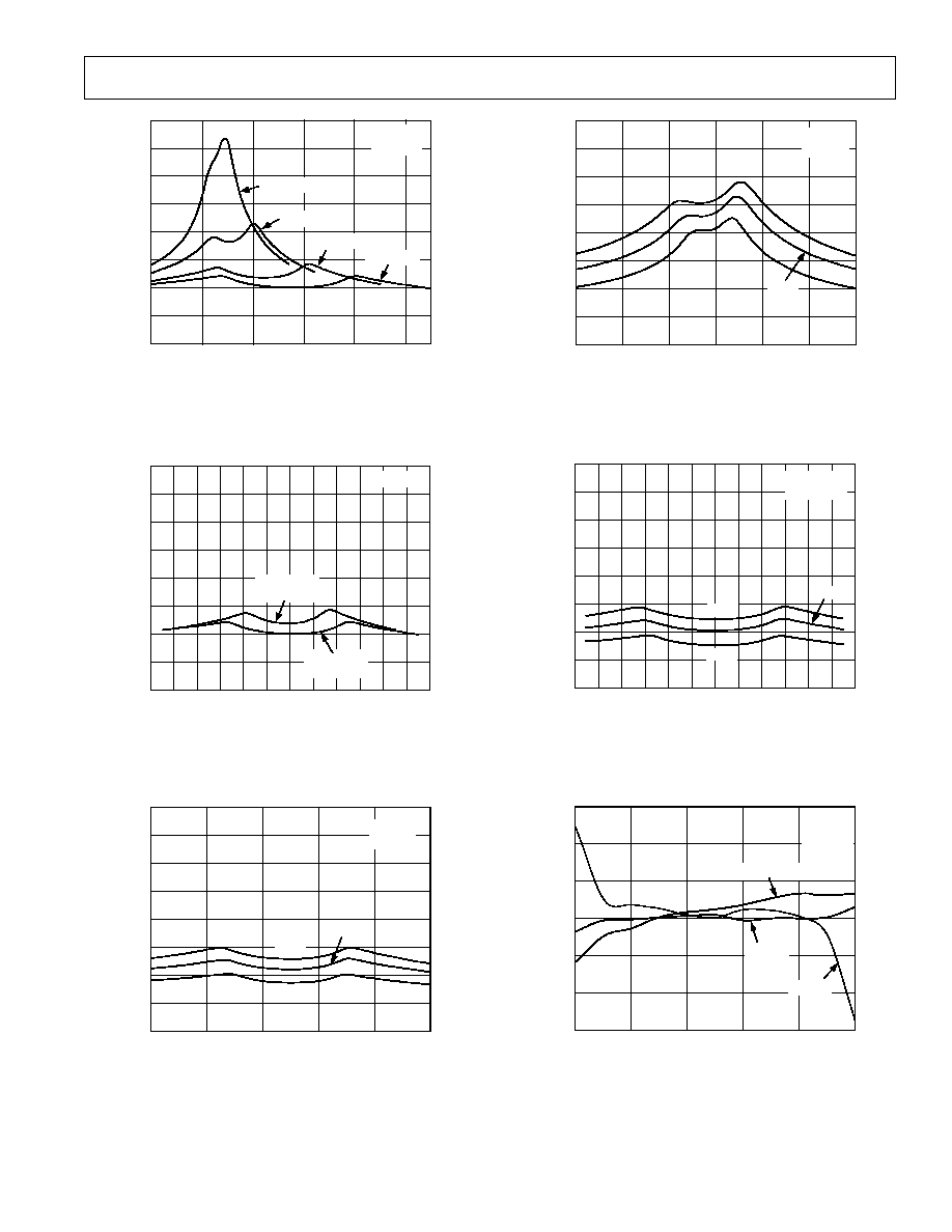
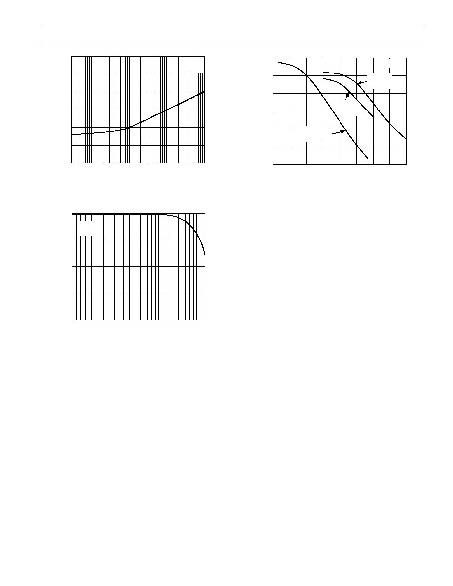
Typical Performance Characteristics
V
D
, V
S
, DRAIN OR SOURCE VOLTAGE V
8
0
1
2
3
4
5
T
A
= 25 C
V
SS
= 0V
7
6
5
4
3
2
1
0
ON RESISTANCE
V
DD
= 2.7V
V
DD
= 3.3V
V
DD
= 4.5V
V
DD
= 5.5V
TPC 1. ON Resistance as a Function of V
D
(V
S
) for Single
Supply
V
D
OR V
S
DRAIN OR SOURCE VOLTAGE V
8
3.0
T
A
= 25 C
7
6
5
4
3
2
0
ON RESISTANCE
2.5 2.0 1.5 1.0 0.5
1.0
1.5
2.0
2.5
3.0
0.5
0
V
DD
= +2.25V
V
SS
= 2.25V
V
DD
= +2.75V
V
SS
= 2.75V
1
TPC 2. ON Resistance as a Function of V
D
(V
S
) for Dual
Supply
V
D
OR V
S
DRAIN OR SOURCE VOLTAGE V
0
1
2
3
4
5
7
6
5
4
3
2
1
0
ON RESISTANCE
+85 C
+25 C
40 C
8
V
DD
= 5V
V
SS
= 0V
TPC 3. ON Resistance as a Function of V
D
(V
S
) for Different
Temperatures, Single Supply
V
D
OR V
S
DRAIN OR SOURCE VOLTAGE V
0
0.5
7
6
5
4
3
2
1
0
ON RESISTANCE
1.0
1.5
2.0
2.5
3.0
40 C
+25 C
+85 C
8
V
DD
= 3V
V
SS
= 0V
TPC 4. ON Resistance as a Function of V
D
(V
S
) for
Different Temperatures, Single Supply
V
D
OR V
S
DRAIN OR SOURCE VOLTAGE V
7
6
5
4
3
2
1
0
ON RESISTANCE
3.0 2.5 2.0 1.5 1.0
1.0
1.5
2.0
2.5
0.5
0
V
DD
= +2.5V
V
SS
= 2.5V
+85 C
+25 C
40 C
3.0
8
0.5
TPC 5. ON Resistance as a Function of V
D
(V
S
) for
Different Temperatures, Dual Supply
V
S
,
(V
D
= V
DD
V
S
) V
0
1
0.12
CURRENT nA
2
3
4
5
V
DD
= 5V
V
SS
= 0V
T
A
= 25 C
0.08
0.04
0.00
0.04
0.08
0.12
I
D
(ON), V
S
= V
D
I
S
(OFF)
I
D
(OFF)
TPC 6. Leakage Currents as a Function of V
D
(V
S
)
ADG758/ADG759
8
REV. A
0
0.5
0.12
CURRENT nA
1.0
1.5
2.0
3.0
V
DD
= 3V
V
SS
= 0V
T
A
= 25 C
0.08
0.04
0.00
0.04
0.08
0.12
2.5
I
S
(OFF)
I
D
(OFF)
V
S
, (V
D
= V
DD
V
S
) V
I
D
(ON), V
S
= V
D
TPC 7. Leakage Currents as a Function of V
D
(V
S
)
3.0
0.12
CURRENT nA
V
DD
= +2.5V
V
SS
= 2.5V
T
A
= 25 C
0.08
0.04
0.00
0.04
0.08
0.12
2.5 2.0 1.5 1.0
0
0.5
1.0
1.5
2.0
2.5
I
S
(OFF)
I
D
(OFF)
0.5
3.0
V
S
,
(V
D
= V
DD
V
S
) V
I
D
(ON), V
S
= V
D
TPC 8. Leakage Currents as a Function of V
D
(V
S
)
TEMPERATURE
C
15
CURRENT nA
V
DD
= 5V, V
SS
= 0V
V
DD
= +2.5V, V
SS
= 2.5V
0.05
0.00
0.05
0.10
0.15
0.20
0.25
0.30
0.35
25
35
45
55
65
75
85
I
D
(ON)
I
S
(OFF)
I
D
(OFF)
TPC 9. Leakage Currents as a Function of Temperature
TEMPERATURE
C
15
CURRENT nA
V
DD
= 3V
V
SS
= 0V
0.05
0.00
0.05
0.10
0.15
0.20
0.25
0.30
0.35
25
35
45
55
65
75
85
I
D
(ON)
I
S
(OFF)
I
D
(OFF)
TPC 10. Leakage Currents as a Function of Temperature
FREQUENCY Hz
10m
10
CURRENT A
1m
100
10
1
100n
10n
1n
100
1k
10k
100k
1M
10M
T
A
= 25 C
V
DD
= +2.5V
V
SS
= 2.5V
V
DD
= +3V
V
DD
= +5V
TPC 11. Supply Current vs. Input Switching Frequency
FREQUENCY Hz
0
30k
ATTENUATION dB
20
40
60
80
100
120
100k
1M
10M
100M
V
DD
= 5V
T
A
= 25 C
TPC 12. OFF Isolation vs. Frequency
ADG758/ADG759
9
REV. A
FREQUENCY Hz
0
30k
ATTENUATION dB
20
40
60
80
100
120
100k
1M
10M
100M
V
DD
= 5V
T
A
= 25 C
TPC 13. Crosstalk vs. Frequency
FREQUENCY Hz
0
30k
ATTENUATION dB
5
100k
1M
10M
100M
10
15
20
V
DD
= 5V
T
A
= 25 C
TPC 14. ON Response vs. Frequency
VOLTAGE V
3
2
20
Q
INJ
pC
1
1
2
5
T
A
= 25 C
10
0
10
20
40
3
30
0
4
V
DD
= 3V
V
SS
= 0V
V
DD
= +2.5V
V
SS
= 2.5V
V
DD
= 5V
V
SS
= 0V
TPC 15. Charge Injection vs. Source Voltage
ADG758/ADG759
10
REV. A
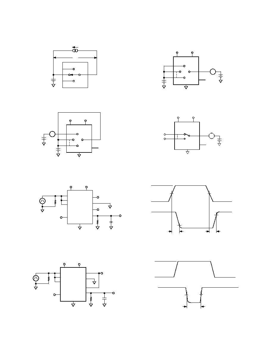
Test Circuits
R
ON
= V
1
/I
DS
V
S
V1
I
DS
D
S
Test Circuit 1. ON Resistance
V
D
A
0.8V
D
I
S
(OFF)
V
SS
V
DD
V
SS
V
DD
S1
S2
S8
EN
GND
V
S
Test Circuit 2. I
S
(OFF)
V
S
A
0.8V
D
I
D
(OFF)
V
SS
V
DD
V
SS
V
DD
S1
S2
S8
EN
GND
V
D
Test Circuit 3. I
D
(OFF)
A
2.4V
D
I
D
(ON)
V
SS
V
DD
V
SS
V
DD
S1
S8
EN
GND
V
D
NC
NC
NC = NO CONNECT
Test Circuit 4. I
D
(ON)
V
S8
3V
50%
t
TRANSITION
90%
90%
ADDRESS
DRIVE (V
IN
)
50%
0V
V
S1
V
OUT
t
TRANSITION
A2
D
*SIMILAR CONNECTION FOR ADG759
A1
A0
EN
GND
ADG758
*
S1
S8
S2 THRU S7
V
IN
2.4V
50
35pF
V
DD
V
SS
V
DD
V
SS
V
S1
V
S8
300
R
L
C
L
V
OUT
Test Circuit 5. Switching Time of Multiplexer, t
TRANSITION
t
OPEN
3V
80%
80%
ADDRESS
DRIVE (V
IN
)
0V
V
OUT
A2
D
*SIMILAR CONNECTION FOR ADG759
A1
A0
EN
GND
ADG758
*
S1
S8
S2 THRU S7
V
IN
2.4V
50
35pF
V
DD
V
SS
V
DD
V
SS
V
S
300
R
L
C
L
V
OUT
Test Circuit 6. Break-Before-Make Delay, t
OPEN
ADG758/ADG759
11
REV. A
OUTPUT
3V
50%
ENABLE
DRIVE (V
IN
)
50%
0V
V
0
t
ON
(EN)
0V
0.9V
0
0.9V
0
t
OFF
(EN)
A2
D
*SIMILAR CONNECTION FOR ADG759
A1
A0
EN
GND
ADG758*
S1
S2 THRU S8
V
IN
35pF
V
DD
V
SS
V
DD
V
SS
V
S
300
R
L
C
L
V
OUT
50
Test Circuit 7. Enable Delay, t
ON
(EN), t
OFF
(EN)
LOGIC INPUT
(V
IN
)
3V
0V
V
OUT
Q
INJ
= C
L
V
OUT
V
OUT
A2
V
OUT
V
DD
D
A1
A0
EN
GND
ADG758
*
C
L
1nF
V
DD
S
V
IN
R
S
V
SS
V
SS
V
S
*SIMILAR CONNECTION FOR ADG759
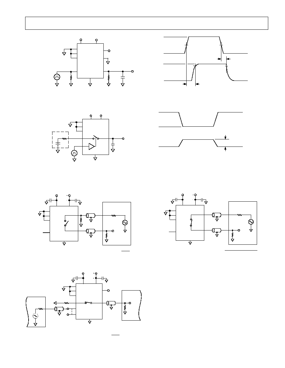
Test Circuit 8. Charge Injection
V
S
V
OUT
50
NETWORK
ANALYZER
R
L
50
GND
S
D
V
S
OFF ISOLATION = 20 LOG
V
OUT
0.1 F
V
DD
A2
A1
A0
EN
2.4V
0.1 F
V
SS
V
DD
V
SS
50
Test Circuit 9. OFF Isolation
*SIMILAR CONNECTION FOR ADG759
CHANNEL-TO-CHANNEL
CROSSTALK = 20
LOG
V
OUT
V
S
A2
D
A1
A0
EN
GND
ADG758
*
S1
S2
S8
2.4V
NETWORK
ANALYZER
NETWORK
ANALYZER
R
L
50
V
OUT
V
DD
0.1 F
V
SS
0.1 F
V
DD
V
SS
50
V
S
50
Test Circuit 10. Channel-to-Channel Crosstalk
V
S
V
OUT
50
NETWORK
ANALYZER
R
L
50
GND
S
D
V
OUT
WITH SWITCH
V
OUT
WITHOUT SWITCH
INSERTION LOSS = 20 LOG
0.1 F
V
DD
A2
A1
A0
EN
2.4V
0.1 F
V
SS
V
DD
V
SS
Test Circuit 11. Bandwidth
Power-Supply Sequencing
When using CMOS devices, care must be taken to ensure correct
power-supply sequencing. Incorrect power-supply sequencing
can result in the device being subjected to stresses beyond the
maximum ratings listed in the data sheet. Digital and analog
inputs should always be applied after power supplies and ground.
For single-supply operation, V
SS
should be tied to GND as close
to the device as possible.
12
C023710
5
/02(A)
PRINTED IN U.S.A.
ADG758/ADG759
REV. A
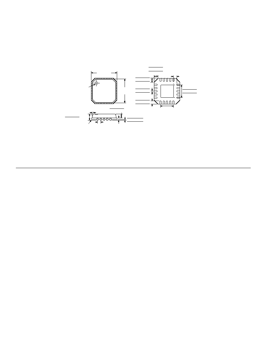
OUTLINE DIMENSIONS
Dimensions shown in inches and (mm).
20-Lead Chip Scale Package
(CP-20)
1
20
5
6
11
16
15
BOTTOM
VIEW
10
0.089 (2.25)
0.083 (2.10) SQ
0.077 (1.95)
0.024 (0.60)
0.017 (0.42)
0.009 (0.24)
0.024 (0.60)
0.017 (0.42)
0.009 (0.24)
0.030 (0.75)
0.024 (0.60)
0.020 (0.50)
0.012 (0.30)
0.009 (0.23)
0.007 (0.18)
0.080 (2.00)
REF
0.010 (0.25)
MIN
0.020 (0.50)
BSC
12
MAX
0.008 (0.20)
REF
0.028 (0.70) MAX
0.026 (0.65) NOM
0.002 (0.05)
0.0004 (0.01)
0.0 (0.0)
0.035 (0.90) MAX
0.033 (0.85) NOM
SEATING
PLANE
PIN 1
INDICATOR
TOP
VIEW
0.148 (3.75)
BSC SQ
0.157 (4.0)
BSC SQ
Revision History
Location
Page
Data Sheet changed from REV. 0 to REV. A.
Edits to General Description section . . . . . . . . . . . . . . . . . . . . . . . . . . . . . . . . . . . . . . . . . . . . . . . . . . . . . . . . . . . . . . . . . . . . . . . . . 1
Update Outline Drawings . . . . . . . . . . . . . . . . . . . . . . . . . . . . . . . . . . . . . . . . . . . . . . . . . . . . . . . . . . . . . . . . . . . . . . . . . . . . . . . . 12
Document Outline
- Specifications
- Pinout
- Package Drawings
- Ordering Guide
- Features
- Applications
- Product Description
- Absolute Maximum Ratings
- Functional Block Diagram
- Typical Characteristics
- CAUTION
- TERMINOLOGY
- DIAGRAMS
- Test Circuit 1. ON Resistance
- Test Circuit 2. IS (OFF)
- Test Circuit 3. ID (OFF)
- Test Circuit 4. ID (ON)
- Test Circuit 5. Switching Time of Multiplexer, tTRANSITION
- Test Circuit 6. Break-Before-Make Delay, tOPEN
- Test Circuit 7. Enable Delay, tON (EN), tOFF (EN)
- Test Circuit 8. Charge Injection
- Test Circuit 9. OFF Isolation
- Test Circuit 10. Channel-to-Channel Crosstalk
- Test Circuit 11. Bandwidth