 | ÐлекÑÑоннÑй компоненÑ: ADG774 | СкаÑаÑÑ:  PDF PDF  ZIP ZIP |
Äîêóìåíòàöèÿ è îïèñàíèÿ www.docs.chipfind.ru
REV. 0
Information furnished by Analog Devices is believed to be accurate and
reliable. However, no responsibility is assumed by Analog Devices for its
use, nor for any infringements of patents or other rights of third parties
which may result from its use. No license is granted by implication or
otherwise under any patent or patent rights of Analog Devices.
a
ADG774
One Technology Way, P.O. Box 9106, Norwood, MA 02062-9106, U.S.A.
Tel: 781/329-4700
World Wide Web Site: http://www.analog.com
Fax: 781/326-8703
© Analog Devices, Inc., 1998
CMOS
3 V/5 V, Wide Bandwidth Quad 2:1 Mux
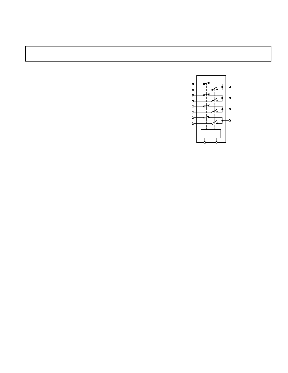
FUNCTIONAL BLOCK DIAGRAM
1 OF 2
DECODER
ADG774
EN
IN
S1A
S1B
S2A
S2B
S3A
S3B
S4A
S4B
D1
D2
D3
D4
FEATURES
Low Insertion Loss and On Resistance: 4 Typical
On-Resistance Flatness <2
Bandwidth >200 MHz
Single 3 V/5 V Supply Operation
Rail-to-Rail Operation
Very Low Distortion: <1%
Low Quiescent Supply Current (100 nA Typical)
Fast Switching Times
t
ON
10 ns
t
OFF
4 ns
TTL/CMOS Compatible
APPLICATIONS
10/100 Base-TX/T4
100VG-AnyLAN
Token Ring 4 Mbps/16 Mbps
ATM25/155
NIC Adapter and Hubs
Audio and Video Switching
Relay Replacement
GENERAL DESCRIPTION
The ADG774 is a monolithic CMOS device comprising four
2:1 multiplexer/demultiplexers with high impedance outputs.
The CMOS process provides low power dissipation yet gives
high switching speed and low on resistance. The on-resistance
variation is typically less than 0.5
with an input signal ranging
from 0 V to 5 V.
The bandwidth of the ADG774 is greater than 200 MHz and
this, coupled with low distortion (typically 0.5%), makes the
part suitable for switching fast ethernet signals.
The on-resistance profile is very flat over the full analog input
range ensuring excellent linearity and low distortion when switch-
ing audio signals. Fast switching speed, coupled with high signal
bandwidth, also makes the parts suitable for video signal switch-
ing. CMOS construction ensures ultralow power dissipation
making the parts ideally suited for portable and battery powered
instruments.
The ADG774 operates from a single 3.3 V/5 V supply and is
TTL logic compatible. The control logic for each switch is shown
in the Truth Table.
These switches conduct equally well in both directions when ON,
and have an input signal range that extends to the supplies. In
the OFF condition, signal levels up to the supplies are blocked.
The ADG774 switches exhibit break-before-make switching
action.
PRODUCT HIGHLIGHTS
1. Wide bandwidth data rates >200 MHz.
2. Ultralow Power Dissipation.
3. Extended Signal Range.
The ADG774 is fabricated on a CMOS process giving an
increased signal range that fully extends to the supply rails.
4. Low leakage over temperature.
5. Break-Before-Make Switching.
This prevents channel shorting when the switches are config-
ured as a multiplexer.
6. Crosstalk is typically 70 dB @ 30 MHz.
7. Off isolation is typically 60 dB @ 10 MHz.

2
REV. 0
ADG774SPECIFICATIONS
B Version
T
MIN
to
Parameter
+25 C
T
MAX
Units
Test Conditions/Comments
ANALOG SWITCH
Analog Signal Range
0 V to V
DD
V
On Resistance (R
ON
)
2.2
typ
V
D
= 0 V to V
DD
, I
S
= 10 mA
5
max
On Resistance Match Between
Channels (
R
ON
)
0.15
typ
V
D
= 0 V to V
DD
, I
S
= 10 mA
0.5
max
On Resistance Flatness (R
FLAT(ON)
)
0.5
typ
V
D
= 0 V to V
DD
; I
S
= 1 mA
1
max
LEAKAGE CURRENTS
Source OFF Leakage I
S
(OFF)
±
0.01
nA typ
V
D
= 4.5 V, V
S
= 1 V; V
D
= 1 V, V
S
= 4.5 V;
±
0.5
±
1
nA max
Test Circuit 2
Drain OFF Leakage I
D
(OFF)
±
0.01
nA typ
V
D
= 4.5 V, V
S
= 1 V; V
D
= 1 V, V
S
= 4.5 V;
±
0.5
±
1
nA max
Test Circuit 2
Channel ON Leakage I
D
, I
S
(ON)
±
0.01
nA typ
V
D
= V
S
= 4.5 V; V
D
= V
S
= 1 V; Test Circuit 3
±
0.5
±
1
nA max
DIGITAL INPUTS
Input High Voltage, V
INH
2.4
V min
Input Low Voltage, V
INL
0.8
V max
Input Current
I
INL
or I
INH
0.001
µ
A typ
V
IN
= V
INL
or V
INH
±
0.5
µ
A max
DYNAMIC CHARACTERISTICS
2
t
ON
10
ns typ
R
L
= 100
, C
L
= 35 pF,
20
ns max
V
S
= +3 V; Test Circuit 4
t
OFF
4
ns typ
R
L
= 100
, C
L
= 35 pF,
8
ns max
V
S
= +3 V; Test Circuit 4
Break-Before-Make Time Delay, t
D
5
ns typ
R
L
= 100
, C
L
= 35 pF,
1
ns min
V
S1
= V
S2
= +5 V; Test Circuit 5
Off Isolation
65
dB typ
R
L
= 100
, f = 10 MHz; Test Circuit 7
Channel-to-Channel Crosstalk
75
dB typ
R
L
= 100
, f = 10 MHz; Test Circuit 8
Bandwidth 3 dB
240
MHz typ
R
L
= 100
; Test Circuit 6
Distortion
0.5
% typ
R
L
= 100
Charge Injection
10
pC typ
C
L
= 1 nF; Test Circuit 9
C
S
(OFF)
10
pF typ
f = 1 kHz
C
D
(OFF)
20
pF typ
f = 1 kHz
C
D
, C
S
(ON)
30
pF typ
f = 1 MHz
POWER REQUIREMENTS
V
DD
= +5.5 V
Digital Inputs = 0 V or V
DD
I
DD
1
µ
A max
0.001
µ
A typ
I
IN
1
µ
A typ
V
IN
= +5 V
I
O
100
mA max
V
S
/V
D
= 0 V
NOTES
1
Temperature ranges are as follows: B Version, 40
°
C to +85
°
C.
2
Guaranteed by design, not subject to production test.
Specifications subject to change without notice.
(V
DD
= +5 V 10%, GND = 0 V. All specifications T
MIN
to T
MAX
unless otherwise noted.)
SINGLE SUPPLY

3
REV. 0
ADG774
B Version
T
MIN
to
Parameter
+25 C
T
MAX
Units
Test Conditions/Comments
ANALOG SWITCH
Analog Signal Range
0 V to V
DD
V
On Resistance (R
ON
)
4
typ
V
D
= 0 V to V
DD
, I
S
= 10 mA
8
max
On Resistance Match Between
Channels (
R
ON
)
0.15
typ
V
D
= 0 V to V
DD
, I
S
= 10 mA
0.5
max
On Resistance Flatness (R
FLAT(ON)
)
2
typ
V
D
= 0 V to V
DD
, I
S
= 10 mA
4
max
LEAKAGE CURRENTS
Source OFF Leakage I
S
(OFF)
±
0.01
nA typ
V
D
= 3 V, V
S
= 1 V; V
D
= 1 V, V
S
= 3 V;
±
0.5
±
1
nA max
Test Circuit 2
Drain OFF Leakage I
D
(OFF)
±
0.01
nA typ
V
D
= 3 V, V
S
= 1 V; V
D
= 1 V, V
S
= 3 V;
±
0.5
±
1
nA max
Test Circuit 2
Channel ON Leakage I
D
, I
S
(ON)
±
0.01
nA typ
V
D
= V
S
= 3 V; V
D
= V
S
= 1 V; Test Circuit 3
±
0.5
±
1
nA max
DIGITAL INPUTS
Input High Voltage, V
INH
2.0
V min
Input Low Voltage, V
INL
0.4
V max
Input Current
I
INL
or I
INH
0.001
µ
A typ
V
IN
= V
INL
or V
INH
±
0.5
µ
A max
DYNAMIC CHARACTERISTICS
2
t
ON
12
ns typ
R
L
= 100
, C
L
= 35 pF,
25
ns max
V
S
= +1.5 V; Test Circuit 4
t
OFF
5
ns typ
R
L
= 100
, C
L
= 35 pF,
10
ns max
V
S
= +1.5 V; Test Circuit 4
Break-Before-Make Time Delay, t
D
5
ns typ
R
L
= 100
, C
L
= 35 pF,
1
ns min
V
S1
= V
S2
= 3 V; Test Circuit 5
Off Isolation
65
dB typ
R
L
= 50
, f = 10 MHz; Test Circuit 7
Channel-to-Channel Crosstalk
75
dB typ
R
L
= 50
, f = 10 MHz; Test Circuit 8
Bandwidth 3 dB
240
MHz typ
R
L
= 50
; Test Circuit 6
Distortion
2
% typ
R
L
= 50
Charge Injection
3
pC typ
C
L
= 1 nF; Test Circuit 9
C
S
(OFF)
10
pF typ
f = 1 kHz
C
D
(OFF)
20
pF typ
f = 1 kHz
C
D
, C
S
(ON)
30
pF typ
f = 1 MHz
POWER REQUIREMENTS
V
DD
= +3.3 V
Digital Inputs = 0 V or V
DD
I
DD
1
µ
A max
0.001
µ
A typ
I
IN
1
µ
A typ
V
IN
= +3 V
I
O
100
mA max
V
S
/V
D
= 0 V
NOTES
1
Temperature ranges are as follows: B Version, 40
°
C to +85
°
C.
2
Guaranteed by design, not subject to production test.
Specifications subject to change without notice.
(V
DD
= +3 V 10%, GND = 0 V. All specifications T
MIN
to T
MAX
unless otherwise noted.)
SINGLE SUPPLY
Table I. Truth Table
EN
IN
D1
D2
D3
D4
Function
1
X
Hi-Z
Hi-Z
Hi-Z
Hi-Z
DISABLE
0
0
S1A
S2A
S3A
S4A
IN = 0
0
1
S1B
S2B
S3B
S4B
IN = 1
ADG774
4
REV. 0
ORDERING GUIDE
Model
Temperature Range
Package Descriptions
Package Options
ADG774BR
40
°
C to +85
°
C
R = 0.15" Small Outline IC (SOIC)
R-16A
ADG774BRQ
40
°
C to +85
°
C
RQ = 0.15" Quarter Size Outline Package (QSOP)
RQ-16
PIN CONFIGURATION
(SOIC/QSOP)
TOP VIEW
(Not to Scale)
16
15
14
13
12
11
10
9
1
2
3
4
5
6
7
8
IN
S1A
S1B
D1
S2A
S2B
D2
GND
V
DD
EN
S4A
S4B
D4
S3A
S3B
D3
ADG774
CAUTION
ESD (electrostatic discharge) sensitive device. Electrostatic charges as high as 4000 V readily
accumulate on the human body and test equipment and can discharge without detection.
Although the ADG774 features proprietary ESD protection circuitry, permanent damage may
occur on devices subjected to high energy electrostatic discharges. Therefore, proper ESD
precautions are recommended to avoid performance degradation or loss of functionality.
WARNING!
ESD SENSITIVE DEVICE
ABSOLUTE MAXIMUM RATINGS
1
(T
A
= +25
°
C unless otherwise noted)
V
DD
to GND . . . . . . . . . . . . . . . . . . . . . . . . . . . 0.3 V to +6 V
Analog, Digital Inputs
2
. . . . . . . . . . . 0.3 V to V
DD
+ 0.3 V or
30 mA, Whichever Occurs First
Continuous Current, S or D . . . . . . . . . . . . . . . . . . . . 100 mA
Peak Current, S or D . . . . . . . . . . . . . . . . . . . . . . . . . 300 mA
(Pulsed at 1 ms, 10% Duty Cycle max)
Operating Temperature Range
Industrial (B Version) . . . . . . . . . . . . . . . . . 40
°
C to +85
°
C
Storage Temperature Range . . . . . . . . . . . . . 65
°
C to +150
°
C
Junction Temperature . . . . . . . . . . . . . . . . . . . . . . . . . +150
°
C
SOIC Package, Power Dissipation . . . . . . . . . . . . . . . . 600 mW
JA
Thermal Impedance . . . . . . . . . . . . . . . . . . . . . 100
°
C/W
Lead Temperature, Soldering
Vapor Phase (60 sec) . . . . . . . . . . . . . . . . . . . . . . . . +215
°
C
Infrared (15 sec) . . . . . . . . . . . . . . . . . . . . . . . . . . . . +220
°
C
QSOP Package, Power Dissipation . . . . . . . . . . . . . . . 566 mW
JA
Thermal Impedance . . . . . . . . . . . . . . . . . . . 149.97
°
C/W
Lead Temperature, Soldering
Vapor Phase (60 sec) . . . . . . . . . . . . . . . . . . . . . . . . +215
°
C
Infrared (15 sec) . . . . . . . . . . . . . . . . . . . . . . . . . . . . +220
°
C
ESD . . . . . . . . . . . . . . . . . . . . . . . . . . . . . . . . . . . . . . . . . . 2 kV
NOTES
1
Stresses above those listed under Absolute Maximum Ratings may cause perma-
nent damage to the device. This is a stress rating only; functional operation of the
device at these or any other conditions above those listed in the operational sections
of this specification is not implied. Exposure to absolute maximum rating condi-
tions for extended periods may affect device reliability. Only one absolute maxi-
mum rating may be applied at any one time.
2
Overvoltages at IN, S or D will be clamped by internal diodes. Current should be
limited to the maximum ratings given.
TERMINOLOGY
V
DD
Most Positive Power Supply Potential.
GND
Ground (0 V) Reference.
S
Source Terminal. May be an input or output.
D
Drain Terminal. May be an input or output.
IN
Logic Control Input.
EN
Logic Control Input.
R
ON
Ohmic resistance between D and S.
R
ON
On Resistance match between any two channels
i.e., R
ON
max R
ON
min.
R
FLAT(ON)
Flatness is defined as the difference between the
maximum and minimum value of on resistance
as measured over the specified analog signal
range.
I
S
(OFF)
Source Leakage Current with the switch "OFF."
I
D
(OFF)
Drain Leakage Current with the switch "OFF."
I
D
, I
S
(ON)
Channel Leakage Current with the switch "ON."
V
D
(V
S
)
Analog Voltage on Terminals D, S.
C
S
(OFF)
"OFF" Switch Source Capacitance.
C
D
(OFF)
"OFF" Switch Drain Capacitance.
C
D
, C
S
(ON) "ON" Switch Capacitance.
t
ON
Delay between applying the digital control input
and the output switching on. See Test Circuit 4.
t
OFF
Delay between applying the digital control input
and the output switching Off.
t
D
"OFF" time or "ON" time measured between
the 90% points of both switches, when switching
from one address state to another. See Test
Circuit 5.
Crosstalk
A measure of unwanted signal that is coupled
through from one channel to another as a result
of parasitic capacitance.
Off Isolation A measure of unwanted signal coupling through an
"OFF" switch.
Bandwidth
Frequency response of the switch in the ON
state measured at 3 dB down.
Distortion
R
FLAT(ON)
/R
L
T
A
= +25 C
V
S
OR V
D
DRAIN OR SOURCE VOLTAGE V
1.3
2.5
3.7
4.9
5.0
4.5
0
R
ON
2.0
1.5
1.0
0.5
3.0
2.5
3.5
4.0
V
DD
= +2.7V
V
DD
= +3.0V
V
DD
= +4.5V
V
DD
= +5.0V
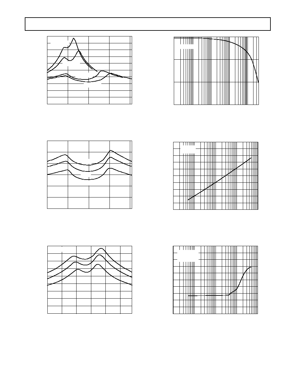
Figure 1. On Resistance as a Function of V
D
(V
S
) for
Various Single Supplies
V
DD
= +5V
3.0
0
R
ON
1.5
1.0
0.5
2.0
2.5
V
S
OR V
O
DRAIN OR SOURCE VOLTAGE V
1.3
2.5
3.7
4.9
+85 C
+25 C
40 C
Figure 2. On Resistance as a Function of V
D
(V
S
) for
Different Temperatures with 5 V Single Supplies
+85 C
+25 C
40 C
4.5
0
R
ON
2.0
1.5
1.0
3.0
2.5
3.5
4.0
0.5
V
DD
= +3V
V
S
OR V
D
DRAIN OR SOURCE VOLTAGE V
0.6
1.1
1.6
2.1
2.6
Figure 3. On Resistance as a Function of V
D
(V
S
) for
Different Temperatures with 3 V Single Supplies
Typical Performance CharacteristicsADG774
5
REV. 0
V
DD
= +5V
FREQUENCY Hz
0
10M
10k
ON RESPONSE dB
4
2
100k
1M
100M
6
Figure 4. On Response vs. Frequency
FREQUENCY Hz
0
10
100
100k
1G
1M
10M
100M
40
70
80
90
20
30
60
50
ATTENUATION dB
V
DD
= +5V
R
L
= 100
Figure 5. Off Isolation vs. Frequency
FREQUENCY Hz
0
10
100
100k
1G
1M
10M
100M
40
70
80
90
20
30
60
50
ATTENUATION dB
V
DD
= +5V
R
L
= 100
V
P-P
= 0.316V
Figure 6. Crosstalk vs. Frequency
ADG774
6
REV. 0
SOURCE VOLTAGE V
20
5
10
15
10
0
5
0
5.0
0.5
1.0
1.5
2.0
2.5
3.0
3.5
4.0
4.5
CHARGE INJECTION pC
V
DD
= +5V
T
A
= +25 C
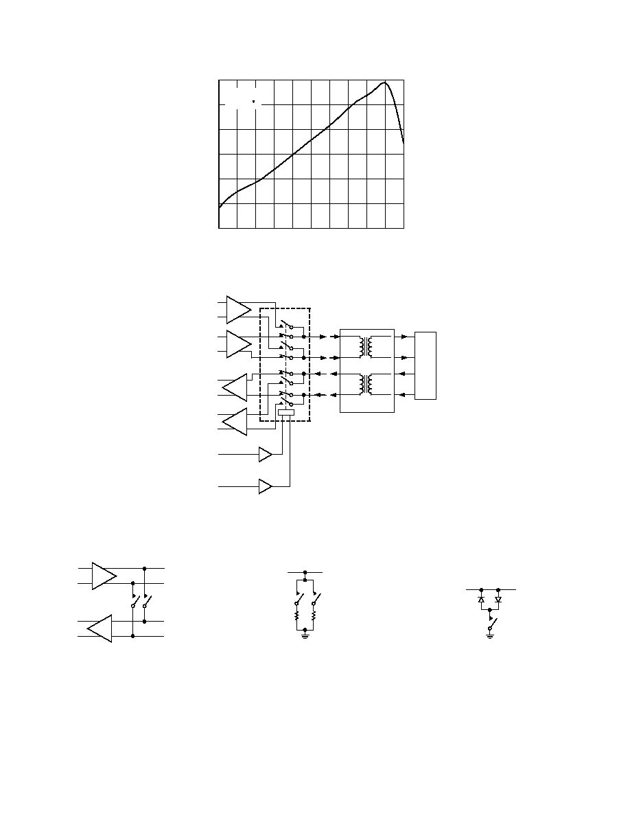
Figure 7. Charge Injection vs. Source Voltage
ADG774
TRANSFORMER
TX1
TX2
RX1
RX2
10 BASE TX+
10 BASE TX
100 BASE TX+
100 BASE TX
10 BASE TX+
10 BASE TX
100 BASE TX+
100 BASE TX
10 BASE TX
100 BASE TX
RJ45
Figure 8. Full Duplex Transceiver
Figure 11. Line Clamp
120
100
Figure 10. Line Termination
TX1
RX1
Figure 9. Loop Back
ADG774
7
REV. 0
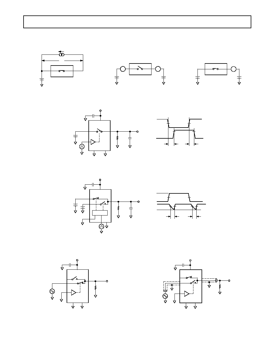
Test Circuits
I
DS
V1
S
D
V
S
R
ON
= V1/I
DS
Test Circuit 1. On Resistance
S
D
V
S
A
A
V
D
I
S
(OFF)
I
D
(OFF)
Test Circuit 2. Off Leakage
S
D
V
S
A
V
D
I
D
(ON)
Test Circuit 3. On Leakage
0.1 F
+5V
V
S
IN
S
D
V
DD
GND
R
L
100
C
L
35pF
V
OUT
EN
3V
50%
50%
90%
90%
V
IN
V
OUT
t
ON
t
OFF
Test Circuit 4. Switching Times
0.1 F
+5V
V
S
EN
S1A
D1
V
DD
GND
R
L
100
C
L
35pF
V
OUT
S1B
DECODER
V
S
50%
50%
V
IN
V
OUT
t
D
t
D
50%
50%
3V
0V
V
S
Test Circuit 5. Break-Before-Make Time Delay
0.1 F
+5V
V
S
IN
D1
V
DD
GND
R
L
100
V
OUT
V
IN
EN
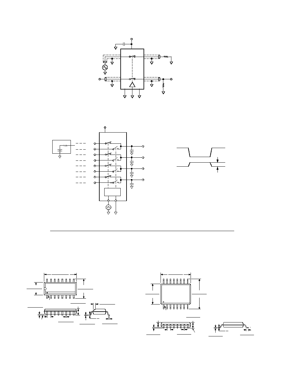
Test Circuit 6. Bandwidth
0.1 F
+5V
V
S
IN
D1
V
DD
GND
R
L
100
V
OUT
V
IN
EN
S1A
S1B
Test Circuit 7. Off Isolation
ADG774
8
REV. 0
PRINTED IN U.S.A.
C332687/98
OUTLINE DIMENSIONS
Dimensions shown in inches and (mm).
16-Lead SOIC
(R-16A)
16
9
8
1
0.3937 (10.00)
0.3859 (9.80)
0.2550 (6.20)
0.2284 (5.80)
0.1574 (4.00)
0.1497 (3.80)
PIN 1
SEATING
PLANE
0.0098 (0.25)
0.0040 (0.10)
0.0192 (0.49)
0.0138 (0.35)
0.0688 (1.75)
0.0532 (1.35)
0.0500
(1.27)
BSC
0.0099 (0.25)
0.0075 (0.19)
0.0500 (1.27)
0.0160 (0.41)
8
0
0.0196 (0.50)
0.0099 (0.25)
45
0.1 F
+5V
V
S
D1
V
DD
GND
EN
S1A
S2A
100
V
IN
D2
NC
V
OUT
R
L
100
CHANNEL-TO-CHANNEL
CROSSTALK = 20 LOG |V
S
/V
OUT
|
Test Circuit 8. Channel-to-Channel Crosstalk
+5V
EN
S1A
V
DD
C
L
1nF
S1B
V
IN
V
OUT
3V
V
OUT
Q
INJ
= C
L
V
OUT
C
L
1nF
C
L
1nF
C
L
1nF
D1 V
OUT
D2 V
OUT
D3 V
OUT
D4 V
OUT
ADG774
1 OF 2
DECODER
IN
S2A
S2B
S3A
S3B
S4A
S4B
V
S
R
S
Test Circuit 9. Charge Injection
16-Lead QSOP
(RQ-16)
16
9
8
1
0.197 (5.00)
0.189 (4.80)
0.244 (6.20)
0.228 (5.79)
PIN 1
0.157 (3.99)
0.150 (3.81)
SEATING
PLANE
0.010 (0.25)
0.004 (0.10)
0.012 (0.30)
0.008 (0.20)
0.025
(0.64)
BSC
0.059 (1.50)
MAX
0.069 (1.75)
0.053 (1.35)
0.010 (0.20)
0.007 (0.18)
0.050 (1.27)
0.016 (0.41)
8
0