 | ÐлекÑÑоннÑй компоненÑ: ADG782 | СкаÑаÑÑ:  PDF PDF  ZIP ZIP |
Äîêóìåíòàöèÿ è îïèñàíèÿ www.docs.chipfind.ru
REV. A
Information furnished by Analog Devices is believed to be accurate and
reliable. However, no responsibility is assumed by Analog Devices for its
use, nor for any infringements of patents or other rights of third parties that
may result from its use. No license is granted by implication or otherwise
under any patent or patent rights of Analog Devices.
a
ADG781/ADG782/ADG783
One Technology Way, P.O. Box 9106, Norwood, MA 02062-9106, U.S.A.
Tel: 781/329-4700
www.analog.com
Fax: 781/326-8703
© Analog Devices, Inc., 2002
2.5
Quad SPST Switches
in Chip Scale Package
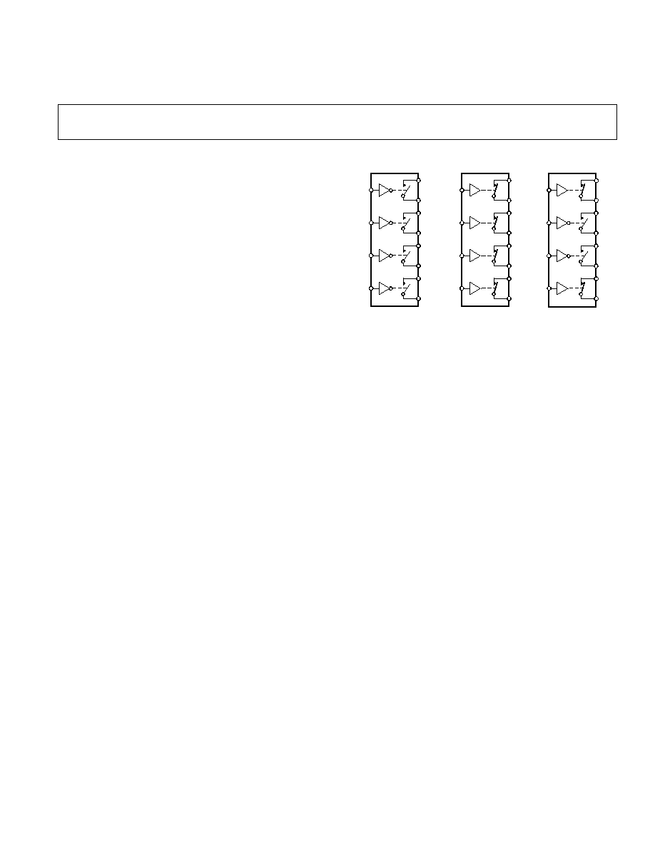
FUNCTIONAL BLOCK DIAGRAMS
IN1
IN2
IN3
IN4
S1
D1
S2
D2
S3
D3
S4
D4
ADG781
SWITCHES SHOWN FOR A LOGIC "1" INPUT
IN1
IN2
IN3
IN4
S1
D1
S2
D2
S3
D3
S4
D4
ADG782
IN1
IN2
IN3
IN4
S1
D1
S2
D2
S3
D3
S4
D4
ADG783
FEATURES
1.8 V to 5.5 V Single Supply
Low On Resistance (2.5 Typ)
Low On-Resistance Flatness (0.5 )
3 dB Bandwidth > 200 MHz
Rail-to-Rail Operation
20-Lead 4 mm 4 mm Chip Scale Package
Fast Switching Times
t
ON
= 16 ns
t
OFF
= 10 ns
Typical Power Consumption (< 0.01 W)
TTL/CMOS Compatible
For Functionally Equivalent Devices in 16-Lead TSSOP
and SOIC Packages, See ADG711/ADG712/ADG713
APPLICATIONS
Battery Powered Systems
Communication Systems
Sample Hold Systems
Audio Signal Routing
Video Switching
Mechanical Reed Relay Replacement
GENERAL DESCRIPTION
The ADG781, ADG782, and ADG783 are monolithic CMOS
devices containing four independently selectable switches. These
switches are designed on an advanced submicron process that
provides low power dissipation and high switching speed, low on
resistance, low leakage currents and high bandwidth.
They are designed to operate from a single 1.8 V to 5.5 V sup-
ply, making them ideal for use in battery powered instruments
and with the new generation of DACs and ADCs from Analog
Devices. Fast switching times and high bandwidth make the
part suitable for video signal switching.
The ADG781, ADG782, and ADG783 contain four independent
single-pole/single throw (SPST) switches. The ADG781 and
ADG782 differ only in that the digital control logic is inverted.
The ADG781 switches are turned on with a logic low on the
appropriate control input, while a logic high is required to turn
on the switches of the ADG782. The ADG783 contains two
switches whose digital control logic is similar to the ADG781,
while the logic is inverted on the other two switches.
Each switch conducts equally well in both directions when ON.
The ADG783 exhibits break-before-make switching action.
The ADG781/ADG782/ADG783 are available in 20-lead chip
scale packages.
PRODUCT HIGHLIGHTS
1. 20-Lead 4 mm 4 mm Chip Scale Package (CSP).
2. 1.8 V to 5.5 V Single Supply Operation. The ADG781,
ADG782, and ADG783 offer high performance and are
fully specified and guaranteed with 3 V and 5 V supply
rails.
3. Very Low R
ON
(4.5
max at 5 V, 8 max at 3 V). At supply
voltage of 1.8 V, R
ON
is typically 35
over the temperature
range.
4. Low On-Resistance Flatness.
5. 3 dB Bandwidth >200 MHz.
6. Low Power Dissipation. CMOS construction ensures low
power dissipation.
7. Fast t
ON
/t
OFF.
8. Break-Before-Make Switching. This prevents channel shorting
when the switches are configured as a multiplexer (ADG783
only).

REV. A
2
ADG781/ADG782/ADG783SPECIFICATIONS
(V
DD
= 5 V 10%, GND = 0 V. All specifications
40 C to +85 C
unless otherwise noted.)
B Version
40 C to
Parameter
+25 C
+85 C
Unit
Test Conditions/Comments
ANALOG SWITCH
Analog Signal Range
0 V to V
DD
V
On Resistance (R
ON
)
2.5
typ
V
S
= 0 V to V
DD
, I
S
= 10 mA;
4
4.5
max
Test Circuit 1
On-Resistance Match Between
0.05
typ
V
S
= 0 V to V
DD
, I
S
= 10 mA
Channels (
R
ON
)
0.4
max
On-Resistance Flatness (R
FLAT(ON)
)
0.5
typ
V
S
= 0 V to V
DD
, I
S
= 10 mA
1.0
max
LEAKAGE CURRENTS
V
DD
= 5.5 V;
Source OFF Leakage I
S
(OFF)
±0.01
nA typ
V
S
= 4.5 V/1 V, V
D
= 1 V/4.5 V;
±0.1
±0.2
nA max
Test Circuit 2
Drain OFF Leakage I
D
(OFF)
±0.01
nA typ
V
S
= 4.5 V/1 V, V
D
= 1 V/4.5 V;
±0.1
±0.2
nA max
Test Circuit 2
Channel ON Leakage I
D
, I
S
(ON)
±0.01
nA typ
V
S
= V
D
= 1 V, or 4.5 V;
±0.1
±0.2
nA max
Test Circuit 3
DIGITAL INPUTS
Input High Voltage, V
INH
2.4
V min
Input Low Voltage, V
INL
0.8
V max
Input Current
I
INL
or I
INH
0.005
µA typ
V
IN
= V
INL
or V
INH
±0.1
µA max
DYNAMIC CHARACTERISTICS
2
t
ON
11
ns typ
R
L
= 300
, C
L
= 35 pF,
16
ns max
V
S
= 3 V; Test Circuit 4
t
OFF
6
ns typ
R
L
= 300
, C
L
= 35 pF,
10
ns max
V
S
= 3 V; Test Circuit 4
Break-Before-Make Time Delay, t
D
6
ns typ
R
L
= 300
, C
L
= 35 pF,
(ADG783 Only)
1
ns min
V
S1
= V
S2
= 3 V; Test Circuit 5
Charge Injection
3
pC typ
V
S
= 2 V; R
S
= 0
, C
L
= 1 nF;
Test Circuit 6
Off Isolation
58
dB typ
R
L
= 50
, C
L
= 5 pF, f = 10 MHz
78
dB typ
R
L
= 50
, C
L
= 5 pF, f = 1 MHz;
Test Circuit 7
Channel-to-Channel Crosstalk
90
dB typ
R
L
= 50
, C
L
= 5 pF, f = 10 MHz;
Test Circuit 8
Bandwidth 3 dB
200
MHz typ
R
L
= 50
, C
L
= 5 pF; Test Circuit 9
C
S
(OFF)
10
pF typ
f = 1 MHz
C
D
(OFF)
10
pF typ
f = 1 MHz
C
D
, C
S
(ON)
22
pF typ
f = 1 MHz
POWER REQUIREMENTS
V
DD
= 5.5 V
I
DD
0.001
µA typ
Digital Inputs = 0 V or 5.5 V
1.0
µA max
NOTES
1
Temperature ranges are as follows: B Version: 40
°C to +85°C.
2
Guaranteed by design, not subject to production test.
Specifications subject to change without notice.

REV. A
3
ADG781/ADG782/ADG783
B Version
40 C to
Parameter
+25 C
+85 C
Unit
Test Conditions/Comments
ANALOG SWITCH
Analog Signal Range
0 V to V
DD
V
On Resistance (R
ON
)
5
5.5
typ
V
S
= 0 V to V
DD
, I
S
= 10 mA;
10
max
Test Circuit 1
On-Resistance Match Between
0.1
typ
V
S
= 0 V to V
DD
, I
S
= 10 mA
Channels (
R
ON
)
0.5
max
On-Resistance Flatness (R
FLAT(ON)
)
2.5
typ
V
S
= 0 V to V
DD
, I
S
= 10 mA
LEAKAGE CURRENTS
V
DD
= 3.3 V;
Source OFF Leakage I
S
(OFF)
±0.01
nA typ
V
S
= 3 V/1 V, V
D
= 1 V/3 V;
±0.1
±0.2
nA max
Test Circuit 2
Drain OFF Leakage I
D
(OFF)
±0.01
nA typ
V
S
= 3 V/1 V, V
D
= 1 V/3 V;
±0.1
±0.2
nA max
Test Circuit 2
Channel ON Leakage I
D
, I
S
(ON)
±0.01
nA typ
V
S
= V
D
= 1 V, or 3 V;
±0.1
±0.2
nA max
Test Circuit 3
DIGITAL INPUTS
Input High Voltage, V
INH
2.0
V min
Input Low Voltage, V
INL
0.8
V max
Input Current
I
INL
or I
INH
0.005
µA typ
V
IN
= V
INL
or V
INH
±0.1
µA max
DYNAMIC CHARACTERISTICS
2
t
ON
13
ns typ
R
L
= 300
, C
L
= 35 pF,
20
ns max
V
S
= 2 V; Test Circuit 4
t
OFF
7
ns typ
R
L
= 300
, C
L
= 35 pF,
12
ns max
V
S
= 2 V; Test Circuit 4
Break-Before-Make Time Delay, t
D
7
ns typ
R
L
= 300
, C
L
= 35 pF,
(ADG783 Only)
1
ns min
V
S1
= V
S2
= 2 V; Test Circuit 5
Charge Injection
3
pC typ
V
S
= 1.5 V; R
S
= 0
, C
L
= 1 nF;
Test Circuit 6
Off Isolation
58
dB typ
R
L
= 50
, C
L
= 5 pF, f = 10 MHz
78
dB typ
R
L
= 50
, C
L
= 5 pF, f = 1 MHz;
Test Circuit 7
Channel-to-Channel Crosstalk
90
dB typ
R
L
= 50
, C
L
= 5 pF, f = 10 MHz;
Test Circuit 8
Bandwidth 3 dB
200
MHz typ
R
L
= 50
, C
L
= 5 pF; Test Circuit 9
C
S
(OFF)
10
pF typ
f = 1 MHz
C
D
(OFF)
10
pF typ
f = 1 MHz
C
D
, C
S
(ON)
22
pF typ
f = 1 MHz
POWER REQUIREMENTS
V
DD
= 3.3 V
I
DD
0.001
µA typ
Digital Inputs = 0 V or 3.3 V
1.0
µA max
NOTES
1
Temperature ranges are as follows: B Version: 40
°C to +85°C.
2
Guaranteed by design, not subject to production test.
Specifications subject to change without notice.
SPECIFICATIONS
1
(V
DD
= 3 V 10%, GND = 0 V. All specifications 40 C to +85 C
unless otherwise noted.)
REV. A
ADG781/ADG782/ADG783
4
ABSOLUTE MAXIMUM RATINGS
1
(T
A
= 25
°C unless otherwise noted.)
V
DD
to GND . . . . . . . . . . . . . . . . . . . . . . . . . . 0.3 V to +6 V
Analog, Digital Inputs
2
. . . . . . . . . . 0.3 V to V
DD
+ 0.3 V or
30 mA, Whichever Occurs First
Continuous Current, S or D . . . . . . . . . . . . . . . . . . . . . 30 mA
Peak Current, S or D . . . . . . . . . . . . . . . . . . . . . . . . . 100 mA
(Pulsed at 1 ms, 10% Duty Cycle max)
Operating Temperature Range
Industrial (B Version) . . . . . . . . . . . . . . . . 40
°C to +85°C
Storage Temperature Range . . . . . . . . . . . . 65
°C to +150°C
Junction Temperature . . . . . . . . . . . . . . . . . . . . . . . . . 150
°C
Chip Scale Package
JA
Thermal Impedance . . . . . . . . . . . . . . . . . . . . . 32
°C/W
ORDERING GUIDE
Model
Temperature Range
Package Description
Package Option
ADG781BCP
40
°C to +85°C
20-Lead Chip Scale (CSP)
CP-20
ADG782BCP
40
°C to +85°C
20-Lead Chip Scale (CSP)
CP-20
ADG783BCP
40
°C to +85°C
20-Lead Chip Scale (CSP)
CP-20
Lead Temperature, Soldering (10 sec) . . . . . . . . . . . . 300
°C
IR Reflow (<20 sec) . . . . . . . . . . . . . . . . . . . . . . . . . 235
°C
NOTES
1
Stresses above those listed under Absolute Maximum Ratings may cause perma-
nent damage to the device. This is a stress rating only; functional operation of the
device at these or any other conditions above those listed in the operational
sections of this specification is not implied. Exposure to absolute maximum rating
conditions for extended periods may affect device reliability. Only one absolute
maximum rating may be applied at any one time.
2
Overvoltages at IN, S, or D will be clamped by internal diodes. Current should be
limited to the maximum ratings given.
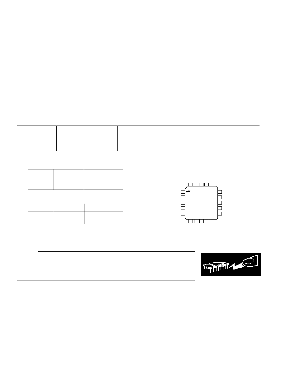
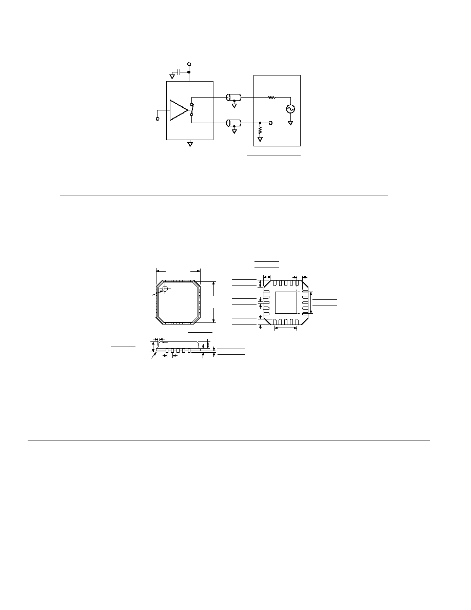
PIN CONFIGURATION
(CSP)
TOP VIEW
(Not to Scale)
PIN 1
IDENTIFIER
D1
S1
GND
S4
D4
D2
S2
V
DD
S3
D3
ADG781/ADG782/
ADG783
NC
IN1
NC
IN2
NC
NC
IN4
NC
IN3
NC
1
2
3
4
5
6
7
8
9
10
11
12
13
14
15
16
17
18
19
20
NC = NO CONNECT
EXPOSED PAD TIED TO SUBSTRATE, GND
Table I. Truth Table (ADG781/ADG782)
ADG781 In
ADG782 In
Switch Condition
0
1
ON
1
0
OFF
Table II. Truth Table (ADG783)
Logic
Switch 1, 4
Switch 2, 3
0
OFF
ON
1
ON
OFF
CAUTION
ESD (electrostatic discharge) sensitive device. Electrostatic charges as high as 4000 V readily
accumulate on the human body and test equipment and can discharge without detection.
Although the ADG781/ADG782/ADG783 feature proprietary ESD protection circuitry, permanent
damage may occur on devices subjected to high-energy electrostatic discharges. Therefore, proper
ESD precautions are recommended to avoid performance degradation or loss of functionality.
WARNING!
ESD SENSITIVE DEVICE
REV. A
ADG781/ADG782/ADG783
5
V
DD
Most positive power supply potential.
GND
Ground (0 V) reference.
S
Source terminal. May be an input or output.
D
Drain terminal. May be an input or output.
IN
Logic control input.
R
ON
Ohmic resistance between D and S.
R
ON
On-resistance match between any two chan-
nels (i.e., R
ON
max and R
ON
min).
R
FLAT(ON)
Flatness is defined as the difference between
the maximum and minimum value of on
resistance as measured over the specified
analog signal range.
I
S
(OFF)
Source leakage current with the switch "OFF."
I
D
(OFF)
Drain leakage current with the switch "OFF."
I
D
, I
S
(ON)
Channel leakage current with the switch "ON."
V
D
(V
S
)
Analog voltage on terminals D, S.
C
S
(OFF)
"OFF" switch source capacitance.
C
D
(OFF)
"OFF" switch drain capacitance.
C
D
, C
S
(ON)
"ON" switch capacitance.
t
ON
Delay between applying the digital control
input and the output switching on.
t
OFF
Delay between applying the digital control
input and the output switching off.
t
D
"OFF" time or "ON" time measured
between the 90% points of both switches,
when switching from one address state to
another (ADG783 only).
Crosstalk
A measure of unwanted signal that is coupled
through from one channel to another as a
result of parasitic capacitance.
Off Isolation
A measure of unwanted signal coupling
through an "OFF" switch.
Charge
A measure of the glitch impulse transferred
Injection
from the digital input to the analog output
during switching.
On Response
The frequency response of the "ON" switch.
On Loss
The loss due to the on resistance of the switch.
TERMINOLOGY
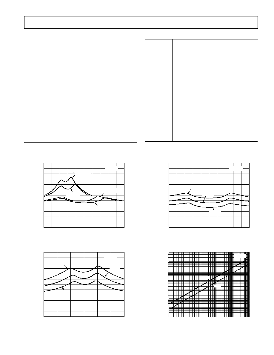
Typical Performance Characteristics
V
D
OR V
S
DRAIN OR SOURCE VOLTAGE V
6
R
ON
0
0
0.5
V
DD
= 2.7V
0.5
1
5.5
5
4.5
4
3.5
3
2.5
2
1.5
1
1.5
2
2.5
3
3.5
4
4.5
V
DD
= 3V
V
DD
= 4.5V
V
DD
= 5V
T
A
= 25 C
5
TPC 1. On Resistance as a Function of V
D
(V
S
)
V
D
OR V
S
DRAIN OR SOURCE VOLTAGE V
6
R
ON
0
0
+85 C
0.5
1
5.5
5
4.5
4
3.5
3
2.5
2
1.5
1
3
V
DD
= 3V
40 C
0.5
1.5
2
2.5
+25 C
TPC 2. On Resistance as a Function of V
D
(V
S
) for
Different Temperatures V
DD
= 3 V
V
D
OR V
S
DRAIN OR SOURCE VOLTAGE V
6
R
ON
0
0
0.5
0.5
1
5.5
5
4.5
4
3.5
3
2.5
2
1.5
1
1.5
2
2.5
3
3.5
4
4.5
5
V
DD
= 5V
+85 C
40 C
+25 C
TPC 3. On Resistance as a Function of V
D
(V
S
) for
Different Temperatures V
DD
= 5 V
V
DD
= 5V
4 SW
1 SW
FREQUENCY Hz
10m
1m
1n
100
10M
1k
I
SUPPLY
Amps
10k
100k
1M
100
10
1
100n
10n
TPC 4. Supply Current vs. Input Switching Frequency
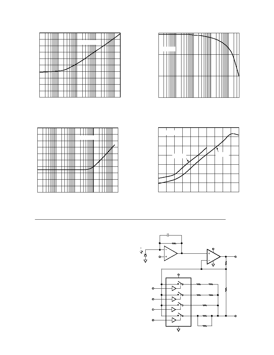
REV. A
ADG781/ADG782/ADG783
6
FREQUENCY Hz
30
OFF ISOLATION
dB
40
110
120
130
10k
100k
1M
10M
100M
100
90
80
70
60
50
V
DD
= 5V, 3V
TPC 5. Off Isolation vs. Frequency
FREQUENCY Hz
30
CROSSTALK
dB
40
110
120
130
10k
100k
1M
10M
V
DD
= 5V, 3V
100M
100
90
80
70
60
50
TPC 6. Crosstalk vs. Frequency
FREQUENCY Hz
0
ON RESPONSE
dB
6
10k
100k
1M
10M
V
DD
= 5V
100M
4
2
TPC 7. On Response vs. Frequency
SOURCE VOLTAGE V
25
Q
INJ
pC
10
0
0.5
5
0
20
15
10
5
1
1.5
2
2.5
3
3.5
4
4.5
5
V
DD
= 5V
V
DD
= 3V
T
A
= 25 C
TPC 8. Charge Injection vs. Source Voltage
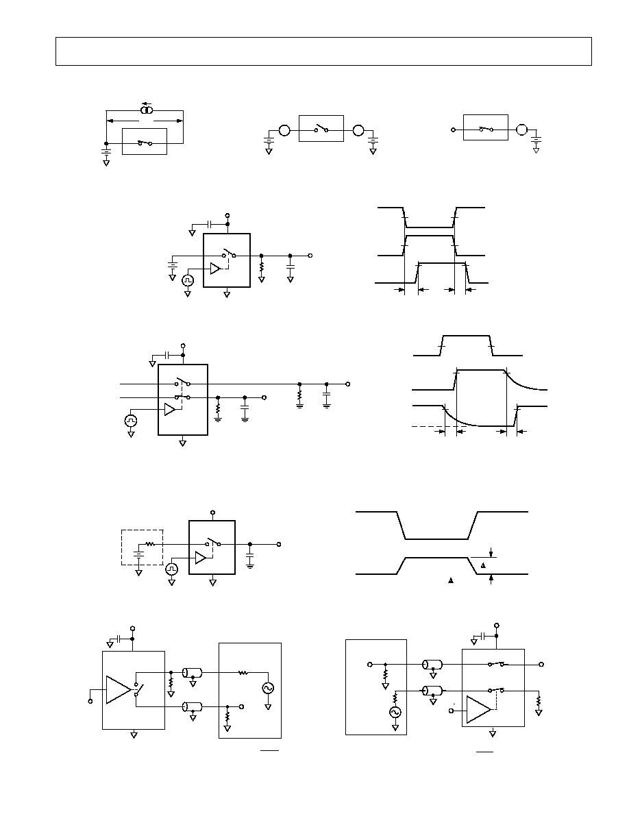
APPLICATIONS
Figure 1 illustrates a photodetector circuit with programmable
gain. An AD820 is used as the output operational amplifier.
With the resistor values shown in the circuit, and using different
combinations of the switches, gain in the range of 2 to 16 can
be achieved.
5V
2.5V
R3
510k
C1
V
OUT
GND
D1
S1
D1
GAIN RANGE 2 TO 16
5V
AD820
S2
D2
S3
D3
S4
D4
(LSB) IN1
IN2
IN3
(MSB) IN4
R4
240k
R5
240k
R6
120k
R7
120k
R8
120k
R9
120k
R10
120k
R1
33k
R2
510k
2.5V
Figure 1. Photodetector Circuit with Programmable Gain
REV. A
ADG781/ADG782/ADG783
7
Test Circuits
I
DS
V1
S
D
V
S
R
ON
= V1/I
DS
Test Circuit 1. On Resistance
V
D
I
S
(OFF)
I
D
(OFF)
S
D
V
S
A
A
Test Circuit 2. Off Leakage
0.1 F
V
S
IN
S
D
V
DD
GND
R
L
300
C
L
35pF
V
OUT
V
DD
ADG781
ADG782
V
IN
V
IN
V
OUT
t
ON
t
OFF
50%
50%
90%
90%
50%
50%
V
S
Test Circuit 4. Switching Times
S1
D1
0.1 F
V
DD
IN1, IN2
V
S1
GND
R
L1
300
C
L1
35pF
V
OUT1
V
S2
V
OUT2
R
L2
300
C
L2
35pF
S2
V
IN
D2
V
DD
ADG783
t
D
t
D
50%
50%
90%
V
IN
V
OUT1
V
OUT2
90%
90%
90%
0V
0V
0V
Test Circuit 5. Break-Before-Make Time Delay, t
D
I
D
(ON)
S
D
A
V
D
NC
NC = NO CONNECT
Test Circuit 3. On Leakage
V
OUT
V
OUT
Q
INJ
= C
L
V
OUT
SW ON
V
IN
SW OFF
S
D
V
DD
IN
R
S
GND
V
S
V
OUT
C
L
1nF
V
DD
Test Circuit 6. Charge Injection
V
S
V
OUT
50
NETWORK
ANALYZER
R
L
50
GND
S
D
V
S
OFF ISOLATION = 20 LOG
V
OUT
0.1 F
V
DD
V
DD
50
V
IN
IN
Test Circuit 7. Off Isolation
CHANNEL-TO-CHANNEL
CROSSTALK = 20 LOG
V
OUT
V
S
GND
S1
D2
S2
NETWORK
ANALYZER
IN
D1
NC
V
OUT
R
L
50
0.1 F
V
DD
V
DD
50
R
L
50
V
S
Test Circuit 8. Channel-to-Channel Crosstalk
REV. A
8
C0237203/02(A)
PRINTED IN U.S.A.
ADG781/ADG782/ADG783
V
S
V
OUT
50
NETWORK
ANALYZER
R
L
50
GND
S
D
0.1 F
V
DD
V
DD
V
IN
IN
V
OUT
WITH SWITCH
V
OUT
WITHOUT SWITCH
INSERTION LOSS = 20 LOG
Test Circuit 9. Bandwidth
OUTLINE DIMENSIONS
Dimensions shown in inches and (mm).
20-Lead CSP
(CP-20)
1
20
5
6
11
16
15
BOTTOM
VIEW
10
0.089 (2.25)
0.083 (2.10) SQ
0.077 (1.95)
0.024 (0.60)
0.017 (0.42)
0.009 (0.24)
0.024 (0.60)
0.017 (0.42)
0.009 (0.24)
0.030 (0.75)
0.024 (0.60)
0.020 (0.50)
0.012 (0.30)
0.009 (0.23)
0.007 (0.18)
0.080 (2.00)
REF
0.010 (0.25)
MIN
0.020 (0.50)
BSC
12
MAX
0.008 (0.20)
REF
0.028 (0.70) MAX
0.026 (0.65) NOM
0.002 (0.05)
0.0004 (0.01)
0.0 (0.0)
0.035 (0.90) MAX
0.033 (0.85) NOM
SEATING
PLANE
CONTROLLING DIMENSIONS ARE IN MILLIMETERS
PIN 1
INDICATOR
TOP
VIEW
0.148 (3.75)
BSC SQ
0.157 (4.0)
BSC SQ
Revision History
Location
Page
Data Sheet changed from REV. 0 to REV. A.
Edits to Typical Performance Characteristics . . . . . . . . . . . . . . . . . . . . . . . . . . . . . . . . . . . . . . . . . . . . . . . . . . . . . . . . . . . . . . . . 56
Changes to OUTLINE DIMENSIONS drawing . . . . . . . . . . . . . . . . . . . . . . . . . . . . . . . . . . . . . . . . . . . . . . . . . . . . . . . . . . . . . . . . 8
Document Outline
- Specifications
- Pinout
- Package drawings
- Ordering Guide
- Features
- Product Description
- Absolute Maximum Ratings
- Functional Block Diagram
- Typical Characteristics
- CAUTION
- TERMINOLOGY
- APPLICATIONS
- DIAGRAMS
- Photodetector Circuit with Programmable Gain
- Test Circuit 1. On Resistance
- Test Circuit 2. Off Leakage
- Test Circuit 3. On Leakage
- Test Circuit 4. Switching Times
- Test Circuit 5. Break-Before-Make Time Delay, tD
- Test Circuit 6. Charge Injection
- Test Circuit 7. Off Isolation
- Test Circuit 8. Channel-to-Channel Crosstalk
- Test Circuit 9. Bandwidth