 | ÐлекÑÑоннÑй компоненÑ: ADG820 | СкаÑаÑÑ:  PDF PDF  ZIP ZIP |
Äîêóìåíòàöèÿ è îïèñàíèÿ www.docs.chipfind.ru
REV. 0
Information furnished by Analog Devices is believed to be accurate and
reliable. However, no responsibility is assumed by Analog Devices for its
use, nor for any infringements of patents or other rights of third parties that
may result from its use. No license is granted by implication or otherwise
under any patent or patent rights of Analog Devices.
a
ADG819/ADG820
One Technology Way, P.O. Box 9106, Norwood, MA 02062-9106, U.S.A.
Tel: 781/329-4700
www.analog.com
Fax: 781/326-8703
© Analog Devices, Inc., 2002
0.5
CMOS
1.8 V to 5.5 V 2:1 Mux/SPDT Switches
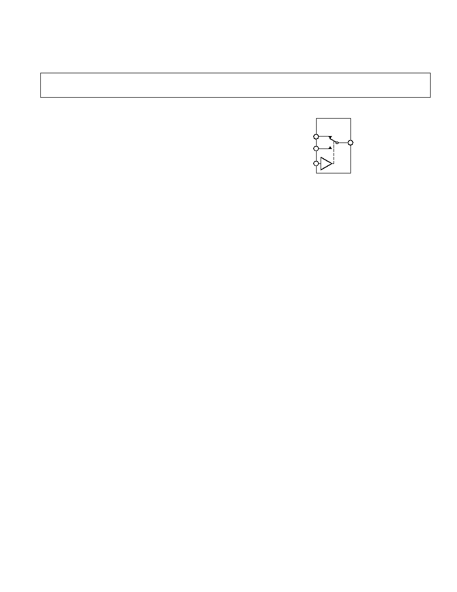
FUNCTIONAL BLOCK DIAGRAM
ADG819/
ADG820
IN
S1
S2
D
SWITCHES SHOWN
FOR A LOGIC "1" INPUT
FEATURES
Low On Resistance 0.8 Max at 125 C
0.25 Max On Resistance Flatness
1.8 V to 5.5 V Single Supply
200 mA Current Carrying Capability
Automotive Temperature Range: 40 C to +125 C
Rail-to-Rail Operation
6-Lead SOT-23 Package, 8-Lead SOIC Package, and
6-Bump MicroCSP (Micro Chip Scale Package) ADG819
Fast Switching Times
Typical Power Consumption (<0.01 W)
TTL-/CMOS-Compatible Inputs
Pin Compatible with the ADG719 (ADG819)
APPLICATIONS
Power Routing
Battery-Powered Systems
Communication Systems
Data Acquisition Systems
Cellular Phones
Modems
PCMCIA Cards
Hard Drives
Relay Replacement
GENERAL DESCRIPTION
The ADG819 and the ADG820 are monolithic, CMOS, SPDT
(single-pole, double-throw) switches. These switches are designed
on a submicron process that provides low power dissipation yet
gives high switching speed, low On resistance, and low leakage
currents.
Low power consumption and an operating supply range of 1.8 V
to 5.5 V make the ADG819 and ADG820 ideal for battery-pow-
ered, portable instruments.
Each switch of the ADG819 and the ADG820 conducts equally
well in both directions when on. The ADG819 exhibits break-
before-make switching action, thus preventing momentary shorting
when switching channels. The ADG820 exhibits make-before-
break action.
The ADG819 and the ADG820 are available in a 6-lead SOT-23
package and an 8-lead
µSOIC package. The ADG819 is also
available in a 2
× 3 bump 1.14 mm × 2.18 mm MicroCSP
package. This chip occupies only a 1.14 mm
× 2.18 mm area,
making it the ideal candidate for space-constrained applications.
PRODUCT HIGHLIGHTS
1. Very low ON resistance, 0.5
typical
2. 1.8 V to 5.5 V single-supply operation
3. High current carrying capability
4. Tiny 6-lead SOT-23 package, 8-lead
µSOIC package,
and 2
× 3 bump 1.14 mm × 2.18 mm MicroCSP package
(ADG819 only)

REV. 0
2
ADG819/ADG820SPECIFICATIONS
1
(V
DD
= 5 V
10%, GND = 0 V.)
40 C to 40 C to
Parameter
25 C
+85 C
+125 C
2
Unit
Test Conditions/Comments
ANALOG SWITCH
Analog Signal Range
0 V to V
DD
V
ON Resistance (R
ON
)
0.5
typ
V
S
= 0 V to V
DD
, I
S
= 100 mA;
0.6
0.7
0.8
max
Test Circuit 1
ON Resistance Match Between
Channels (
R
ON
)
0.06
typ
V
S
= 0 V to V
DD
, I
S
= 100 mA
0.08
0.1
0.12
max
ON Resistance Flatness (R
FLAT(ON)
)
0.1
typ
V
S
= 0 V to V
DD
, I
S
= 100 mA
0.17
0.2
0.25
max
LEAKAGE CURRENTS
V
DD
= 5.5 V
Source OFF Leakage I
S
(OFF)
±0.01
nA typ
V
S
= 4.5 V/1 V, V
D
= 1 V/4.5 V;
±0.25
±3
±10
nA max
Test Circuit 2
Channel ON Leakage I
D
, I
S
(ON)
±0.01
nA typ
V
S
= V
D
= 1 V, or V
S
= V
D
= 4.5 V;
±0.25
±3
±25
nA max
Test Circuit 3
DIGITAL INPUTS
Input High Voltage, V
INH
2.0
V min
Input Low Voltage, V
INL
0.8
V max
Input Current
I
INL
or I
INH
0.005
µA typ
V
IN
= V
INL
or V
INH
±0.1
µA max
C
IN,
Digital Input Capacitance
5
pF typ
DYNAMIC CHARACTERISTICS
3
ADG819
t
ON
35
ns typ
R
L
= 50
, C
L
= 35 pF,
45
50
55
ns max
V
S
= 3 V; Test Circuit 4
t
OFF
10
ns typ
R
L
= 50
, C
L
= 35 pF,
16
18
21
ns max
V
S
= 3 V; Test Circuit 4
Break-Before-Make Time Delay, t
BBM
5
ns typ
R
L
= 50
, C
L
= 35 pF,
1
ns min
V
S1
= V
S2
= 3 V; Test Circuit 5
ADG820
t
ON
10
ns typ
R
L
= 50
, C
L
= 35 pF,
18
20
22
ns max
V
S
= 3 V; Test Circuit 4
t
OFF
26
ns typ
R
L
= 50
, C
L
= 35 pF,
40
45
50
ns max
V
S
= 3 V; Test Circuit 4
Make-Before-Break Time Delay, t
MBB
15
ns typ
R
L
= 50
, C
L
= 35 pF,
1
ns min
V
S
= 0 V; Test Circuit 6
Charge Injection
20
pC typ
V
S
= 2.5 V, R
S
= 0
, C
L
= 1 nF;
Test Circuit 7
Off Isolation
71
dB typ
R
L
= 50
, C
L
= 5 pF, f = 100 kHz;
Test Circuit 8
Channel-to-Channel Crosstalk
72
dB typ
R
L
= 50
, C
L
= 5 pF, f = 100 kHz;
Test Circuit 10
Bandwidth 3 dB
17
MHz typ
R
L
= 50
, C
L
= 5 pF; Test Circuit 9
C
S
(OFF)
80
pF typ
f = 1 MHz
C
D,
C
S
(ON)
300
pF typ
f = 1 MHz
POWER REQUIREMENTS
V
DD
= 5.5 V
Digital Inputs = 0 V or 5.5 V
I
DD
0.001
µA typ
1.0
2.0
µA max
NOTES
1
Temperature range is as follows: 40
°C to +125°C.
2
ON resistance parameters tested with I
S
= 10 mA.
3
Guaranteed by design, not subject to production test.
Specifications subject to change without notice.

REV. 0
3
ADG819/ADG820
SPECIFICATIONS
1
(V
DD
= 2.7 V to 3.6 V, GND = 0 V.)
40 C to 40 C to
Parameter
25 C
+85 C
+125 C
2
Unit
Test Conditions/Comments
ANALOG SWITCH
Analog Signal Range
0 V to V
DD
V
ON Resistance (R
ON
)
0.7
typ
V
S
= 0 V to V
DD
, I
S
= 100 mA;
1.4
1.5
1.6
max
Test Circuit 1
ON Resistance Match Between
Channels (
R
ON
)
0.06
typ
V
S
= 0 V to V
DD
, I
S
= 100 mA
0.13
0.13
max
ON Resistance Flatness (R
FLAT(ON)
)
0.25
typ
V
S
= 0 V to V
DD
, I
S
= 100 mA
LEAKAGE CURRENTS
V
DD
= 3.6 V
Source OFF Leakage I
S
(OFF)
±0.01
nA typ
V
S
= 3.3 V/1 V, V
D
= 1 V/3.3 V;
±0.25
±3
±10
nA max
Test Circuit 2
Channel ON Leakage I
D
, I
S
(ON)
±0.01
nA typ
V
S
= V
D
= 1 V, or V
S
= V
D
= 3.3 V;
±0.25
±3
±25
nA max
Test Circuit 3
DIGITAL INPUTS
Input High Voltage, V
INH
2.0
V min
Input Low Voltage, V
INL
0.8
V max
Input Current
I
INL
or I
INH
0.005
µA typ
V
IN
= V
INL
or V
INH
±0.1
µA max
C
IN,
Digital Input Capacitance
5
pF typ
DYNAMIC CHARACTERISTICS
3
ADG819
t
ON
40
ns typ
R
L
= 50
, C
L
= 35 pF,
60
65
70
ns max
V
S
= 1.5 V; Test Circuit 4
t
OFF
10
ns typ
R
L
= 50
, C
L
= 35 pF,
16
18
21
ns max
V
S
= 1.5 V; Test Circuit
Break-Before-Make Time Delay, t
BBM
40
ns typ
R
L
= 50
, C
L
= 35 pF,
1
ns min
V
S1
= V
S2
= 1.5 V; Test Circuit 5
ADG820
t
ON
20
ns typ
R
L
= 50
, C
L
= 35 pF,
35
40
45
ns max
V
S
= 1.5 V; Test Circuit 4
t
OFF
30
ns typ
R
L
= 50
, C
L
= 35 pF,
45
50
55
ns max
V
S
= 1.5 V; Test Circuit 4
Make-Before-Break Time Delay, t
MBB
10
ns typ
R
L
= 50
, C
L
= 35 pF,
1
ns min
V
S
= 1.5 V; Test Circuit 6
Charge Injection
10
pC typ
V
S
= 1.5 V, R
S
= 0
, C
L
= 1 nF;
Test Circuit 7
Off Isolation
71
dB typ
R
L
= 50
, C
L
= 5 pF, f = 100 kHz;
Test Circuit 8
Channel-to-Channel Crosstalk
72
dB typ
R
L
= 50
, C
L
= 5 pF, f = 100 kHz;
Test Circuit 10
Bandwidth 3 dB
17
MHz typ
R
L
= 50
, C
L
= 5 pF; Test Circuit 9
C
S
(OFF)
80
pF typ
f = 1 MHz
C
D
, C
S
(ON)
300
pF typ
f = 1 MHz
POWER REQUIREMENTS
V
DD
= 3.6 V
Digital Inputs = 0 V or 3.6 V
I
DD
0.001
µA typ
1.0
2.0
µA max
NOTES
1
Temperature range is as follows: 40
°C to +125°C.
2
ON resistance parameters tested with I
S
= 10 mA.
3
Guaranteed by design, not subject to production test.
Specifications subject to change without notice.
REV. 0
ADG819/ADG820
4
ABSOLUTE MAXIMUM RATINGS
1
(T
A
= 25
°C, unless otherwise noted.)
V
DD
to GND . . . . . . . . . . . . . . . . . . . . . . . . . . 0.3 V to +7 V
Analog Inputs
2
. . . . . . . . . . . . . . . . . 0.3 V to V
DD
+ 0.3 V or
. . . . . . . . . . . . . . . . . . . . . . . 30 mA, Whichever Occurs First
Digital Inputs
2
. . . . . . . . . . . . . . . . . 0.3 V to V
DD
+ 0.3 V or
. . . . . . . . . . . . . . . . . . . . . . . 30 mA, Whichever Occurs First
Peak Current, S or D . . . . . . . . . . . . . . . . . . . . . . . . . 400 mA
. . . . . . . . . . . . . . . . (Pulsed at 1 ms, 10% Duty Cycle Max)
Continuous Current, S or D . . . . . . . . . . . . . . . . . . . 200 mA
Operating Temperature Range
Industrial . . . . . . . . . . . . . . . . . . . . . . . . . . . 40
°C to +85°C
Automotive . . . . . . . . . . . . . . . . . . . . . . . . 40
°C to +125°C
Storage Temperature Range . . . . . . . . . . . . 65
°C to +150°C
Junction Temperature . . . . . . . . . . . . . . . . . . . . . . . . . 150
°C
µSOIC Package
JA
Thermal Impedance . . . . . . . . . . . . . . . . . . . . . 206
°C/W
JC
Thermal Impedance . . . . . . . . . . . . . . . . . . . . . . 44
°C/W
SOT-23 Package (4-Layer Board)
JA
Thermal Impedance . . . . . . . . . . . . . . . . . . . . . 119
°C/W
MicroCSP Package
JA
Thermal Impedance . . . . . . . . . . . . . . . . . . . . . . . . TBD
Lead Temperature, Soldering (10 sec) . . . . . . . . . . . . 300
°C
IR Reflow, Peak Temperature (<20 sec) . . . . . . . . . . . 235
°C
NOTES
1
Stresses above those listed under Absolute Maximum Ratings may cause perma-
nent damage to the device. This is a stress rating only; functional operation of the
device at these or any other conditions above those listed in the operational
sections of this specification is not implied. Exposure to absolute maximum rating
conditions for extended periods may affect device reliability. Only one absolute
maximum rating may be applied at any one time.
2
Overvoltages at IN, S, or D will be clamped by internal diodes. Current should be
limited to the maximum ratings given.
Table I. Truth Table for the ADG819/ADG820
IN
Switch S1
Switch S2
0
ON
OFF
1
OFF
ON
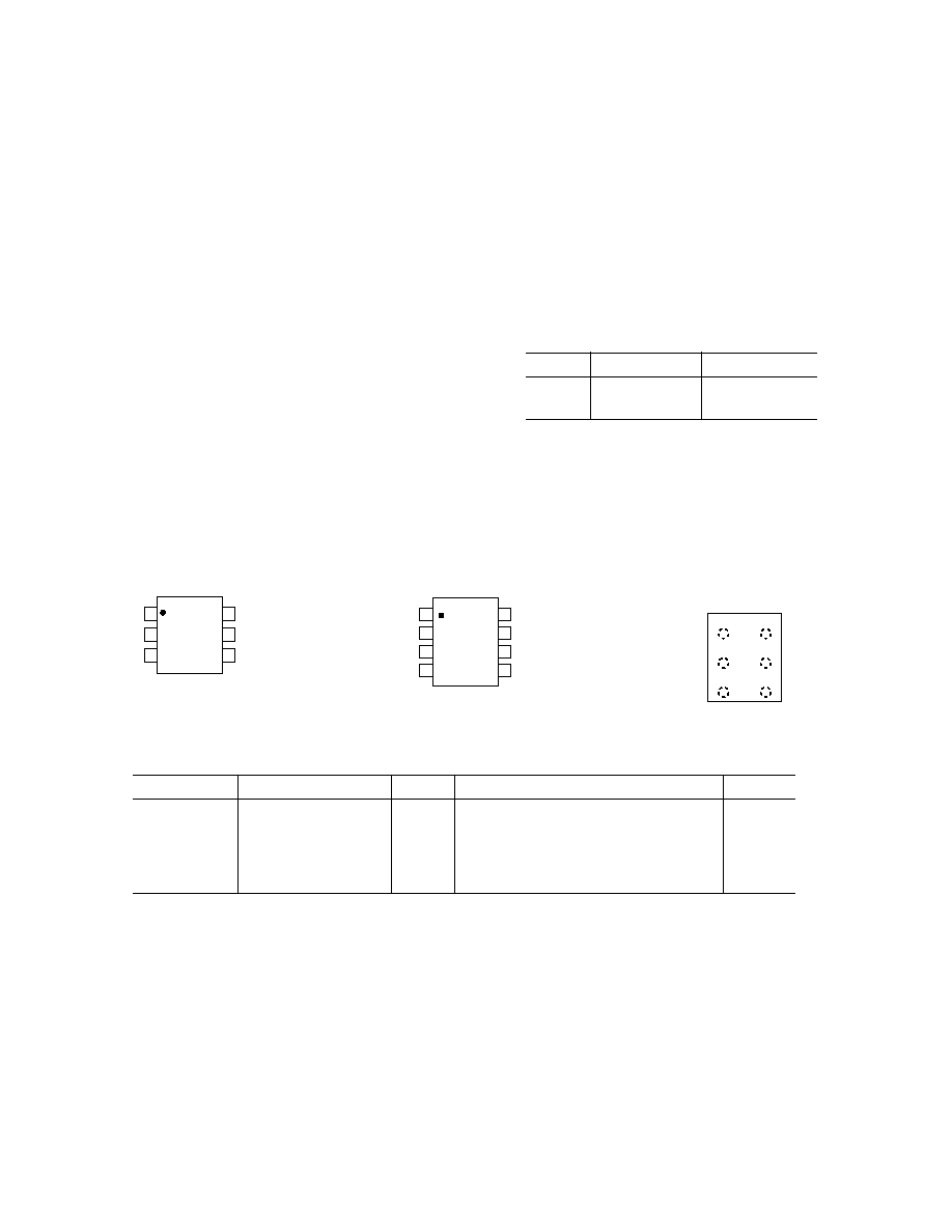
PIN CONFIGURATIONS
6-Lead SOT-23
(RT-6)
TOP VIEW
(Not to Scale)
6
5
4
1
2
3
IN
S2
ADG819/
ADG820
V
DD
GND
D
S1
8-Lead
µSOIC
(RM-8)
TOP VIEW
(Not to Scale)
8
7
6
5
1
2
3
4
NC = NO CONNECT
D
S2
ADG819/
ADG820
S1
V
DD
GND
NC
IN
NC
2 3 MicroCSP
S2
IN
S1
V
DD
D
GND
ADG819 ONLY
TOP VIEW
(BUMPS AT THE BOTTOM)
NOT TO SCALE
1
2
3
6
5
4
ORDERING GUIDE
Model Option
Temperature Range
Brand
1
Package Description
Package
ADG819BRM
40
°C to +125°C
SNB
µSOIC (MicroSmall Outline IC)
RM-8
ADG819BRT
40
°C to +125°C
SNB
SOT-23 (Plastic Surface-Mount)
RT-6
2
ADG819BCB
40
°C to +85°C
SNB
MicroCSP (Micro Chip Scale Package)
CB-6
2
ADG820BRM
40
°C to +125°C
SPB
µSOIC (MicroSmall Outline IC)
RM-8
ADG820BRT
40
°C to +125°C
SPB
SOT-23 (Plastic Surface-Mount)
RT-6
2
NOTES
1
Branding on these packages is limited to three characters due to space constraints.
2
Contact factory for availability.
REV. 0
ADG819/ADG820
5
CAUTION
ESD (electrostatic discharge) sensitive device. Electrostatic charges as high as 4000 V readily accumulate
on the human body and test equipment and can discharge without detection. Although the ADG819/
ADG820 features proprietary ESD protection circuitry, permanent damage may occur on devices
subjected to high energy electrostatic discharges. Therefore, proper ESD precautions are recommended
to avoid performance degradation or loss of functionality.
WARNING!
ESD SENSITIVE DEVICE
TERMINOLOGY
V
DD
Most Positive Power Supply Potential
GND
Ground (0 V) Reference
I
DD
Positive Supply Current
S
Source Terminal. May be an input or output.
D
Drain Terminal. May be an input or output.
IN
Logic Control Input
R
ON
Ohmic Resistance between D and S
R
ON
ON Resistance Match between Any Two Channels, i.e., R
ON
max R
ON
min
R
FLAT(ON)
Flatness is defined as the difference between the maximum and minimum value of ON resistance as
measured over the specified analog signal range.
I
S
(OFF)
Source Leakage Current with the Switch OFF
I
D
, I
S
(ON)
Channel Leakage Current with the Switch ON
V
D
(V
S
)
Analog Voltage on Terminals D, S
V
INL
Maximum Input Voltage for Logic "0"
V
INH
Minimum Input Voltage for Logic "1"
I
INL
(I
INH
)
Input Current of the Digital Input
C
S
(OFF)
OFF Switch Source Capacitance
C
D
, C
S
(ON)
ON Switch Capacitance
t
ON
Delay between applying the digital control input and the output switching ON.
t
OFF
Delay between applying the digital control input and the output switching OFF.
t
BBM
OFF time or ON time measured between the 90% points of both switches when switching
from one address state to another.
t
MBB
ON time measured between the 80% points of both switches when switching from one
address state to another.
Charge Injection
A measure of the glitch impulse transferred from the digital input to the analog output during switching.
Crosstalk
A measure of unwanted signal coupled through from one channel to another as a result of parasitic
capacitance.
OFF Isolation
A measure of unwanted signal coupling through an OFF switch.
Bandwidth
Frequency at which the output is attenuated by 3 dB.
ON Response
Frequency Response of the ON Switch
Insertion Loss
Loss due to the ON Resistance of the Switch
REV. 0
ADG819/ADG820
6
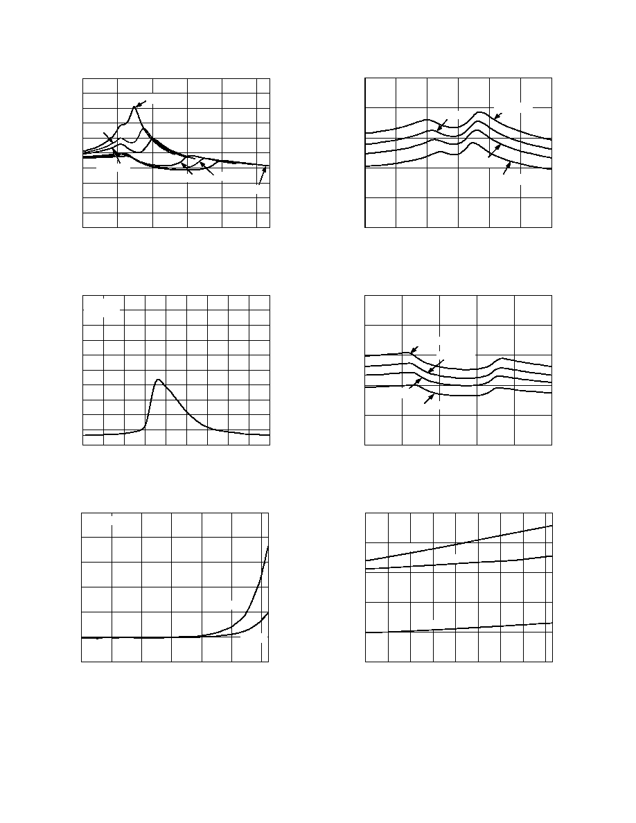
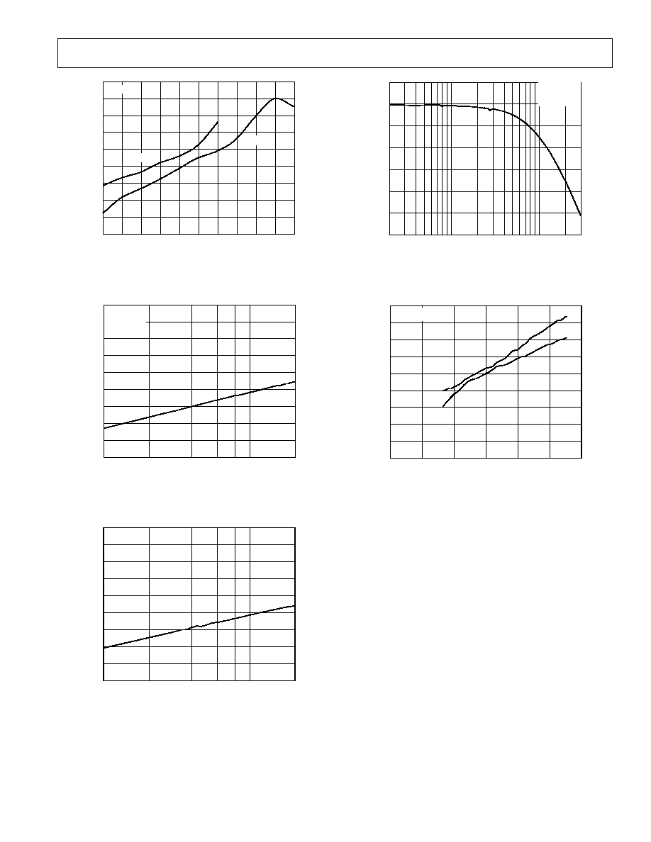
Typical Performance Characteristics
V
D
, V
S
V
1.0
0
1
2
3
4
5
ON RESISTANCE
0.8
0.6
0.4
0.2
0
0.9
0.7
0.5
0.3
0.1
T
A
= 25 C
V
DD
= 3V
V
DD
= 5.5V
V
DD
= 5V
V
DD
= 4.5V
V
DD
= 2.7V
V
DD
= 3.3V
TPC 1. ON Resistance vs. V
D
(V
S
)
V
D
, V
S
V
10
0
0.2
0.6
1.0
1.2
1.6
ON RESISTANCE
8
6
4
2
0
9
7
5
3
1
T
A
= 25 C
V
DD
= 1.8V
0.4
0.8
1.4
1.8
TPC 2. ON Resistance vs. V
D
(V
S
)
TEMPERATURE C
10
0
60
LEAKAGE CURRENTS nA
6
4
2
0
2
20
40
100
120
80
8
I
S
(OFF)
I
D
,
I
S
(ON)
V
DD
= 3V, 5V
TPC 3. Leakage Currents vs. Temperatures
V
D
, V
S
V
1.0
0
1.5
ON RESISTANCE
0.8
0.6
0.4
0.2
0
V
DD
= 3V
0.5
1.0
2.5
3.0
T
A
= +85 C
T
A
= +125 C
T
A
= +25 C
T
A
= 40 C
2.0
TPC 4. ON Resistance vs. V
D
(V
S
) for Different Temperatures
V
D
, V
S
V
1.0
0
3
ON RESISTANCE
0.8
0.6
0.4
0.2
0
V
DD
= 5V
1
2
4
5
T
A
= +85 C
T
A
= +125 C
T
A
= +25 C
T
A
= 40 C
TPC 5. ON Resistance vs. V
D
(V
S
) for Different Temperatures
TEMPERATURE C
50
40
20
TIME ns
40
30
20
10
0
20
0
80
120
40
t
ON
60
100
t
OFF
V
DD
= 3V, 5V
V
DD
= 5V
V
DD
= 3V
TPC 6. t
ON
/t
OFF
Times vs. Temperature (ADG819)
REV. 0
ADG819/ADG820
7
V
S
V
250
0
3.0
CHARGE INJECTION pC
150
0
100
150
200
V
DD
= 3V
1.0
2.0
4.0
5.0
T
A
= 25 C
200
100
50
50
2.5
0.5
1.5
3.5
4.5
V
DD
= 5V
TPC 7. Charge Injection vs. Source Voltage
FREQUENCY MHz
0
0.1
ATTENUATION dB
20
50
70
80
90
2
10
30
40
60
1
V
DD
= 5V, 3V
T
A
= 25 C
TPC 8. OFF Isolation vs. Frequency
FREQUENCY MHz
0
0.1
ATTENUATION dB
20
50
70
80
90
2
10
30
40
60
1
TPC 9. Crosstalk vs. Frequency
FREQUENCY MHz
0
0.2
ATTENUATION dB
2
5
6
10
1
3
4
1
1
30
V
DD
= 3V, 5V
T
A
= 25 C
TPC 10. ON Response vs. Frequency
V
DD
V
1.6
0
1.2
0.6
0.4
2
1.4
1.0
0.8
1
1.8
3
T
A
= 25 C
0.2
0
LOGIC THRESHOLD VOLTAGE V
4
5
6
RISING
FALLING
TPC 11. Logic Threshold vs. Supply Voltage
REV. 0
ADG819/ADG820
8
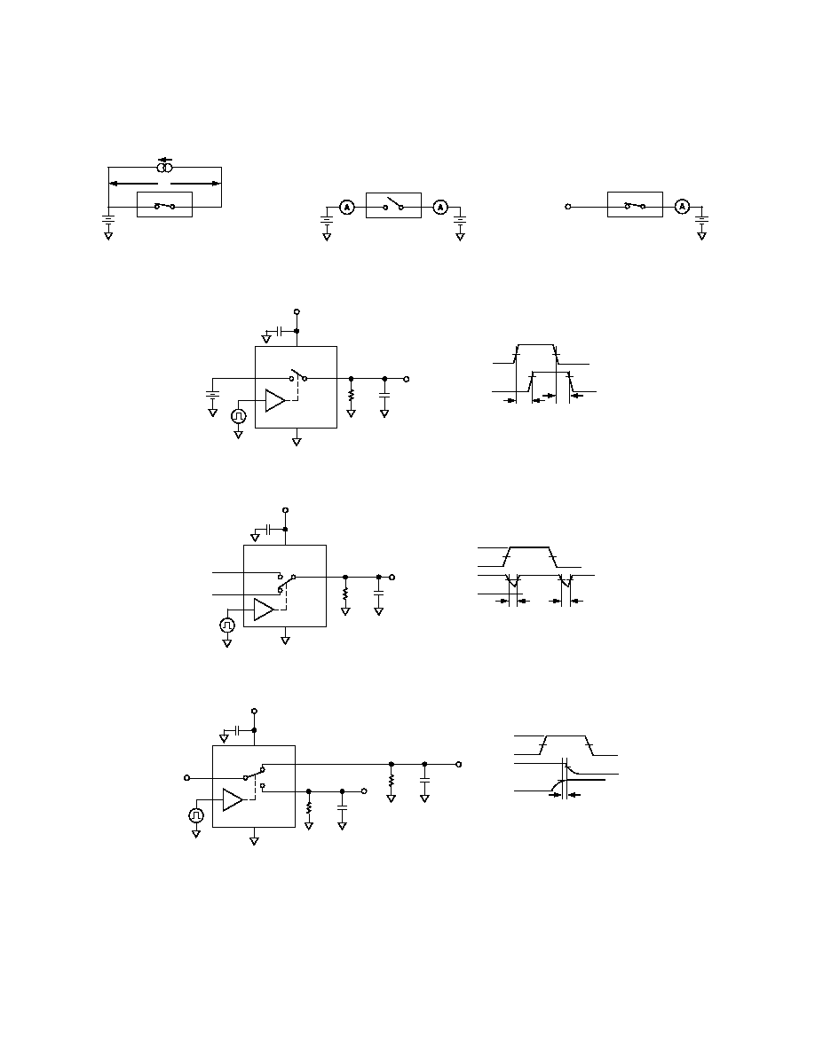
Test Circuits
S
D
V1
V
S
R
ON
= V1 / I
OS
I
DS
Test Circuit 1. ON Resistance
S
D
V
S
V
D
I
D
(OFF)
I
S
(OFF)
Test Circuit 2. OFF Leakage
S
D
V
D
I
D
(ON)
NC
NC = NO CONNECT
Test Circuit 3. ON Leakage
V
S
R
L
50
C
L
35pF
IN
GND
V
DD
V
DD
0.1 F
V
OUT
V
IN
50%
90%
90%
t
ON
t
OFF
50%
Test Circuit 4. Switching Times
V
S2
R
L
50
C
L
35pF
V
OUT
IN
GND
V
DD
V
DD
0.1 F
S2
S1
V
S1
V
IN
V
OUT
V
IN
0V
0V
50%
90%
90%
t
BBM
t
BBM
50%
D
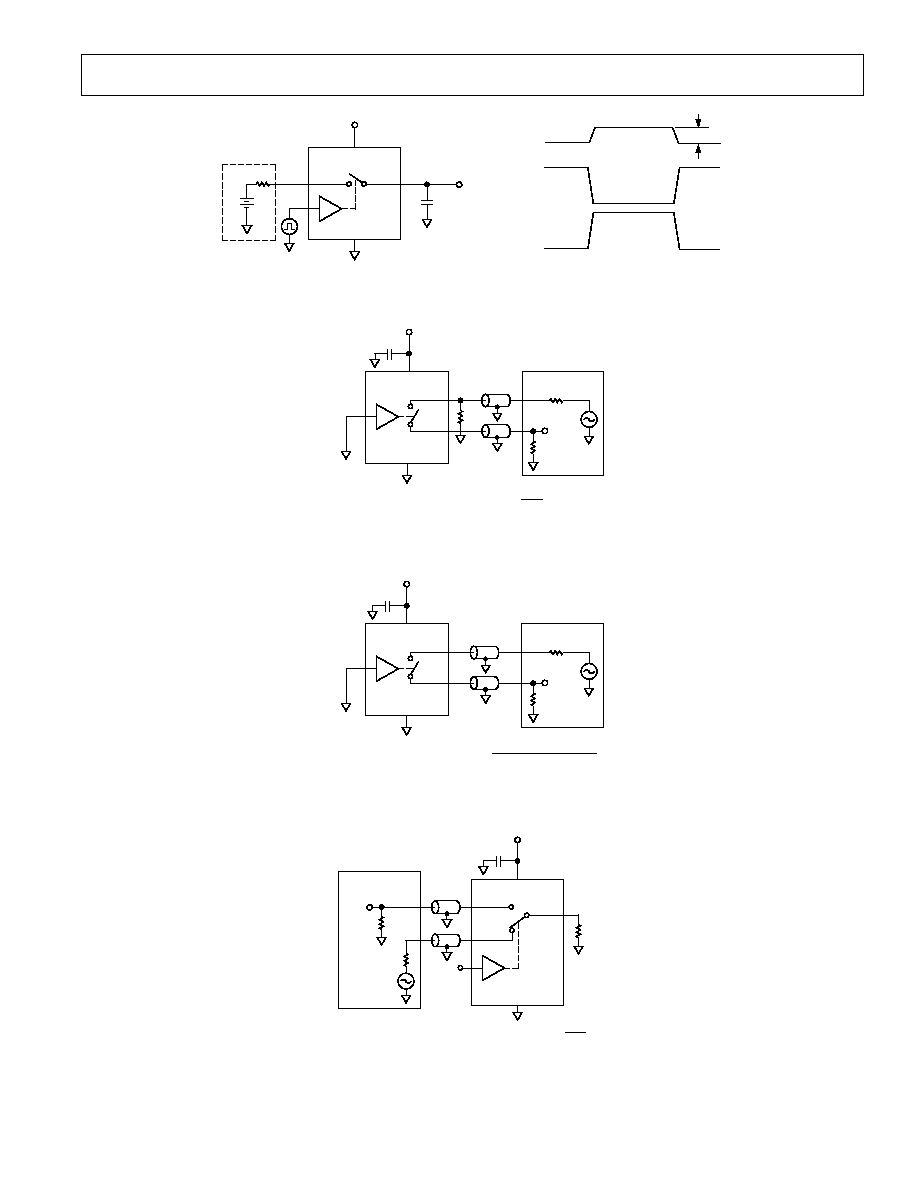
Test Circuit 5. Break-Before-Make Time Delay, t
BBM
(ADG819 Only)
R
L2
300
C
L2
35pF
V
S2
IN
GND
V
DD
V
DD
0.1 F
V
D
R
L1
300
C
L1
35pF
V
S1
V
IN
V
IN
0V
50%
90%
80% V
D
80% V
D
50%
V
S1
V
S2
t
MBB
Test Circuit 6. Make-Before-Break Time Delay, t
MBB
(ADG820 Only)
REV. 0
ADG819/ADG820
9
V
S
C
L
1nF
IN
GND
V
DD
V
DD
V
OUT
SW OFF
SW OFF
SW OFF
SW OFF
SW ON
SW ON
Q
INJ
= C
L
V
OUT
V
OUT
V
IN
V
IN
R
S
V
OUT
Test Circuit 7. Charge Injection
IN
GND
V
DD
V
DD
0.1 F
50
V
IN
S
D
NETWORK
ANALYZER
V
OUT
R
L
50
V
S
50
OFF ISOLATION = 20 LOG
V
OUT
V
S
Test Circuit 8. OFF Isolation
IN
GND
V
DD
V
DD
0.1 F
V
IN
S
D
NETWORK
ANALYZER
V
OUT
R
L
50
V
S
50
INSERTION LOSS = 20 LOG
V
OUT
WITH SWITCH
V
OUT
WITHOUT SWITCH
Test Circuit 9. Bandwidth
GND
V
DD
0.1 F
S2
S1
D
IN
NETWORK
ANALYZER
V
OUT
R
L
50
V
S
R
50
CHANNEL-TO-CHANNEL CROSSTALK = 20 LOG
V
OUT
V
S
V
DD
50
Test Circuit 10. Channel-to-Channel Crosstalk
REV. 0
ADG819/ADG820
10
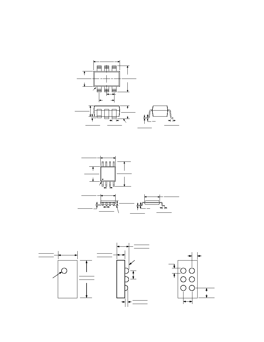
OUTLINE DIMENSIONS
6-Lead Plastic Surface-Mount Package
(RT-6)
Dimensions shown in inches and (mm)
1
3
4
5
2
6
0.1220 (3.10)
0.1063 (2.70)
PIN 1
0.0709 (1.80)
0.0591 (1.50)
0.1181 (3.00)
0.0984 (2.50)
0.0748
(1.90)
BSC
0.0374 (0.95)
BSC
0.0091 (0.23)
0.0031 (0.08)
0.0217 (0.55)
0.0138 (0.35)
10
0
0.0197 (0.50)
0.0098 (0.25)
0.0059 (0.15)
0.0000 (0.00)
0.0512 (1.30)
0.0354 (0.90)
SEATING
PLANE
0.0571 (1.45)
0.0354 (0.90)
COPLANARITY
8-Lead SOIC Package
(RM-8)
Dimensions shown in inches and (mm)
0.0110 (0.28)
0.0031 (0.08)
0.0280 (0.71)
0.0161 (0.41)
33
27
0.1201 (3.05)
0.1118 (2.84)
8
5
4
1
0.1220 (3.10)
0.1142 (2.90)
0.1988 (5.05)
0.1870 (4.75)
PIN 1
0.0256 (0.65) BSC
0.1220 (3.10)
0.1142 (2.90)
SEATING
PLANE
0.0059 (0.15)
0.0020 (0.05)
0.0181 (0.46)
0.0079 (0.20)
0.0429 (1.09)
0.0370 (0.94)
0.1201 (3.05)
0.1118 (2.84)
COPLANARITY
2
× 3 Array for MicroCSP
(CB-6)
Dimensions shown in millimeters and (inches)
PIN 1
IDENTIFIER
SEATING
PLANE
1.34 (0.0528)
1.14 (0.0449)
0.94 (0.0370)
0.67 (0.0264)
0.57 (0.0224)
0.47 (0.0185)
0.24 (0.0094)
0.22 (0.0087)
0.20 (0.0079)
0.50 (0.0860)
0.50 (0.0197)
BALL PITCH
COPLANARITY
0.32 (0.0126)
NOM
0.32 (0.0126)
0.44 (0.0173)
0.36 (0.0142)
0.28 (0.0110)
2.38 (0.0937)
2.18 (0.0858)
1.98 (0.0780)
0.59 (0.0232)
CONTROLLING DIMENSIONS ARE IN MILLIMETERS; INCH DIMENSIONS
(IN PARENTHESES) ARE ROUNDED-OFF MILLIMETER EQUIVALENTS FOR
REFERENCE ONLY AND ARE NOT APPROPRIATE FOR USE IN DESIGN

11

12
C0280105/02(0)
PRINTED IN U.S.A.