 | –≠–ª–µ–∫—Ç—Ä–æ–Ω–Ω—ã–π –∫–æ–º–ø–æ–Ω–µ–Ω—Ç: ADG919 | –°–∫–∞—á–∞—Ç—å:  PDF PDF  ZIP ZIP |

ADG918/ADG919
a
REV. PrC Sept 2002
Information furnished by Analog Devices is believed to be accurate and
reliable. However, no responsibility is assumed by Analog Devices for its
use, nor for any infringements of patents or other rights of third parties
which may result from its use. No license is granted by implication or
otherwise under any patent or patent rights of Analog Devices.
One Technology Way, P.O. Box 9106, Norwood, MA 02062-9106, U.S.A.
Tel: 781/329-4700
www.analog.com
Fax: 781/326-8703
Analog Devices, Inc., 2002
Wideband, 43dB Isolation @ 1GHz,
CMOS 1.65 V to 2.75V, 2:1 Mux/SPDT Switches
Preliminary Technical Data
PRELIMINARY TECHNICAL DATA
FEATURES
Wideband DC to 2GHz
ADG918/ADG919 Absorptive/Reflective Switches
High Off Isolation (43 dB @ 1 GHz)
Low Insertion Loss (1 dB DC to 900 MHz)
Single 1.65 to 2.75 V power supply
CMOS/LVTTL Control Logic
8 Lead MSOP & Tiny 3 x 3mm CSP Packages
Low Power Consumption (5
µµ
µµ
µ
A)
APPLICATIONS
Wireless Communications
General Purpose RF switching
Dual Band Applications
Filter Selection
Antenna Switch
Digital Transceiver Front-End Switch
IF Switching
GENERAL DESCRIPTION
The ADG918/ADG919 are wideband switches using a
CMOS process to provide high isolation and low insertion
loss to 1GHz. The ADG918 is an absorptive switch
having 50 ohm terminated shunt legs, while the ADG919
is a reflective switch. These devices are designed such that
the isolation is high over the DC to 1GHz frequency
range. They have on board CMOS control logic, thus
eliminating the need for external controlling circuitry.
The control inputs are both CMOS and LVTTL
compatible. The low power consumption of these CMOS
devices makes them ideally suited to wireless applications
and general purpose high frequency switching.
FUNCTIONAL BLOCK DIAGRAM
Table 1. Truth Table
Control
Signal Path
0
RF2 to RF Common
1
RF1 to RF Common
Figure 2. Loss vs Frequency
Figure 1. Isolation vs Frequency
RF2
RF1
CONTROL
ADG918
RF COMMON
50
50
RF2
RF1
CONTROL
ADG919
RF COMMON

≠2≠
REV. PrC
ADG918/ADG919≠SPECIFICATIONS
1
(V
DD
= +1.65 V to +2.75 V, GND = 0 V, All specifications T
MIN
to T
MAX
unless otherwise noted)
PRELIMINARY TECHNICAL DATA
B Version
Parameter
Symbol
Conditions
Min
Typ
2
Max
Units
AC ELECTRICAL CHARACTERISTICS
Operating Frequency
DC
2
GHz
Insertion Loss
S
21
, S
12
DC - 100 MHz
0.4
dB
500 MHz
0.65
dB
900 MHz
1.0
dB
Isolation- RF to RF1/RF2
S
21
, S
12
1 MHz
100
dB
100 MHz
55
dB
500 MHz
dB
1000 MHz
43
dB
Isolation - RF1 to RF2
S
21
, S
12
1 MHz
100
dB
100 MHz
55
dB
500 MHz
dB
1000 MHz
30
dB
Return Loss (On Channel)
S
11
, S
22
DC - 100 MHz
26
dB
500 MHz
dB
1000 MHz
23
dB
On switching Time
t
ON
50% Control to 90% RF
5
ns
Off Switching Time
t
OFF
50% Control to 10% RF
4
ns
1 dB Compression
P
-1dB
DC to 1000 MHz
20
dBm
Third Order Intermodulation intercept
IP
3
900MHz, 5dBm
35
dBm
DC ELECTRICAL CHARACTERISTICS
Input High Voltage
V
INH
V
DD
= 2.3 V to 2.75 V
1.7
V
V
INH
V
DD
= 1.65 V to 1.95 V
0.65V
CC
V
Input Low Voltage
V
INL
V
DD
= 2.3 V to 2.75 V
0.7
V
V
INL
V
DD
= 1.65 V to 1.95 V
0.35V
CC
V
Input Leakage Current
I
I
0 V
IN
2.75 V
±1
µA
CAPACITANCE
3
RF1/RF2, RF Port On Capacitance
C
RF
ON
f = 1 MHz
2
pF
Control Input Capacitance
C
IN
f = 1 MHz
2
pF
POWER REQUIREMENTS
V
DD
1.65
2.75
V
Quiescent Power Supply Current
I
DD
Digital Inputs = 0 V or V
DD
1
5
µA
N O T E S
1
Temperature range is as follows: B Version: ≠40∞C to +85∞C.
2
Typical values are at +25∞C unless otherwise stated.
3
Guaranteed by design, not subject to production test.
Specifications subject to change without notice.
ADG918/ADG919
≠3≠
REV. PrC
PRELIMINARY TECHNICAL DATA
ABSOLUTE MAXIMUM RATINGS
1
(T
A
= +25∞C unless otherwise noted)
V
DD
to GND
-0.5 V to +4 V
Inputs
to GND
-0.5 V to V
DD
+ 0.3V
Input Power
TBD dBm
Operating Temperature Range
Industrial (B Version)
≠40∞C to +85∞C
Storage Temperature Range
≠65∞C to +150∞C
Junction Temperature
+150∞C
MSOP Package
JA
Thermal Impedance
206∞C/W
CSP Package
JA
Thermal Impedance
T B D ∞ C / W
Lead Temperature, Soldering (10seconds)
300∞C
IR Reflow, Peak Temperature (<20 seconds)
+235∞C
NOTES
1
Stresses above those listed under "Absolute Maximum Ratings" may cause permanent
damage to the device. This is a stress rating only and functional operation of the device
at these or any other conditions above those listed in the operational sections of this
specification is not implied. Exposure to absolute maximum rating conditions for
extended periods may affect device reliability. Only one absolute maximum rating may
be applied at any one time.
CAUTION
ESD (electrostatic discharge) sensitive device. Electrostatic charges as high as 4000 V readily
accumulate on the human body and test equipment and can discharge without detection.
Although the ADG919 features proprietary ESD protection circuitry, permanent damage may
occur on devices subjected to high energy electrostatic discharges. Therefore, proper ESD
precautions are recommended to avoid performance degradation or loss of functionality.
ORDERING GUIDE
Model
Temperature Range
Package Descriptions
Branding
Package Options
ADG918BRM
≠40∞C to +85∞C
MSOP (Micro Small Outline Package)
RM-8
ADG918BCP
≠40∞C to +85∞C
Chip Scale Package
CP-8
ADG919BRM
≠40∞C to +85∞C
MSOP (Micro Small Outline Package)
RM-8
ADG919BCP
≠40∞C to +85∞C
Chip Scale Package
CP-8
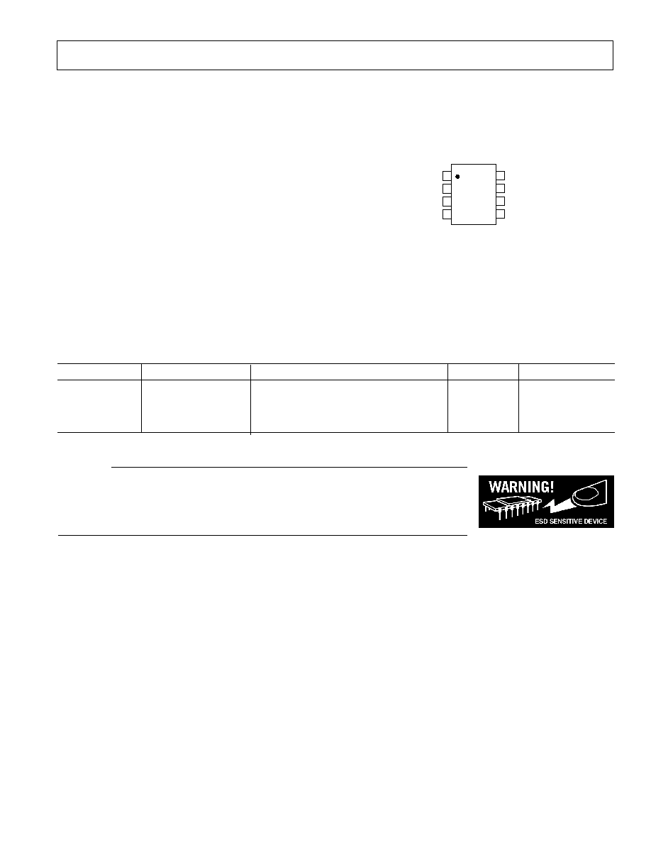
PIN CONFIGURATION
8-Lead MSOP (RM-8)
3x3mm CSP (CP-8)
TOP VIEW
(Not to Scale)
8
7
6
5
1
2
3
4
VDD
CONTROL
GND
RFCommon
ADG918/
ADG919
GND
GND
RF1
RF2
ADG918/ADG919
≠4≠
REV. PrC
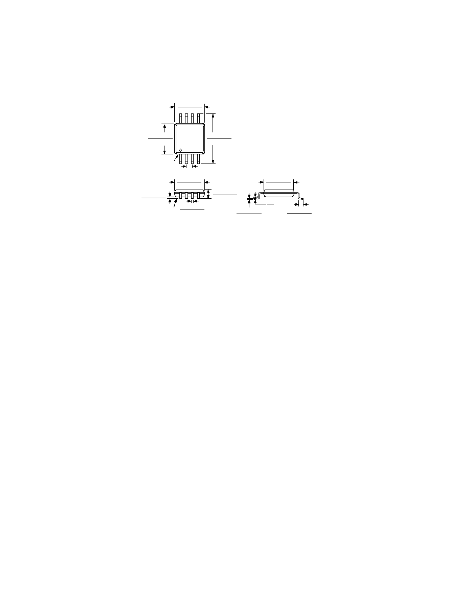
OUTLINE DIMENSIONS
Dimensions shown in inches and (mm).
PRELIMINARY TECHNICAL DATA
M S O P
(RM-8)
8
5
4
1
0.122 (3.10)
0.114 (2.90)
0.199 (5.05)
0.187 (4.75)
PIN 1
0.0256 (0.65) BSC
0.122 (3.10)
0.114 (2.90)
SEATING
PLANE
0.006 (0.15)
0.002 (0.05)
0.018 (0.46)
0.008 (0.20)
0.043 (1.09)
0.037 (0.94)
0.120 (3.05)
0.112 (2.84)
0.011 (0.28)
0.003 (0.08)
0.028 (0.71)
0.016 (0.41)
33
27
0.120 (3.05)
0.112 (2.84)
Chip Scale Package
(CP-8)
3 x 3mm
T B D