 | ÐлекÑÑоннÑй компоненÑ: ADM1485 | СкаÑаÑÑ:  PDF PDF  ZIP ZIP |
Äîêóìåíòàöèÿ è îïèñàíèÿ www.docs.chipfind.ru
REV. A
Information furnished by Analog Devices is believed to be accurate and
reliable. However, no responsibility is assumed by Analog Devices for its
use, nor for any infringements of patents or other rights of third parties
which may result from its use. No license is granted by implication or
otherwise under any patent or patent rights of Analog Devices.
a
+5 V Low Power
EIA RS-485 Transceiver
ADM1485
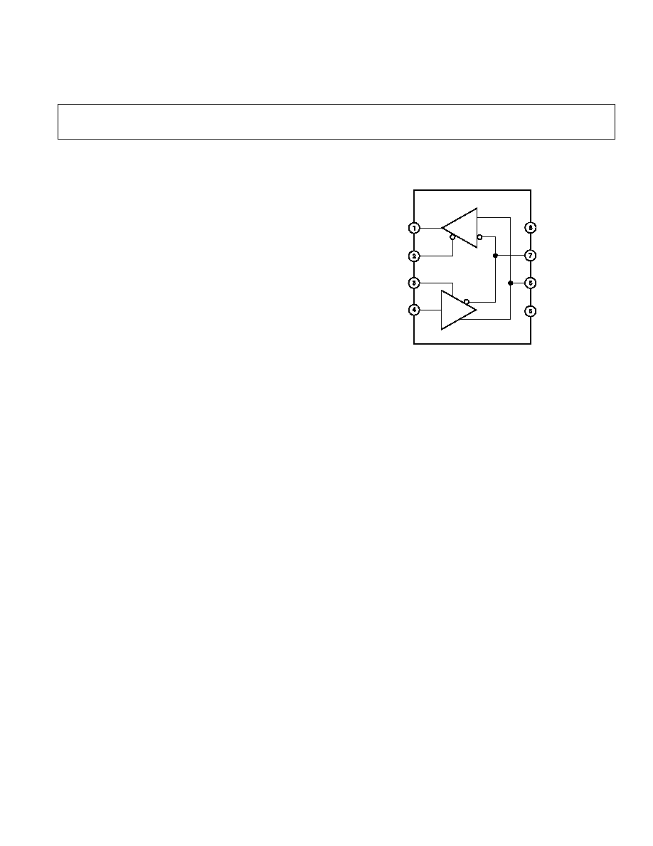
FUNCTIONAL BLOCK DIAGRAM
8-Lead
ADM1485
R
D
RO
RE
DE
DI
V
CC
B
A
GND
FEATURES
Meets EIA RS-485 Standard
30 Mb/s Data Rate
Single +5 V Supply
7 V to +12 V Bus Common-Mode Range
High Speed, Low Power BiCMOS
Thermal Shutdown Protection
Short Circuit Protection
Zero Skew Driver
Driver Propagation Delay: 10 ns
Receiver Propagation Delay: 25 ns
High Z Outputs with Power Off
Superior Upgrade for LTC1485
APPLICATIONS
Low Power RS-485 Systems
DTE-DCE Interface
Packet Switching
Local Area Networks
Data Concentration
Data Multiplexers
Integrated Services Digital Network (ISDN)
GENERAL DESCRIPTION
The ADM1485 is a differential line transceiver suitable for high
speed bidirectional data communication on multipoint bus
transmission lines. It is designed for balanced data transmission
and complies with both EIA Standards RS-485 and RS-422.
The part contains a differential line driver and a differential line
receiver. Both the driver and the receiver may be enabled inde-
pendently. When disabled, the outputs are tristated.
The ADM1485 operates from a single +5 V power supply.
Excessive power dissipation caused by bus contention or by
output shorting is prevented by a thermal shutdown circuit.
This feature forces the driver output into a high impedance state
if during fault conditions a significant temperature increase is
detected in the internal driver circuitry.
Up to 32 transceivers may be connected simultaneously on a
bus, but only one driver should be enabled at any time. It is
important therefore that the remaining disabled drivers do not
load the bus. To ensure this, the ADM1485 driver features high
output impedance when disabled and also when powered down.
This minimizes the loading effect when the transceiver is not
being utilized. The high impedance driver output is maintained
over the entire common-mode voltage range from 7 V to +12 V.
The receiver contains a fail safe feature which results in a logic
high output state if the inputs are unconnected (floating).
The ADM1485 is fabricated on BiCMOS, an advanced mixed
technology process combining low power CMOS with fast
switching bipolar technology. All inputs and outputs contain
protection against ESD; all driver outputs feature high source
and sink current capability. An epitaxial layer is used to guard
against latch-up.
The ADM1485 features extremely fast switching speeds. Mini-
mal driver propagation delays permit transmission at data rates
up to 30 Mbits/s while low skew minimizes EMI interference.
The part is fully specified over the commercial and industrial
temperature range and is available in an 8-lead DIL/SOIC
package.
One Technology Way, P.O. Box 9106, Norwood, MA 02062-9106, U.S.A.
Tel: 781/329-4700
World Wide Web Site: http://www.analog.com
Fax: 781/326-8703
© Analog Devices, Inc., 2000
REV. A
2
ADM1485SPECIFICATIONS
(V
CC
= +5 V 5%. All specifications T
MIN
to T
MAX
unless otherwise noted.)
Parameter
Min
Typ
Max
Unit
Test Conditions/Comments
DRIVER
Differential Output Voltage, V
OD
5.0
V
R =
, Figure 1
2.0
5.0
V
V
CC
= 5 V, R = 50
(RS-422), Figure 1
1.5
5.0
V
R = 27
(RS-485), Figure 1
V
OD3
1.5
5.0
V
V
TST
= 7 V to +12 V, Figure 2
|V
OD
| for Complementary Output States
0.2
V
R = 27
or 50 , Figure 1
Common-Mode Output Voltage V
OC
3
V
R = 27
or 50 , Figure 1
|V
OD
| for Complementary Output States
0.2
V
R = 27
or 50
Output Short Circuit Current (V
OUT
= High)
35
250
mA
7 V
V
O
+12 V
Output Short Circuit Current (V
OUT
= Low)
35
250
mA
7 V
V
O
+12 V
CMOS Input Logic Threshold Low, V
INL
0.8
V
CMOS Input Logic Threshold High, V
INH
2.0
V
Logic Input Current (DE, DI)
±1.0
µA
RECEIVER
Differential Input Threshold Voltage, V
TH
0.2
+0.2
V
7 V
V
CM
+12 V
Input Voltage Hysteresis,
V
TH
70
mV
V
CM
= 0 V
Input Resistance
12
k
7 V
V
CM
+12 V
Input Current (A, B)
+ 1
mA
V
IN
= 12 V
0.8
mA
V
IN
= 7 V
Logic Enable Input Current (
RE)
±1
µA
CMOS Output Voltage Low, V
OL
0.4
V
I
OUT
= +4.0 mA
CMOS Output Voltage High, V
OH
4.0
V
I
OUT
= 4.0 mA
Short Circuit Output Current
7
85
mA
V
OUT
= GND or V
CC
Tristate Output Leakage Current
±1.0
µA
0.4 V
V
OUT
+2.4 V
POWER SUPPLY CURRENT
I
CC
(Outputs Enabled)
1.35
2.2
mA
Outputs Unloaded, Digital Inputs = GND or V
CC
I
CC
(Outputs Disabled)
0.7
1
mA
Outputs Unloaded, Digital Inputs = GND or V
CC
Specifications subject to change without notice.
TIMING SPECIFICATIONS
Parameter
Min
Typ
Max
Unit
Test Conditions/Comments
DRIVER
Propagation Delay Input to Output T
PLH
, T
PHL
2
10
15
ns
R
L
Diff = 54
C
L1
= C
L2
= 100 pF, Figure 3
Driver O/P to
O/P T
SKEW
0
5
ns
R
L
Diff = 54
C
L1
= C
L2
= 100 pF, Figure 3
Driver Rise/Fall Time T
R
, T
F
2
10
ns
R
L
Diff = 54
C
L1
= C
L2
= 100 pF, Figure 3
Driver Enable to Output Valid
10
25
ns
Driver Disable Timing
10
25
ns
RECEIVER
Propagation Delay Input to Output T
PLH
, T
PHL
18
25
40
ns
C
L
= 15 pF, Figure 5
Skew |T
PLH
T
PHL
|
0
5
ns
Receiver Enable T
EN1
15
25
ns
Figure 6
Receiver Disable T
EN2
15
25
ns
Figure 6
Specifications subject to change without notice.
(V
CC
= +5 V
5%. All specifications T
MIN
to T
MAX
unless otherwise noted.)
ADM1485
REV. A
3
ABSOLUTE MAXIMUM RATINGS*
(T
A
= +25
°C unless otherwise noted)
V
CC
. . . . . . . . . . . . . . . . . . . . . . . . . . . . . . . . . . . . . . . . . +7 V
Inputs
Driver Input (DI) . . . . . . . . . . . . . . . . 0.3 V to V
CC
+ 0.3 V
Control Inputs (DE, RE) . . . . . . . . . . 0.3 V to V
CC
+ 0.3 V
Receiver Inputs (A, B) . . . . . . . . . . . . . . . . . 14 V to +14 V
Outputs
Driver Outputs . . . . . . . . . . . . . . . . . . . . . . . 14 V to +14 V
Receiver Output . . . . . . . . . . . . . . . . . 0.5 V to V
CC
+ 0.5 V
Power Dissipation 8-Lead DIP . . . . . . . . . . . . . . . . . 500 mW
JA
, Thermal Impedance . . . . . . . . . . . . . . . . . . +130
°C/W
Power Dissipation 8-Lead SOIC . . . . . . . . . . . . . . . . 450 mW
JA
, Thermal Impedance . . . . . . . . . . . . . . . . . . +170
°C/W
Power Dissipation 8-Lead Cerdip . . . . . . . . . . . . . . . 500 mW
JA
, Thermal Impedance . . . . . . . . . . . . . . . . . . +125
°C/W
Operating Temperature Range
Commercial (J Version) . . . . . . . . . . . . . . . . . 0
°C to +70°C
Industrial (A Version) . . . . . . . . . . . . . . . . 40
°C to +85°C
Storage Temperature Range . . . . . . . . . . . 65
°C to +150°C
Lead Temperature (Soldering, 10 sec) . . . . . . . . . . . . +300
°C
Vapor Phase (60 sec) . . . . . . . . . . . . . . . . . . . . . . . . +215
°C
Infrared (15 sec) . . . . . . . . . . . . . . . . . . . . . . . . . . . . +220
°C
*Stresses above those listed under Absolute Maximum Ratings may cause perma-
nent damage to the device. This is a stress rating only; functional operation of the
device at these or any other conditions above those listed in the operational
sections of this specification is not implied. Exposure to absolute maximum ratings
for extended periods of time may affect device reliability.
Table I. Transmitting
INPUTS
OUTPUTS
RE
DE
DI
B
A
X
1
1
0
1
X
1
0
1
0
X
0
X
Z
Z
Table II. Receiving
INPUTS
OUTPUT
RE
DE
A-B
RO
0
0
+0.2 V
1
0
0
0.2 V
0
0
0
Inputs Open
1
1
0
X
Z
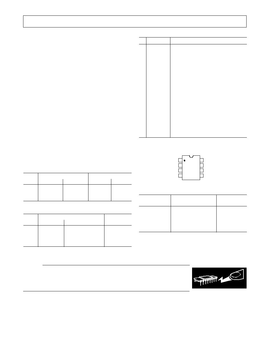
PIN FUNCTION DESCRIPTION
Pin Mnemonic
Function
1
RO
Receiver Output. When enabled if A > B
by 200 mV, then RO = High. If A < B by
200 mV, then RO = Low.
2
RE
Receiver Output Enable. A low level enables
the receiver output, RO. A high level places
it in a high impedance state.
3
DE
Driver Output Enable. A high level enables
the driver differential outputs, A and B. A
low level places it in a high impedance state.
4
DI
Driver Input. When the driver is enabled a
logic Low on DI forces A low and B high
while a logic High on DI forces A high and
B low.
5
GND
Ground Connection, 0 V.
6
A
Noninverting Receiver Input A/Driver
Output A.
7
B
Inverting Receiver Input B/Driver Output B.
8
V
CC
Power Supply, 5 V
± 5%.
PIN CONFIGURATION
TOP VIEW
(Not to Scale)
8
7
6
5
1
2
3
4
RO
RE
DE
V
CC
B
A
GND
DI
ADM1485
ORDERING GUIDE
Temperature
Package
Model
Range
Option
ADM1485JN
0
°C to +70°C
N-8
ADM1485JR
0
°C to +70°C
SO-8
ADM1485AN
40
°C to +85°C
N-8
ADM1485AR
40
°C to +85°C
SO-8
ADM1485AQ
40
°C to +85°C
Q-8
CAUTION
ESD (electrostatic discharge) sensitive device. Electrostatic charges as high as 4000 V readily
accumulate on the human body and test equipment and can discharge without detection. Although
the ADM1485 features proprietary ESD protection circuitry, permanent damage may occur on
devices subjected to high-energy electrostatic discharges. Therefore, proper ESD precautions are
recommended to avoid performance degradation or loss of functionality.
WARNING!
ESD SENSITIVE DEVICE
ADM1485
REV. A
4
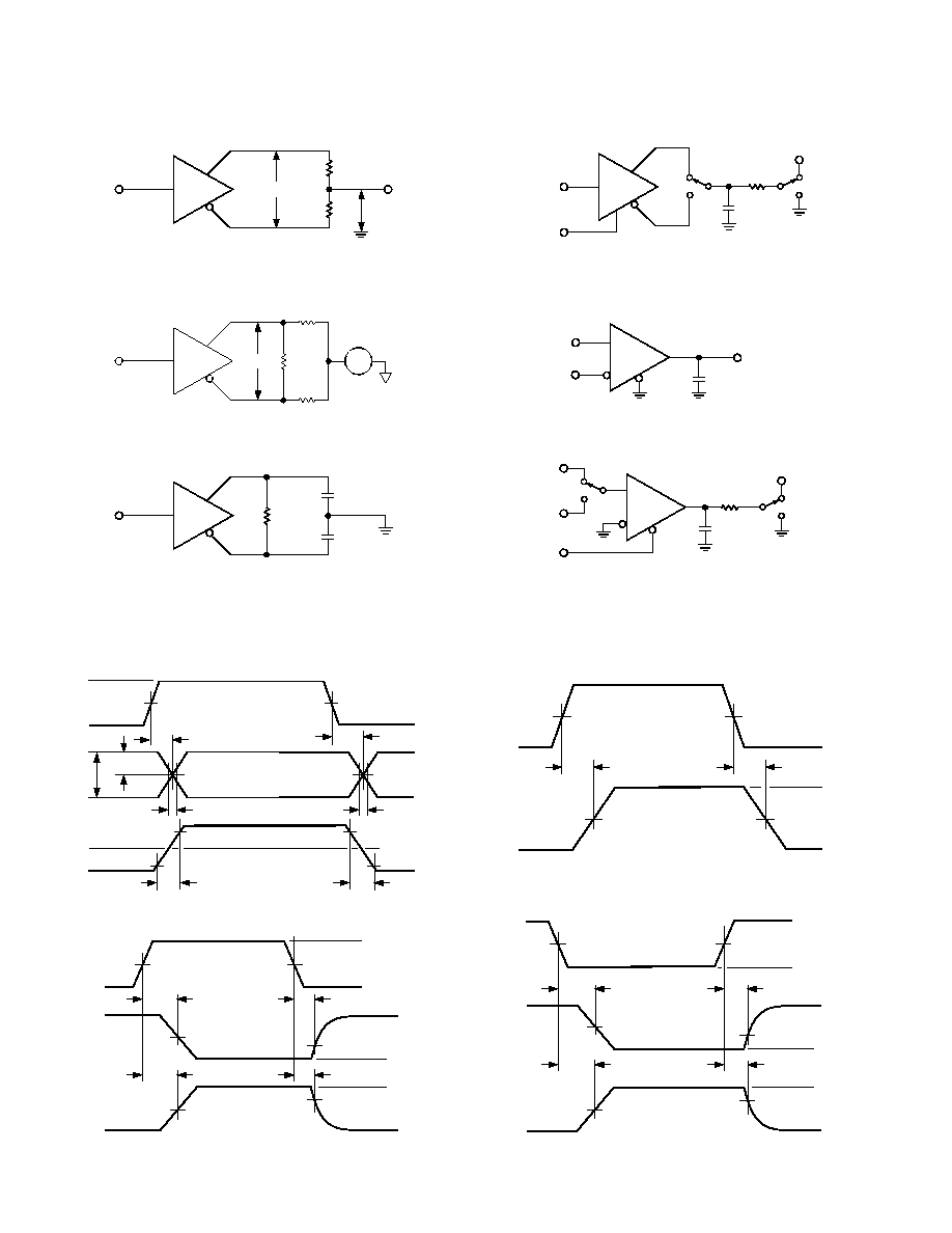
Test Circuits
V
OD
R
R
V
OC
Figure 1. Driver Voltage Measurement Test Circuit
V
OD3
60
375
375
V
TST
Figure 2. Driver Voltage Measurement Test Circuit 2
R
LDIFF
A
B
C
L1
C
L2
Figure 3. Driver Propagation Delay Test Circuit
DE
0V OR 3V
DE IN
A
B
S1
C
L
V
OUT
R
L
S2
V
CC
Figure 4. Driver Enable/Disable Test Circuit
RE
A
B
C
L
V
OUT
Figure 5. Receiver Propagation Delay Test Circuit
RE
+1.5V
RE IN
S1
C
L
V
OUT
R
L
S2
V
CC
1.5V
Figure 6. Receiver Enable/Disable Test Circuit
Switching Characteristics
3V
0V
B
A
0V
VO
VO
90% POINT
10% POINT
T
R
T
SKEW
1/2VO
T
PLH
1.5V
1.5V
T
PHL
T
SKEW
90% POINT
10% POINT
T
F
VO
Figure 7. Driver Propagation Delay, Rise/Fall Timing
DE
A, B
A, B
1.5V
2.3V
2.3V
T
ZH
T
ZL
1.5V
3V
0V
V
OL
V
OH
0V
V
OL
+0.5V
V
OH
0.5V
T
HZ
T
LZ
Figure 8. Driver Enable/Disable Timing
A, B
RO
0V
T
PLH
1.5V
0V
T
PHL
1.5V
V
OH
V
OL
Figure 9. Receiver Propagation Delay
RE
R
R
1.5V
1.5V
1.5V
T
ZH
T
ZL
1.5V
3V
0V
V
OL
V
OH
V
OL
+0.5V
V
OH
0.5V
T
HZ
T
LZ
O/P LOW
O/P HIGH
0V
Figure 10. Receiver Enable/Disable Timing
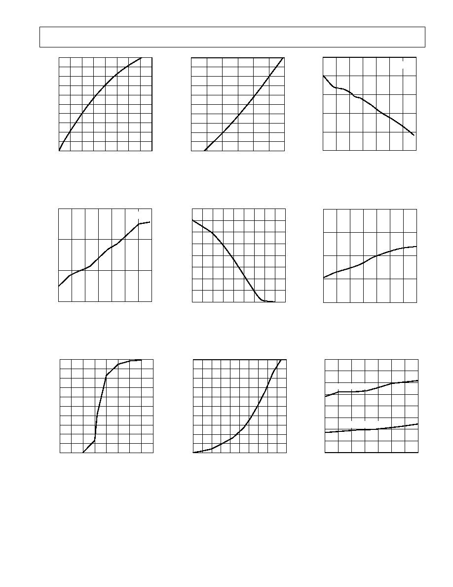
Typical Performance CharacteristicsADM1485
REV. A
5
OUTPUT VOLTAGE Volts
OUTPUT CURRENT
mA
40
0
36
32
28
24
20
16
12
8
4
0
0.5
1.0
1.5
2.0
Figure 11. Receiver Output Low
Voltage vs. Output Current
TEMPERATURE C
OUTPUT VOLTAGE
Volts
0.4
0.3
0.1
50
0.2
25
0
25
50
75
100
125
I = 8mA
Figure 14. Receiver Output Low
Voltage vs. Temperature
OUTPUT VOLTAGE Volts
OUTPUT CURRENT
mA
100
0
0
4
1
2
3
90
60
50
30
10
80
70
40
20
Figure 17. Driver Output Low
Voltage vs. Output Current
OUTPUT VOLTAGE Volts
OUTPUT CURRENT
mA
0
3.5
2
4
6
8
10
12
14
16
18
20
4.0
4.5
5.0
Figure 12. Receiver Output High
Voltage vs. Output Current
OUTPUT VOLTAGE Volts
OUTPUT CURRENT
mA
96
0
84
72
60
48
36
24
12
0
1
2
3
4
Figure 15. Driver Differential Out-
put Voltage vs. Output Current
OUTPUT VOLTAGE Volts
OUTPUT CURRENT
mA
0
0
10
20
30
40
50
60
70
80
90
100
1
2
3
4
5
Figure 18. Driver Output High
Voltage vs. Output Current
TEMPERATURE C
OUTPUT VOLTAGE
Volts
5.0
4.9
4.5
50
25
125
0
25
50
75
100
4.8
4.7
4.6
I = 8mA
Figure 13. Receiver Output High
Voltage vs. Temperature
TEMPERATURE C
DIFFERENTIAL VOLTAGE
Volts
2.4
2.3
2.0
50
25
125
0
25
50
75
100
2.2
2.1
Figure 16. Driver Differential Output
Voltage vs. Temperature, R
L
= 54
TEMPERATURE C
50
SUPPLY CURRENT
mA
1.00
25
0
25
50
75
100
125
0.95
0.90
0.85
0.80
0.75
0.70
0.65
0.60
DRIVER ENABLED
DRIVER DISABLED
Figure 19. Supply Current vs.
Temperature
ADM1485Typical Performance Characteristics
REV. A
6
TEMPERATURE C
TIME
ns
5
4
0
50
3
2
1
25
0
25
50
75
100
125
Figure 20. Receiver t
PLH
t
PHL
vs.
Temperature
10
0%
100
90
5ns
500mV
500mV
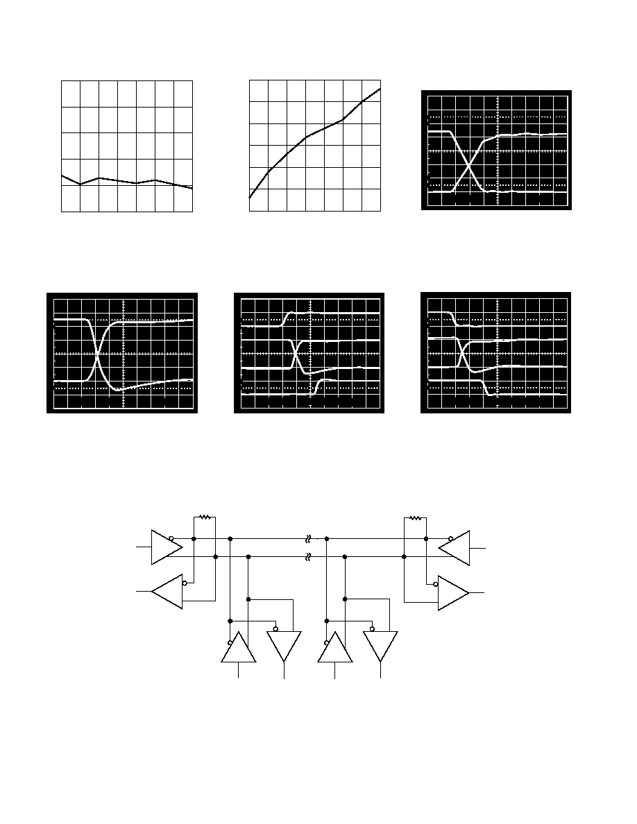
Figure 23. Loaded Driver
Differential Outputs
RT
RT
D
R
D
D
R
R
D
R
Figure 26. Typical RS-485 Network
TEMPERATURE C
TIME
ns
1.0
50
0.9
0.8
0.7
0.6
0.5
0.4
25
0
25
50
75
100
125
Figure 21. Driver Skew vs.
Temperature
10
0%
100
90
H
O
1V
1V
5
5
10ns
Figure 24. Driver/Receiver Propaga-
tion Delays Low to High
10
0%
100
90
5ns
1V
1V
Figure 22. Unloaded Driver
Differential Outputs
10
0%
100
90
H
O
1V
1V
5
5
10ns
Figure 25. Driver/Receiver Propaga-
tion Delays High to Low
ADM1485
REV. A
7
APPLICATIONS INFORMATION
Differential Data Transmission
Differential data transmission is used to reliably transmit data at
high rates over long distances and through noisy environments.
Differential transmission nullifies the effects of ground shifts and
noise signals which appear as common-mode voltages on the
line. There are two main standards approved by the Electronics
Industries Association (EIA) which specify the electrical charac-
teristics of transceivers used in differential data transmission.
The RS-422 standard specifies data rates up to 10 MBaud and
line lengths up to 4000 ft. A single driver can drive a transmis-
sion line with up to 10 receivers.
In order to cater for true multipoint communications, the
RS-485 standard was defined. This standard meets or exceeds
all the requirements of RS-422 but also allows for up to 32
drivers and 32 receivers to be connected to a single bus. An
extended common-mode range of 7 V to +12 V is defined. The
most significant difference between RS-422 and RS-485 is the
fact that the drivers may be disabled thereby allowing more than
one (32 in fact) to be connected to a single line. Only one driver
should be enabled at time, but the RS-485 standard contains
additional specifications to guarantee device safety in the event
of line contention.
Cable and Data Rate
The transmission line of choice for RS-485 communications is a
twisted pair. Twisted pair cable tends to cancel common-mode
noise and also causes cancellation of the magnetic fields gener-
ated by the current flowing through each wire, thereby, reducing
the effective inductance of the pair.
The ADM1485 is designed for bidirectional data communica-
tions on multipoint transmission lines. A typical application
showing a multipoint transmission network is illustrated in
Figure 26. An RS-485 transmission line can have as many as 32
transceivers on the bus. Only one driver can transmit at a par-
ticular time but multiple receivers may be enabled simultaneously.
As with any transmission line, it is important that reflections are
minimized. This may be achieved by terminating the extreme
ends of the line using resistors equal to the characteristic im-
pedance of the line. Stub lengths of the main line should also be
kept as short as possible. A properly terminated transmission
line appears purely resistive to the driver.
Thermal Shutdown
The ADM1485 contains thermal shutdown circuitry which
protects the part from excessive power dissipation during fault
conditions. Shorting the driver outputs to a low impedance
source can result in high driver currents. The thermal sensing
circuitry detects the increase in die temperature and disables the
driver outputs. The thermal sensing circuitry is designed to
disable the driver outputs when a die temperature of 150
°C is
reached. As the device cools, the drivers are re-enabled at
140
°C.
Propagation Delay
The ADM1485 features very low propagation delay ensuring
maximum baud rate operation. The driver is well balanced
ensuring distortion free transmission.
Another important specification is a measure of the skew be-
tween the complementary outputs. Excessive skew impairs the
noise immunity of the system and increases the amount of elec-
tromagnetic interference (EMI).
Receiver Open-Circuit Fail Safe
The receiver input includes a fail-safe feature which guarantees
a logic high on the receiver when the inputs are open circuit or
floating.
Table III. Comparison of RS-422 and RS-485 Interface Standards
Specification
RS-422
RS-485
Transmission Type
Differential
Differential
Maximum Cable Length
4000 ft.
4000 ft.
Minimum Driver Output Voltage
±2 V
±1.5 V
Driver Load Impedance
100
54
Receiver Input Resistance
4 k
min
12 k
min
Receiver Input Sensitivity
±200 mV
±200 mV
Receiver Input Voltage Range
7 V to +7 V
7 V to +12 V
No of Drivers/Receivers Per Line
1/10
32/32
ADM1485
REV. A
8
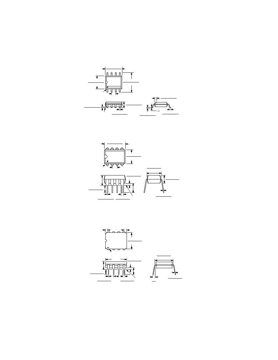
OUTLINE DIMENSIONS
Dimensions shown in inches and (mm).
8-Lead SOIC (SO-8)
0.0098 (0.25)
0.0075 (0.19)
0.0500 (1.27)
0.0160 (0.41)
8
0
0.0196 (0.50)
0.0099 (0.25)
45
8
5
4
1
0.1968 (5.00)
0.1890 (4.80)
0.2440 (6.20)
0.2284 (5.80)
PIN 1
0.1574 (4.00)
0.1497 (3.80)
0.0500 (1.27)
BSC
0.0688 (1.75)
0.0532 (1.35)
SEATING
PLANE
0.0098 (0.25)
0.0040 (0.10)
0.0192 (0.49)
0.0138 (0.35)
8-Lead Plastic DIP (N-8)
SEATING
PLANE
0.060 (1.52)
0.015 (0.38)
0.210
(5.33)
MAX
0.022 (0.558)
0.014 (0.356)
0.160 (4.06)
0.115 (2.93)
0.070 (1.77)
0.045 (1.15)
0.130
(3.30)
MIN
8
1
4
5
PIN 1
0.280 (7.11)
0.240 (6.10)
0.100 (2.54)
BSC
0.430 (10.92)
0.348 (8.84)
0.195 (4.95)
0.115 (2.93)
0.015 (0.381)
0.008 (0.204)
0.325 (8.25)
0.300 (7.62)
8-Lead Cerdip (Q-8)
8
1
4
5
0.310 (7.87)
0.220 (5.59)
PIN 1
0.005 (0.13)
MIN
0.055 (1.4)
MAX
SEATING
PLANE
0.023 (0.58)
0.014 (0.36)
0.200 (5.08)
MAX
0.150
(3.81)
MIN
0.070 (1.78)
0.030 (0.76)
0.200 (5.08)
0.125 (3.18)
0.100
(2.54)
BSC
0.060 (1.52)
0.015 (0.38)
0.405 (10.29)
MAX
15
°
0
°
0.320 (8.13)
0.290 (7.37)
0.015 (0.38)
0.008 (0.20)
C181806/00 (rev. A) 00063
PRINTED IN U.S.A.