 | ÐлекÑÑоннÑй компоненÑ: ADM1487JN | СкаÑаÑÑ:  PDF PDF  ZIP ZIP |
Äîêóìåíòàöèÿ è îïèñàíèÿ www.docs.chipfind.ru
PRELIMINARY TECHNICAL DATA
GENERAL DESCRIPTION
The ADM1487 is an ultra-low power RS-485/RS-422
transceiver consisting of one driver and one receiver per
package. Quiescent operating current is typically 80µA
and 1µA in shutdown mode. The driver and receiver both
have three-state outputs. This allows multiple drivers to be
connected to an RS-485/RS-422 bus, or several receiver
outputs to be connected to a serial data bus. The driver
will maintain a high-impedance output state even with
power off, while the receiver features fail-safe operation
that guarantees a logic high output if the inputs are left
open-circuit.
The device has slew-rate limited drivers to minimize elec-
tromagnetic interference (EMI) and reduce reflections
caused by incorrectly terminated cables.
FEATURES
Low Power - 120µA Max ICC with Driver Disabled
High Input Impedance -- Up to 256 Transceivers on Bus
Low-Current (1µA) Shutdown Mode
Slew Rate Control for Error-Free Data
Transmission and Low EMI
±10kV ESD Protection (Human Body Model) on
RS-485 I/O pins
Thermal Protection of Driver
Glitch-Free Driver Power-Up Allows Hot Connection
Driver Maintains High Output Impedance with Power
Off
Wide Common-Mode Range Allows ±7V Ground Differ-
ences Between Devices
Pin-Compatible with Industry Standard 75176
APPLICATIONS
Battery-Powered RS-485/RS-422 Systems
Level Translation
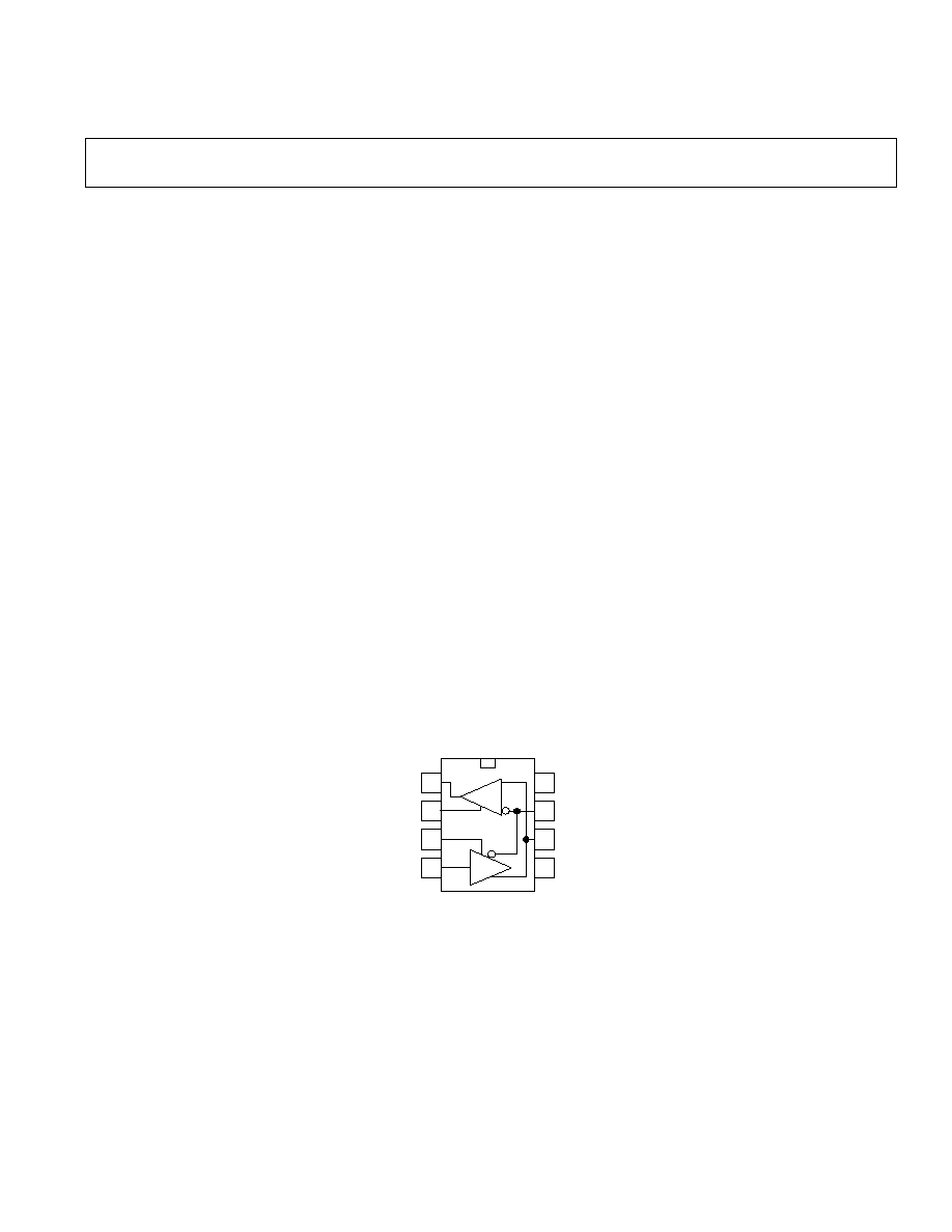
FUNCTIONAL BLOCK DIAGRAM
1
2
3
4
8
7
6
5
D
R
RO
RE
DE
DI
V
CC
B
A
GND
ADM1487
1
ADM1487
a
REV. PrC 08/02
Information furnished by Analog Devices is believed to be accurate and
reliable. However, no responsibility is assumed by Analog Devices for its
use, nor for any infringements of patents or other rights of third parties
which may result from its use. No license is granted by implication or
otherwise under any patent or patent rights of Analog Devices.
One Technology Way, P.O. Box 9106, Norwood, MA 02062-9106, U.S.A.
Tel: 781/329-4700
www.analog.com
Fax: 781/326-8703
Analog Devices, Inc., 2002
Preliminary Technical Data
Ultra-Low Power RS-485/RS-422 Transceiver
with Low EMI and +/-10kV ESD Protection

ADM1487
2
Rev. PrC
PRELIMINARY TECHNICAL DATA
ADM1487 SPECIFICATIONS
DC ELECTRICAL CHARACTERISTICS
(V
CC
= +5V ±5%, T
A
= 0°C TO +70°C, UNLESS OTHERWISE NOTED)
Parameter
Min
Typ
Max
Units
Test Conditions/Comments
Differential Driver Output Voltage,V
OD1
5
V
Unloaded, I
O
= 0
Differential Driver Output Voltage, V
OD2
2.0
V
Figure 1, R = 50 (RS-422)
1.5
5
V
Figure 1, R = 27
(RS-485)
Change in Magnitude of Driver
0.2
V
Figure 1, R = 27 or R = 50
Differential Output Voltage for
Complementary Output States,
VOD
Driver Common-Mode Output
3
V
Figure 1, R = 27 or R = 50
Voltage, V
OC
Change in Magnitude of Driver
0.2
V
R = 27 or R = 50
Common-Mode Output Voltage for
Complementary Output States, |V
OC
|
Input High Voltage (DE, DI,
RE), V
IH
2
V
Input Low Voltage (DE, DI,
RE), V
IL
0.8
V
Input Current (DE, DI,
RE), I
IN1
± 2
µ A
Input Current (A, B), I
IN2
0.30
m A
DE = 0, V
CC
= 0V or 5.25V, V
IN
= 12V
-0.15
m A
DE = 0, V
CC
= 0V or 5.25V, V
IN
= 7V
Differential Input Threshold Voltage
-0.2
0.2
V
7V
V
CM
12V
for Receiver, V
TH
Receiver Input Hysteresis, V
TH
45
m V
V
CM
= 0V
Receiver Output High Voltage, V
OH
3.5
V
I
O
=-4mA, V
ID
= 200mV
Receiver Output Low Voltage, V
OL
0.4
V
I
O
= 4mA, V
ID
= 200mV
Three-State (High Impedance) Output
± 1
µ A
V
CC
= Max, 0.4V Vo 2.4V
Current at Receive, I
OZR
Receiver Input Resistance, R
IN
70
96
k
7V
V
CM
12V
Supply Current, I
CC
120
200
µ A
No Load, Output Enabled
80
120
µ A
No Load, Output Disabled
Supply Current in Shutdown Mode, I
SHDN
1
10
µ A
DE = 0V,
RE = V
CC
Driver Short-Circuit Ourrent, I
OSD1
35
250
m A
V
OUT
= HIGH, 7V V
O
12V
Driver Short-Circuit Ourrent, I
OSD2
35
250
m A
V
OUT
= LOW, 7V Vo 12V
Receiver Short-Circuit Current, I
OSR
7
85
m A
0V
V
O
V
OC

ADM1487
Rev. PrC
3
ADM1487 SPECIFICATIONS (continued)
ELECTRICAL CHARACTERISTICS
(VCC = +5V ±5%, TA = -40°C TO +85°C, UNLESS OTHERWISE NOTED)
Parameter
Min
Typ
Max
Units Test Conditions/Comments
Differential Driver Output Voltage, V
OD1
5
V
Unloaded, I
O
= 0
Differential Driver Output Voltage, V
OD2
2.0
V
Figure 1, R = 50 (RS-422)
1.5
5
V
Figure 1, R = 27 (RS-485)
Driver Common-Mode
3
V
Figure 1, R = 27 or R = 50
Output Voltage, V
OC
Differential Input Threshold
0.2
0.2
V
7V
V
CM
12V
Voltage for Receiver, V
TH
Receiver Input Hysteresis, V
TH
45
m V
V
CM
= 0V
Supply Current, I
CC
120
200
µ A
No Load, Output Enabled
80
120
µ A
No Load, Output Disabled
Supply Current in Shutdown Mode, I
SHDN
1
10
µ A
DE = 0V,
RE = V
CC
Driver Input to Output High, t
DPLH
150
1200
ns
Figures 2, 3, R
DIFF
= 54 ,
C
L1
= C
L2
= 100pF
Driver Input to Output Low, t
DPHL
150
1200
ns
Figures 2, 3, R
DIFF
= 54 ,
C
L1
= C
L2
= 100pF
Driver Output to Output, t
SKEW
100
600
ns
Figures 2, 3, R
DIFF
= 54 ,
C
L1
= C
L2
= 100pF
Driver Rise or Fall Time, t
DR
, t
DF
150
2000
ns
Figures 2, 3, R
DIFF
= 54 ,
C
L1
= C
L2
= 100pF
Receiver Input to Output High, t
RPLH
30
140
250
ns
Figures 2, 4, R
DIFF
= 54 ,
C
L1
= C
L2
= 100pF
Receiver Input to Output Low, t
RHL
30
140
250
ns
Figures 2, 4, R
DIFF
= 54 ,
C
L1
= C
L2
= 100pF
Differential Receiver Skew, t
SKD
13
ns
Figures 2, 4, R
DIFF
= 54 ,
|t
RPLH
-t
RPHL
|
C
L1
= C
L2
= 100pF
Maximum Data Rate, f
MAX
250
kbps
SWITCHING CHARACTERISTICS
(V
CC
= +5V ±5%, T
A
= -40°C TO +85°C, UNLESS OTHERWISE NOTED)
Parameter
Min
Typ
Max
Units
Test Conditions/Comments
Driver Input to Output High, t
DPLH
150
1200
ns
Figures 2, 3, R
DIFF
= 54 ,
C
L1
= C
L2
= 100pF
Driver Input to Output, t
DPHL
150
1200
ns
Figures 2, 3, R
DIFF
= 54 ,
C
L1
= C
L2
= 100pF
Driver Output to Output, t
SKEW
250
600
ns
Figures 2, 3, R
DIFF
= 54 ,
C
L1
= C
L2
= 100pF
Driver Rise or Fall Time, t
DR
, t
DF
150
1200
ns
Figures 2, 3, R
DIFF
= 54 ,
C
L1
= C
L2
= 100pF
Driver Enable to Output High, t
DZH
100
1500
ns
Figures 5, 6, C
L
= 100pF, S2 Closed
Driver Enable to Output Low, t
DZL
100
1500
ns
Figures 5, 6, C
L
= 100pF, S1 Closed
Driver Disable Time from Low, t
DLZ
150
1500
ns
Figures 5, 6, C
L
= l5pF, S1 Closed
PRELIMINARY TECHNICAL DATA
ADM1487
4
Rev. PrC
PRELIMINARY TECHNICAL DATA
ADM1487 SPECIFICATIONS (continued)
SWITCHING CHARACTERISTICS
(V
CC
= +5V ±5%, T
A
= -40°C TO +85°C, UNLESS OTHERWISE NOTED)
Parameter
Min
Typ
Max
Units Test Conditions/Comments
Driver Disable Time from High, t
DHZ
150
1500
ns
Figures 5, 6, C
L
= l5pF, S2 Closed
Receiver Input to Output, t
RPLH
30
140
250
ns
Figures.2, 4, R
DIFF
= 54 ,
C
L1
= C
L2
= 100pF
Receiver Input to Output Low, t
RPHL
30
140
250
ns
Figures.2, 4, R
DIFF
= 54 ,
C
L1
= C
L2
= 100pF
DifferentialReceiverSkew, t
SKD
13
ns
Figures.2, 4, R
DIFF
= 54 ,
|t
PLH
-t
PHL
|
C
L1
= C
L2
= 100pF
Receiver Enable to Output Low, t
RZL
20
50
ns
Figures 7, 8, C
RL
= l5pF, S1 Closed
Receiver Enable to Output High, t
RZH
20
50
ns
Figures 7, 8, C
RL
= l5pF, S2 Closed
Receiver Disable from Low, t
RLZ
20
50
ns
Figures 7, 8, C
RL
= l5pF, S1 Closed
Receiver Disable from High, t
RHZ
20
50
ns
Figures 7, 8, C
RL
= l5pF, S2 Closed
Maximum Data Rate, f
MAX
250
kbps
Time to Shutdown, t
SHDN
50
200
600
ns
DE = 0,
RE = low to high transition
Driver Enable from Shutdown to
2000
ns
Figures 5, 6, C
L
= 100pF, S2 Closed
Output High, t
DZH(SHDN)
Driver Enable from Shutdown to
2000
ns
Figures 5, 6, C
L
= 100pF, S1 Closed
Output Low, t
DZL(SHDN)
Receiver Enable from Shutdown to
2000
ns
Figures 7, 8, C
L
= l5pF, S2 Closed
Output High, t
RZH(SHDN)
Receiver Enable from Shutdown to
2000
ns
Figures 7, 8, C
L
= l5pF, S1 Closed
Output Low, t
RZL(SHDN)
NOTES
1
Absolute maximum ratings are those beyond which the safety of the device cannot be guaranfeed.
2
All currents into device pins are positive; all currents out ot device pins are negative. All voltages are referenced to device ground unless otherwise specified.
3
All typicals are given for Vcc = 5V and Tp = 25°C.
4
The ADM1487 is not tested and is not quality-assurance sampled at -40°C and at 85°C. These specifications are guaranteed by design, correlation, andlor inference from
0°C, 25°C and/or 70°C tests.
ABSOLUTE MAXIMUM RATINGS
Supply Voltage (Vcc) . . . . . . . . . . . . . . . . . . . . . . . . . . 12V
Control Input Voltage . . . . . . . . . . . 0.5V to Vcc + 0.5V
Driver Input Voltage . . . . . . . . . . . 0.5V to Vcc + 0.5V
Driver Output Voltage . . . . . . . . . . . . . . . . . . . . . . . . ±14V
Receiver InputVoltage . . . . . . . . . . . . . . . . . . . . . . . . ±14V
Receiver Output Voltage . . . . . . . . . 0.5V to Vcc + 0.5V
Operating Temperature Range . . . . . . 0°C
T
A
70°C
Lead Temperature (Soldering, 10 sec) . . . . . . . . . 300°C
*Stresses above those listed under "Absolute Maximum Ratings" may cause permanent
damage to the device. This is a stress rating only; functional operation of the device
at these or any other conditions above those indicated in the operational section of this
specification is not implied. Exposure to absolute maximum rating conditions for
extended periods may affect device reliability.
THERMAL CHARACTERISTICS
8-Pin Plastic DIP Package
JA
= tbd K/Watt,
JC
= tbd K/Watt
8-Pin Plastic SO Package
JA
= tbd K/Watt,
JC
= tbd K/Watt
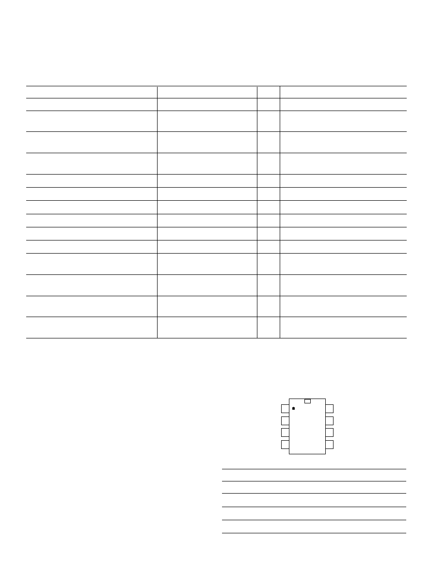
PIN CONFIGURATION
ORDERING INFORMATION
Model
Temperature Range
Package Option
ADM1487JN
0°C to +70°C
8 Pin Plastic DIP
ADM1487JR
0°C to +70°C
8 Pin SO
ADM1487AN
40°C to +85°C
8 Pin Plastic DIP
ADM1487AR
40°C to +85°C
8 Pin SO
ADM1487
TOP VIEW
(Not to Scale)
RO
RE
DE
DI
V
CC
B
A
GND
1
2
3
4
8
7
6
5
ADM1487
Rev. PrC
5
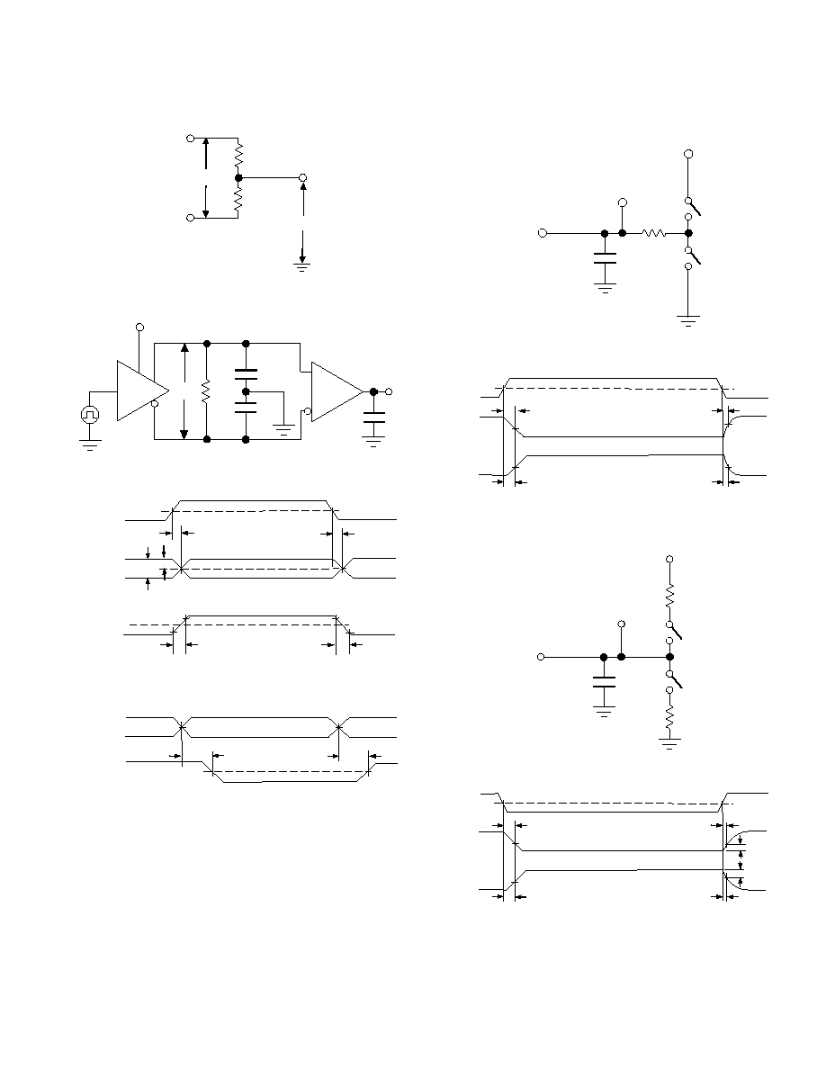
R
R
V
OD
V
OC
A
A
Figure 1. Driver DC Load Test Circuit
R
DIFF
V
OD2
C
L1
C
L2
3V
DE
DI
RO
D
R
15pF
A
B
A
B
Figure 2. Driver/Receiver Timing Test Circuit
DI
B
A
V
0
/2
V
0
t
DF
V
DIFF
V
0
-V
0
0V
90%
10%
t
DR
90%
10%
t
SKEW
= |t
DPLH
-t
DPHL
|
3V
0V
1.5V
t
DPLH
t
DPHL
V
DIFF
= V
A
- V
B
f = 1MHz, t
r
#
10ns, t
f
#
10ns
Figure 3. Driver Propagation Delays
RO
A
B
V
OD2
-V
OD2
V
OH
V
OL
1.5V
t
RPLH
t
RPHL
f = 1MHz, t
r
#
10ns, t
f
#
10ns
Figure 4. Receiver Propagation Delays
ADM1487 TEST CIRCUITS AND TIMING
V
CC
S1
S2
TEST
POINT
C
RL
15pF
500
V
OUTPUT
UNDER
TEST
Figure 5. Test Load for Driver Enable/Disable Time Test
3V
0V
DE
A, B
A, B
V
OL
t
DZL(SHDN)
, t
DZL
t
DLZ
OUTPUT NORMALLY LOW
OUTPUT NORMALLY HIGH
1.5V
2.3V
V
OL
+ 0.5V
V
OH
- 0.5V
V
OL
t
DZH(SHDN)
,
t
DZH
t
DHZ
2.3
V
f = 1MHz, t
r
#
10ns, t
f
#
10ns
5V
V
OH
Figure 6. Driver Enable and Disable Times
RO
TEST
POINT
V
CC
1k
V
1k
V
S1
S2
C
RL
15pF
Figure 7. Test Load for Receiver Enable/Disable Time Test
OUTPUT NORMALLY LOW
OUTPUT NORMALLY HIGH
3V
0V
RE
RO
RO
t
RZL(SHDN)
, t
RZL
t
RLZ
1.5
V
0.5V
0.5V
0V
t
RZH(SHDN)
, t
RZH
t
RHZ
1.5
V
5V
1.5
V
5V
f = 1MHz, t
r
#
10ns, t
f
#
10ns
Figure 8. Receiver Enable and Disable Delay Times
PRELIMINARY TECHNICAL DATA
ADM1487
6
Rev. PrC
PRELIMINARY TECHNICAL DATA
ADM1487 TYPICAL PERFORMANCE CHARACTERISTICS
A W
A
IT
IN
G
D
A T
A
TPC1. No-load Supply Current vs. Tem-
perature
AW
A I
TI
NG
D
A
TA
TPC2. Output Current vs. Receiver Out-
put High Voltage
A W
A I
TI
N G
D
A
TA
TPC3. Output Current vs. Receiver Out-
put Low Voltage
A W
A I
TI
N G
D
A
TA
TPC4. Receiver Output High
Voltage vs. Temperature
A W
A I
TI
N G
D
A
TA
TPC5. Receiver Output Low
Voltage vs. Temperature
A W
A I
TI
N G
D
A
TA
TPC6. Shutdown Current vs.
Temperature
PIN FUNCTION DESCRIPTION
Pin
Mnemonic
Description
1
R O
Receiver Output. When
RE is low and A - B
(more positive than) 200mV, RO will be high.
When
RE is low and A - B (more negative than) 200mV, RO will be low.
2
R E
Receiver Output Enable. Take
RE low to enable RO; RO is high impedance when RE is high.
Take
RE high and DE low to enter low-power shutdown mode.
3
D E
Driver Output Enable. Take DE high to enable driver outputs. These outputs are high
impedance when DE is low. Take RE high and DE low to enter low-power shutdown mode.
4
D I
Driver Input. With DE high, a low on DI forces non-inverting output low and inverting output
high. Similarly, a high on DI forces non-inverting output high and inverting output low.
5
G N D
Ground
6
A
Non-Inverting Receiver Input and Non-Inverting Driver Output
7
B
Inverting Receiver Input and Inverting Driver Output
8
V
CC
Positive Supply 4.75V =V
CC
=5.25V
ADM1487
Rev. PrC
7
TRANSMITTING
INPUTS
OUTPUTS
R E
D E
DI
Z
Y
X
1
1
0
1
X
1
0
1
0
0
0
X
H i g h - Z
H i g h - Z
1
0
X
Shutdown*
X = Don't care
CIRCUIT DESCRIPTION
The ADM1487 is a differential input, differential output
transceiver designed RS-485/RS-422 serial data communi-
cations over twisted-pair cables. It is a half-duplex device
intended for alternate transmission and reception of data
over a single twisted-pair cable, and the driver outputs and
receiver inputs are internally linked and brought out to a
single pair of pins.
Its principal features include ultra-low power operation, a
controlled slew-rate driver that minimizes electromagnetic
interference (EMI) and signals reflections due to incor-
rectly terminated lines, and high input impedance that al-
lows up to 256 receivers to be connected to a bus.
THREE-STATE BUS CONNECTION
The ADM1487 has a Driver Enable pin (DE) that enables
the driver outputs when taken high or puts the driver out-
puts into a high-impedance state when taken low. This al-
lows several driver outputs to be connected to an RS-422/
RS-485 bus.
Similarly, the device has a (active-low) Receiver Enable
pin (
RE). Taking this low enables the receiver, while tak-
ing it high puts the receiver outputs into a high-impedance
state. This allows several receiver outputs to be connected
to a serial data bus.
The input impedance of the device is 96k , which is 8
times higher than the standard RS-485 load of 12k . A
standard driver can driver 32 standard loads, so up to 256
ADM1487 receivers, or a combination of ADM1487 and
other devices up to 32 unit loads, may be connected to an
RS-422/RS485 bus driven by a single driver.
LOW POWER OPERATION
The ADM1487 draws very little supply current (typically
80µA) when the driver outputs are disabled or unloaded.
This will increase by up to 72µA if the driver outputs are
enabled (but unloaded) and applying the maximum output
swing of 5V across the receiver input resistors.
However, in practical applications with the device driving
and RS-485/RS422 cable or bus, the current drain is
dominated by the current sourced into the line termination
resistors and any other devices on the bus. With a half-ter-
mination (120 load) between the driver outputs, the load
current can be in excess of 13mA as the drivers force a
minimum of 1.5V across the line, and can be greater than
25mA with a fully terminated 60 line attached.
DEVICE TRUTH TABLES
SHUTDOWN MODE
If
RE is taken high while DE is taken low, the device will
enter a low-power shutdown mode, in which the supply
current is typically 1µA.
If the driver outputs are active immediately before shut-
down (DE high), the supply current will not drop to 1µ
until the driver outputs have settled to their three-state
mode, which can take up to 2.6µs worst-case. If DE is al-
ready low and shutdown is entered by taking
RE high, the
supply current will drop to 1µA very quickly.
When
RE is taken low and/or DE is takem high, the de-
vice will wake up within 3.5µs.
If shutdown mode is not used, the fact that DE is active-
high and
RE is active-low offers a convenient way of
switching the device between transmit and receive, by ty-
ing DE and
RE together. This is useful, for example, in
applications using half duplex operation and where several
receiver outputs are connected to a serial bus.
The device is guaranteed not to enter shutdown mode if
DE and
RE are driven in this way. If DE is low and RE is
high for less than 50ns the device will not enter shutdown.
If DE is low and
RE is high for greater than 600ns, the
device is guaranteed to enter shutdown.
RECEIVER INPUTS
The ADM1487 receiver has an input common-mode
range covering the entire RS-485 range of 7V to 12V.
Internal 96k
input resistors from each line terminal to
ground provide a 1/8 unit load to the RS485 bus.
Differential signals greater than ±200mV within the speci-
fied input common-mode range are converted to a TTL-
compatible logic signal at the receiver output. A small
amount of input hysteresis is included to minimize the ef-
fects of noise on the line signals. If the line is terminated
or the receiver inputs are shorted together, the receiver
output will retain the last valid line signal due to the
45mV of hysteresis incorporated in the receiver circuit. If
the receiver inputs are left floating (unterminated), an in-
ternal pull-up of 10µA at the A input will force the re-
ceiver output to a guranteed high output state.
DRIVER OUTPUT STAGE
The RS-485 specification requires that a transceiver with-
stand common-mode voltages of up to 12V above or 7V
below system ground at the RS-485 line connections.
In addition, the transceiver must be protected against both
ESD and latch-up. This precludes the use of conventional
RECEIVING
INPUTS
OUTPUT
R E
D E
A-B
R O
0
X
0.2V
1
0
X
-0.2V
0
0
X
Open/shorted
1
1
0
X
Shutdown*
*In shutdown mode, driver and receiver outputs high impedance
PRELIMINARY TECHNICAL DATA
ADM1487
8
Rev. PrC
PRELIMINARY TECHNICAL DATA
CMOS outout stages, which include parasitic diodes from
their driver outputs to each supply rail and can latch up
when these diodes conduct.
V
C C
P A RA S ITIC
DIO DE D
P
P A RA S IT IC
D IO D E D
P
S CH O T T KY
RE V E RS E -BIA S E D
W H E N O UT P UT
> V
C C
+V
D
S C HO TT K Y
R E V E R S E -B IAS E D
W HE N O U TP U T
< G N D - V
D
Figure 9. ADM1487 Driver Output Stage
The ADM1487 output includes Schottky diodes in series
with the positive supply to the drain of the P-channel output
device and in series with the drain of the N-channel output
device. These diodes prevent the P-channel's parasitic diode
from conducting when the output voltage exceeds V
CC
and
prevent the N-channel's parasitic diode from conducting
when the output voltage falls below ground.
SLEW RATE CONTROL
The driver output stage of the ADM1487 has a controlled
slew rate to minmize signal reflections on incorrectly termi-
nated lines and to reduce electromagnetic interference (EMI).
CURRENT LIMIT AND THERMAL SHUTDOWN
The ADM1487 incorporates two protection mechanisms to
guard the drivers against short-circuits, bus contention or
other fault conditions. The first is a current-limited output
stage that protects the driver against short-circuits over the
entire common-mode voltage range by limiting the output
current to about 70mA. Under extreme fault condtions
where the current limit is not effective, a thermal shutdown
circuit puts the driver outputs into a high-impedance state if
the die temperature exceeds 150°C, and does not turn them
back on until the temperature has fallen to 130°C.
ENHANCED ESD PROTECTION
All Analog Devices parts incorporate protection against
electrostatic discharge (ESD) to protect the devices dur-
ing handling, assembly and normal operation. In addition,
the ADM1487 has enhanced ESD protection up to ±10kV
on the A and B I/O pins to protect against severe opera-
tional conditions such as line transients, connection and
disconnection.
APPLICATION INFORMATION
Figure 10 shows a typical application of the ADM1487.
This is a half-duplex RS-485/RS-422 network. Up to 254
additional ADM1487s can be connected along the cable
(termination resistors are only required at each end).
Figure 10. Typical Half-Duplex RS-485/RS-422 Network
OUTLINE DIMENSIONS
Dimensions shown in inches and (mm).
8-Pin Plastic Dual-In-Line Package (N-8)
8
1 4
5
0. 43 0 (10 . 92 )
0. 34 8 (8.84 )
0. 28 0 (7.11 )
0. 24 0 (6.10 )
P IN 1
S E A TI N G
P L A N E
0. 02 2 (0.5 58 )
0. 01 4 (0.3 56 )
0. 06 0 (1. 52 )
0. 01 5 (0. 38 )
0.21 0 ( 5. 33 )
M A X
0.1 3 0
(3 .30 )
M IN
0.07 0 ( 1. 77 )
0.04 5 ( 1. 15 )
0.1 0 0
(2 .54 )
B S C
0. 16 0 (4.06 )
0. 11 5 (2.93 )
0. 32 5 (8. 25 )
0. 30 0 (7. 62 )
0. 01 5 (0. 3 81 )
0. 00 8 (0. 2 04 )
0. 19 5 (4. 95 )
0. 11 5 (2. 93 )
8-Pin SO Package (R-8)
8 5
4
1
0. 19 6 8 (5 . 00 )
0. 18 9 0 (4 . 80 )
0. 15 7 4 (4 . 00 )
0. 14 9 7 (3 . 80 )
0. 24 4 0 (6 . 20 )
0. 22 8 4 (5 . 80 )
P I N 1
S E A TI N G
P L A N E
0. 00 9 8 (0 .25 )
0. 00 4 0 (0 .10 )
0. 01 9 2 (0 . 49 )
0. 01 3 8 (0 . 35 )
0. 10 2 (2.59 )
0. 09 4 (2.39 )
0. 0 5 00
(1 . 27 )
B S C
0. 00 9 8 (0 .25 )
0. 00 7 5 (0 .19 )
0. 05 0 0 (1 .27 )
0. 01 6 0 (0 .41 )
8
0
0. 01 9 6 (0 .50 )
0. 00 9 9 (0 .25 )
x 4 5
100n
DI
D
R
5
6
7
8
4
3
2
1
ADM1487
DE
RO
100n
+5V
(V
CC
)
+5V (V
CC
)
R
T
R
T
DATA
IN (DI)
RECEIVER
OUTPUT
(RO)
1
2
3
4
8
7
6
5
D
R
RECEIVER
ENABLE
(
RE)
DRIVER
ENABLE
(DE)
ADM1487
CABLE TERMINATED
AT ENDS
ADDITIONAL
ADM1487s
A
B
A
B
A
B
RE