 | ÐлекÑÑоннÑй компоненÑ: ADM202JN | СкаÑаÑÑ:  PDF PDF  ZIP ZIP |
Äîêóìåíòàöèÿ è îïèñàíèÿ www.docs.chipfind.ru
FUNCTIONAL BLOCK DIAGRAMS
0.1µF
6.3V
0.1µF
6.3V
0.1µF
16V
0.1µF
6.3V
+5V TO +10V
VOLTAGE
DOUBLER
+10V TO 10V
VOLTAGE
INVERTER
0.1µF
16V
+5V INPUT
V
CC
V+
V
C1+
C1
C2+
C2
ADM202
6
GND
15
4
5
3
1
2
T1
IN
RS-232
OUTPUTS
TTL/CMOS
INPUTS
*
T1
OUT
T2
IN
R1
OUT
R2
OUT
T2
OUT
R1
IN
R2
IN
R1
R2
T2
T1
TTL/CMOS
OUTPUTS
RS-232
INPUTS
**
13
10
7
11
8
14
9
12
16
*
INTERNAL 400k PULL-UP RESISTOR ON EACH TTL/CMOS INPUT
**INTERNAL 5k PULL-DOWN RESISTOR ON EACH RS-232 INPUT
+5V INPUT
V
CC
V+
V
C1+
C1
C2+
C2
GND
ADM203
7
T1
IN
RS-232
OUTPUTS
TTL/CMOS
INPUTS
*
T1
OUT
T2
IN
R1
OUT
R2
OUT
T2
OUT
R1
IN
R2
IN
R1
R2
T2
T1
TTL/CMOS
OUTPUTS
RS-232
INPUTS
**
4
1
18
2
19
5
20
3
8
13
12
17
14
11
15
10
16
V
C2
C2+
9
6
GND
DO NOT MAKE
CONNECTIONS TO
THESE PINS
INTERNAL
10V POWER
SUPPLY
INTERNAL
+10V POWER
SUPPLY
REV. 0
Information furnished by Analog Devices is believed to be accurate and
reliable. However, no responsibility is assumed by Analog Devices for its
use, nor for any infringements of patents or other rights of third parties
which may result from its use. No license is granted by implication or
otherwise under any patent or patent rights of Analog Devices.
a
High Speed, +5 V, 0.1 F
CMOS RS-232 Driver/Receivers
ADM202/ADM203
One Technology Way, P.O. Box 9106, Norwood, MA 02062-9106, U.S.A.
Tel: 617/329-4700
Fax: 617/326-8703
GENERAL DESCRIPTION
The ADM202/ADM203 is a two-channel RS-232 line driver/
receiver pair designed to operate from a single +5 V power sup-
ply. A highly efficient on-chip charge pump design permits
RS-232 levels to be developed using charge pump capacitors as
small as 0.1
µ
F. The capacitors are internal to the package on
the ADM203 so no external capacitors are required. These con-
verters generate
±
10 V RS-232 output levels.
The ADM202/ADM203 meets or exceeds the EIA-232-E and
V.28 specifications. Fast driver slew rates permit operation up to
120 kB while high drive currents allows for extended cable
lengths.
An epitaxial BiCMOS construction minimizes power consump-
tion to 10 mW and also guards against latch-up. Overvoltage
protection is provided allowing the receiver inputs to withstand
continuous voltages in excess of
±
30 V. In addition, all pins
contain ESD protection to levels greater than 2 kV.
The ADM202 is available in 16-lead DIP and both narrow and
wide SOIC packages. The ADM203 is available in a 20-pin DIP
package.
FEATURES
120 kB Transmission Rate
ADM202: Small (0.1 F) Charge Pump Capacitors
ADM203: No External Capacitors Required
Single 5 V Power Supply
Meets EIA-232-E and V.28 Specifications
Two Drivers and Two Receivers
On-Board DC-DC Converters
9 V Output Swing with +5 V Supply
Low Power BiCMOS: 2.0 mA I
CC
30 V Receiver Input Levels
APPLICATIONS
Computers
Peripherals
Modems
Printers
Instruments
ADM202/ADM203SPECIFICATIONS
REV. 0
2
(V
CC
= +5 V 10%, (ADM202 C1C4 = 0.1 F. All Specifications
T
MIN
to T
MAX
, unless otherwise noted)
Parameter
Min
Typ
Max
Units
Conditions/Comments
Output Voltage Swing
±
5
±
9
V
V
CC
= 5 V
±
5%, T1
OUT
, T2
OUT
Loaded with
3 k
to GND
Output Voltage Swing
±
5
±
9
V
V
CC
= 5 V
±
10%, T
A
= +25
°
C, T1
OUT
, T2
OUT
Loaded with 3 k
to GND
V
CC
Power Supply Current.
1.5
2
mA
No Load, T1
IN
, T2
lN
= V
CC
3.0
4
mA
No Load, T1
IN
, T2
IN
= GND
Input Logic Threshold Low, V
INL
0.8
V
T
IN
Input Logic Threshold High, V
INH
2.0
V
T
IN
Logic Pull-Up Current
10
25
µ
A
T
IN
= 0 V
RS-232 Input Voltage Range
30
+30
V
RS-232 Input Threshold Low
0.8
1.2
V
RS-232 Input Threshold High
1.7
2.4
V
RS-232 Input Hysteresis
0.2
0.5
1.0
V
RS-232 Input Resistance
3
5
7
k
TTL/CMOS Output Voltage Low, V
OL
0.4
V
I
OUT
= 1.6 mA
TTL/CMOS Output Voltage High, V
OH
3.5
V
I
OUT
= 1.0 mA
Propagation Delay
0.5
5
µ
s
RS-232 to TTL
Instantaneous Slew Rate
1
25
30
V/
µ
s
C
L
= 10 pF, R
L
= 37 k
, T
A
= +25
°
C
Transition Region Slew Rate
5
V/
µ
s
R
L
= 3 k
, C
L
= 2500 pF
Measured from +3 V to 3 V or 3 V to +3 V
Baud Rate
120
kB
R
L
= 3 k
, C
L
= 1 nF
Output Resistance
300
V
CC
= V+ = V = 0 V, V
OUT
=
±
2 V
RS-232 Output Short Circuit Current
±
10
±
60
mA
NOTE
1
Sample tested to ensure compliance.
Specifications subject to change without notice.
ABSOLUTE MAXIMUM RATINGS*
(T
A
= +25
°
C unless otherwise noted)
V
CC
. . . . . . . . . . . . . . . . . . . . . . . . . . . . . . . . . . . . . . . . . .+6 V
V+ . . . . . . . . . . . . . . . . . . . . . . . . . . . (VCC 0.3 V) to +14 V
V . . . . . . . . . . . . . . . . . . . . . . . . . . . . . . . . . . +0.3 V to 14 V
Input Voltages
T
IN
. . . . . . . . . . . . . . . . . . . . . . . . . . 0.3 V to (V
CC
+ 0.3 V)
R
IN
. . . . . . . . . . . . . . . . . . . . . . . . . . . . . . . . . . . . . . . .
±
30 V
Output Voltages
T
OUT
. . . . . . . . . . . . . . . . . . . (V+, +0.3 V) to (V, 0.3 V)
R
OUT
. . . . . . . . . . . . . . . . . . . . . . . . 0.3 V to (V
CC
+ 0.3 V)
Short Circuit Duration
T
OUT
. . . . . . . . . . . . . . . . . . . . . . . . . . . . . . . . . Continuous
Power Dissipation
N-16 DIP . . . . . . . . . . . . . . . . . . . . . . . . . . . . . . . . . 470 mW
R-16N SOIC . . . . . . . . . . . . . . . . . . . . . . . . . . . . . . 600 mW
R-16W SOIC . . . . . . . . . . . . . . . . . . . . . . . . . . . . . . 500 mW
N-20 DIP . . . . . . . . . . . . . . . . . . . . . . . . . . . . . . . . . 890 mW
Thermal Impedance
N-16 DIP . . . . . . . . . . . . . . . . . . . . . . . . . . . . . . . . 135
°
C/W
R-16N SOIC . . . . . . . . . . . . . . . . . . . . . . . . . . . . . 105
°
C/W
R-16W SOIC . . . . . . . . . . . . . . . . . . . . . . . . . . . . . 105
°
C/W
N-20 DIP . . . . . . . . . . . . . . . . . . . . . . . . . . . . . . . . 125
°
C/W
Operating Temperature Range
Commercial (J Version) . . . . . . . . . . . . . . . . . . 0
°
C to +70
°
C
Storage Temperature Range . . . . . . . . . . . . . 65
°
C to +150
°
C
Lead Temperature Soldering
Vapor Phase (60 sec) . . . . . . . . . . . . . . . . . . . . . . . . +215
°
C
Infrared (15 sec) . . . . . . . . . . . . . . . . . . . . . . . . . . . . +220
°
C
ESD Rating . . . . . . . . . . . . . . . . . . . . . . . . . . . . . . . . . >2000 V
*This is a stress rating only and functional operation of the device at these or any
other conditions above those indicated in the operation sections of this specifica-
tion is not implied. Exposure to absolute maximum rating conditions for extended
periods of time may affect reliability.
ORDERING GUIDE
Model
Temperature Range
Package Option
ADM202JN
0
°
C to +70
°
C
N-16
ADM202JRN
0
°
C to +70
°
C
R-16N
ADM202JRW
0
°
C to +70
°
C
R-16W
ADM203JN
0
°
C to +70
°
C
N-20
ADM202/ADM203
REV. 0
3
PIN CONFIGURATIONS
DIP/SOIC
1
2
3
4
5
6
7
8
16
15
14
13
12
11
10
9
Top View
(Not to Scale)
ADM202
T1
IN
R1
IN
T1
OUT
R1
OUT
V+
V
CC
GND
T2
IN
R2
IN
T2
OUT
R2
OUT
V
C1+
C1
C2
C2+
DIP
1
2
3
4
5
6
7
8
9
10
20
19
18
17
16
15
14
13
12
11
Top View
(Not to Scale)
ADM203
R1
IN
T2
IN
R2
IN
T1
OUT
T2
OUT
R1
OUT
V+
V
V
CC
C1+
C2
C2+
C1
GND
GND
C2+
C2
R2
OUT
V
T1
IN
0.1µF
6.3V
0.1µF
6.3V
0.1µF
16V
0.1µF
6.3V
+5V TO +10V
VOLTAGE
DOUBLER
+10V TO 10V
VOLTAGE
INVERTER
0.1µF
16V
+5V INPUT
V
CC
V+
V
C1+
C1
C2+
C2
ADM202
6
GND
15
4
5
3
1
2
T1
IN
RS-232
OUTPUTS
TTL/CMOS
INPUTS
*
T1
OUT
T2
IN
R1
OUT
R2
OUT
T2
OUT
R1
IN
R2
IN
R1
R2
T2
T1
TTL/CMOS
OUTPUTS
RS-232
INPUTS
**
13
10
7
11
8
14
9
12
16
*
INTERNAL 400k PULL-UP RESISTOR ON EACH TTL/CMOS INPUT
**INTERNAL 5k PULL-DOWN RESISTOR ON EACH RS-232 INPUT
+5V INPUT
V
CC
V+
V
C1+
C1
C2+
C2
GND
ADM203
7
T1
IN
RS-232
OUTPUTS
TTL/CMOS
INPUTS
*
T1
OUT
T2
IN
R1
OUT
R2
OUT
T2
OUT
R1
IN
R2
IN
R1
R2
T2
T1
TTL/CMOS
OUTPUTS
RS-232
INPUTS
**
4
1
18
2
19
5
20
3
8
13
12
17
14
11
15
10
16
V
C2
C2+
9
6
GND
DO NOT MAKE
CONNECTIONS TO
THESE PINS
INTERNAL
10V POWER
SUPPLY
INTERNAL
+10V POWER
SUPPLY
Figure 1. Typical Operating Circuits
PIN FUNCTION DESCRIPTION
Mnemonic
Function
V
CC
Power Supply Input 5 V
±
10%.
V+
Internally Generated Positive Supply (+10 V nominal).
V
Internally Generated Negative Supply (10 V nominal).
GND
Ground Pin. Must be connected to 0 V.
C1+
ADM202 External Capacitor, (+ terminal) is connected to this pin.
ADM203: The capacitor is connected internally and no external capacitor is required.
C1
ADM202 External Capacitor, ( terminal) is connected to this pin.
ADM203: The capacitor is connected internally and no external capacitor is required.
C2+
ADM202 External Capacitor, (+ terminal) is connected to this pin.
ADM203: The capacitor is connected internally and no external capacitor is required.
C2
ADM202 External Capacitor, ( terminal) is connected to this pin.
ADM203: The capacitor is connected internally and no external capacitor is required.
T
IN
Transmitter (Driver) Inputs. These inputs accept TTL/CMOS levels. An internal 400 k
pull-up resistor to V
CC
is
connected on each input.
T
OUT
Transmitter (Driver) Outputs. These are RS-232 levels (typically
±
10 V).
ADM202/ADM203
REV. 0
4
R
IN
Receiver Inputs. These inputs accept RS-232 signal levels. An internal 5 k
pull-down resistor to GND is
connected on each of these inputs.
R
OUT
Receiver Outputs. These are TTL/CMOS levels.
GENERAL INFORMATION
The ADM202/ADM203 is an RS-232 drivers/receivers designed
to solve interface problems by meeting the EIA-232E specifica-
tions while using a single digital +5 V supply. The EIA standard
requires transmitters that will deliver
±
5 V minimum on the
transmission channel and receivers that can accept signal levels
down to
±
3 V. The parts achieve this by integrating step up
voltage converters and level shifting transmitters and receivers
onto the same chip. CMOS technology is used to keep the
power dissipation to an absolute minimum.
The ADM203 uses internal capacitors and, therefore, no exter-
nal capacitors are required.
The ADM202 contains an internal voltage doubler and a voltage
inverter which generates
±
10 V from the +5 V input. External
0.1
µ
F capacitors are required for the internal voltage converter.
The ADM202/ADM203 is a modification, enhancement and
improvement to the AD230AD241 family and derivatives
thereof. It is essentially plug-in compatible and does not have
materially different applications.
CIRCUIT DESCRIPTION
The internal circuitry consists of three main sections. These are
(a) A Charge Pump Voltage Converter
(b) RS-232 to TTL/CMOS Receivers
(c) TTL/CMOS to RS-232 Transmitters
Charge Pump DC-DC Voltage Converter
The charge pump voltage converter consists of an oscillator and
a switching matrix. The converter generates a
±
10 V supply
from the input 5 V level. This is done in two stages using a
switched capacitor technique as illustrated below. First, the 5 V
input supply is doubled to 10 V using capacitor C1 as the
charge storage element. The 10 V level is then inverted to gen-
erate 10 V using C2 as the storage element.
Capacitors C3 and C4 are used to reduce the output ripple.
Their values are not critical and can be reduced if higher levels
of ripple are acceptable. The charge pump capacitors C1 and
C2 may also be reduced at the expense of higher output imped-
ance on the V+ and V supplies. On the ADM203, all capaci-
tors C1 to C4 are molded into the package.
The V+ and V supplies may also be used to power external
circuitry if the current requirements are small.
S1
S3
V+ = 2V
CC
S2
S4
INTERNAL
OSCILLATOR
C1
C3
V
CC
GND
V
CC
Figure 2. Charge Pump Voltage Doubler
S1
S3
S2
S4
INTERNAL
OSCILLATOR
C2
C4
V = (V+)
GND
V+
GND
FROM
VOLTAGE
DOUBLER
Figure 3. Charge Pump Voltage Inverter
Transmitter (Driver) Section
The drivers convert TTL/CMOS input levels into EIA-232-E
output levels. With V
CC
= +5 V and driving a typical EIA-232-E
load, the output voltage swing is
±
9 V. Even under worst case
conditions the drivers are guaranteed to meet the
±
5 V
EIA-232-E minimum requirement.
The input threshold levels are both TTL and CMOS compat-
ible with the switching threshold set at V
CC
/4. With a nominal
V
CC
= 5 V the switching threshold is 1.25 V typical. Unused
inputs may be left unconnected, as an internal 400 k
pull-up
resistor pulls them high forcing the outputs into a low state.
As required by the EIA-232-E standard the slew rate is limited
to less than 30 V/
µ
s without the need for an external slew limiting
capacitor and the output impedance in the power-off state is
greater than 300
.
Receiver Section
The receivers are inverting level shifters that accept EIA-232-E
input levels (
±
5 V to
±
15 V) and translate them into 5 V TTL/
CMOS levels. The inputs have internal 5 k
pull-down resistors
to ground and are also protected against overvoltages of up to
±
30 V. The guaranteed switching thresholds are 0.8 V minimum
and 2.4 V maximum which are well within the
±
3 V EIA-232
requirement. The low level threshold is deliberately positive as it
ensures that an unconnected input will be interpreted as a low
level.
The receivers have Schmitt trigger input with a hysteresis level
of 0.5 V. This ensures error free reception both for noisy inputs
and for inputs with slow transition times.
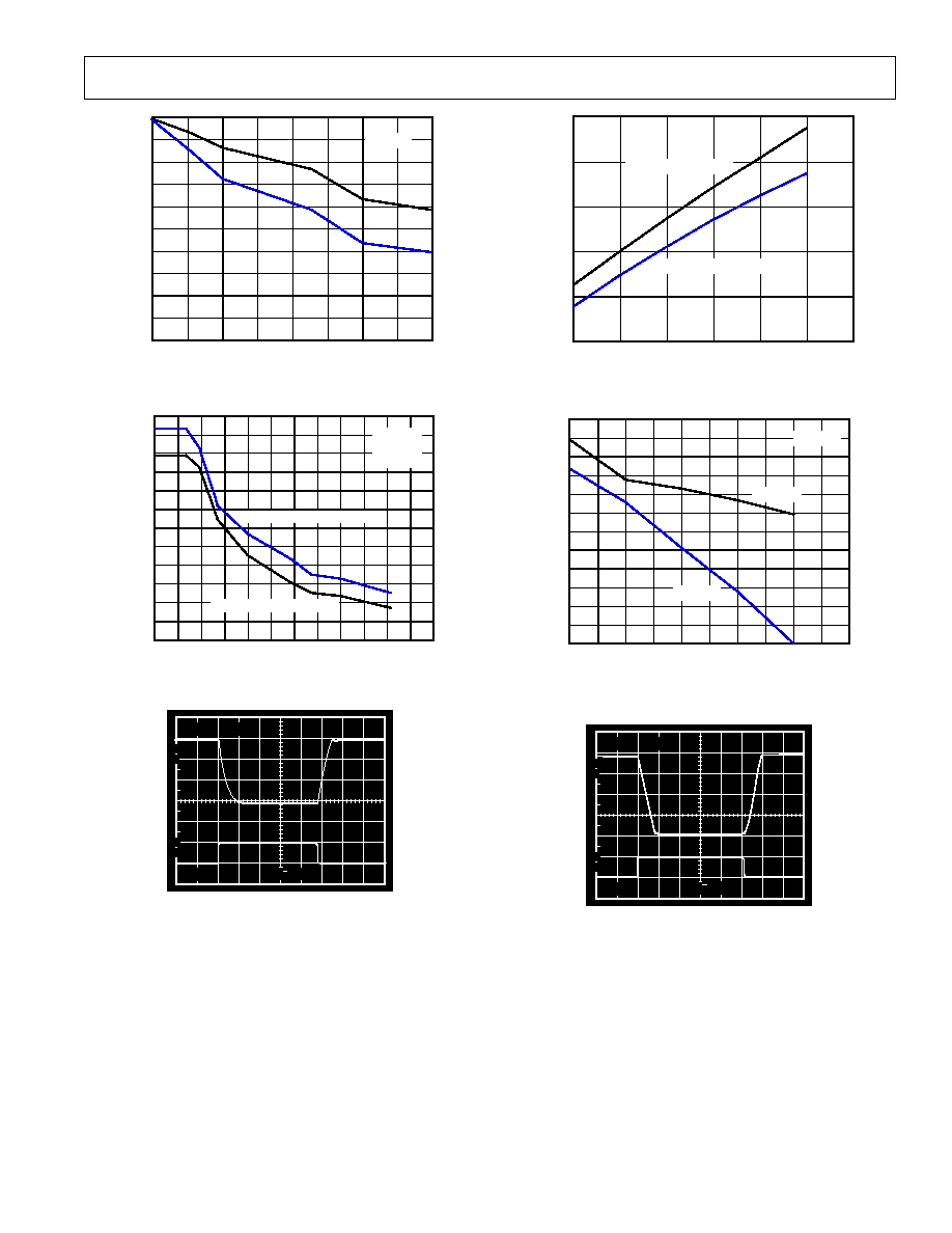
Typical Performance CharacteristicsADM202/ADM203
REV. 0
5
10
0
40
2
0
6
4
8
30
20
10
I
OUT
mA
V
CC
= 5V
V+
V
| V
OUT
| V
Figure 4. Charge Pump V+, V vs. Current
30
0
3k
5
0
15
10
20
25
2.5k
2k
1.5k
1k
500
V
CC
= 5V
R
L
= 3k
f = 10kHz
CAPACITIVE LOAD pF
SLEW RATE V/µs
LOW TO HIGH SLEW RATE
HIGH TO LOW SLEW RATE
Figure 5. Transmitter Slew Rate vs. Load Capacitance
10
90
100
0%
5V
3.6 V
A1
5v
5µs
Figure 6. Transmitter Fully Loaded Slew Rate
8
3
6
6
4
5
3
7
5
4
V
CC
V
| V
OUT
| V
V
OUT
(1 O/P LOADED)
V
OUT
(ALL O/Ps LOADED)
Figure 7. Transmitter Output Voltage vs. V
CC
12
0
10
2
0
6
4
8
10
8
6
4
2
V
CC
= 5V
I
OUT
mA
T
OUT
V
T
OUT
HIGH
T
OUT
LOW
Figure 8. Transmitter Output Voltage vs. Current
10
90
100
0%
5V
3.6 V
A1
5v
1µs
Figure 9. Transmitter Unloaded Slew Rate
ADM202/ADM203
REV. 0
6
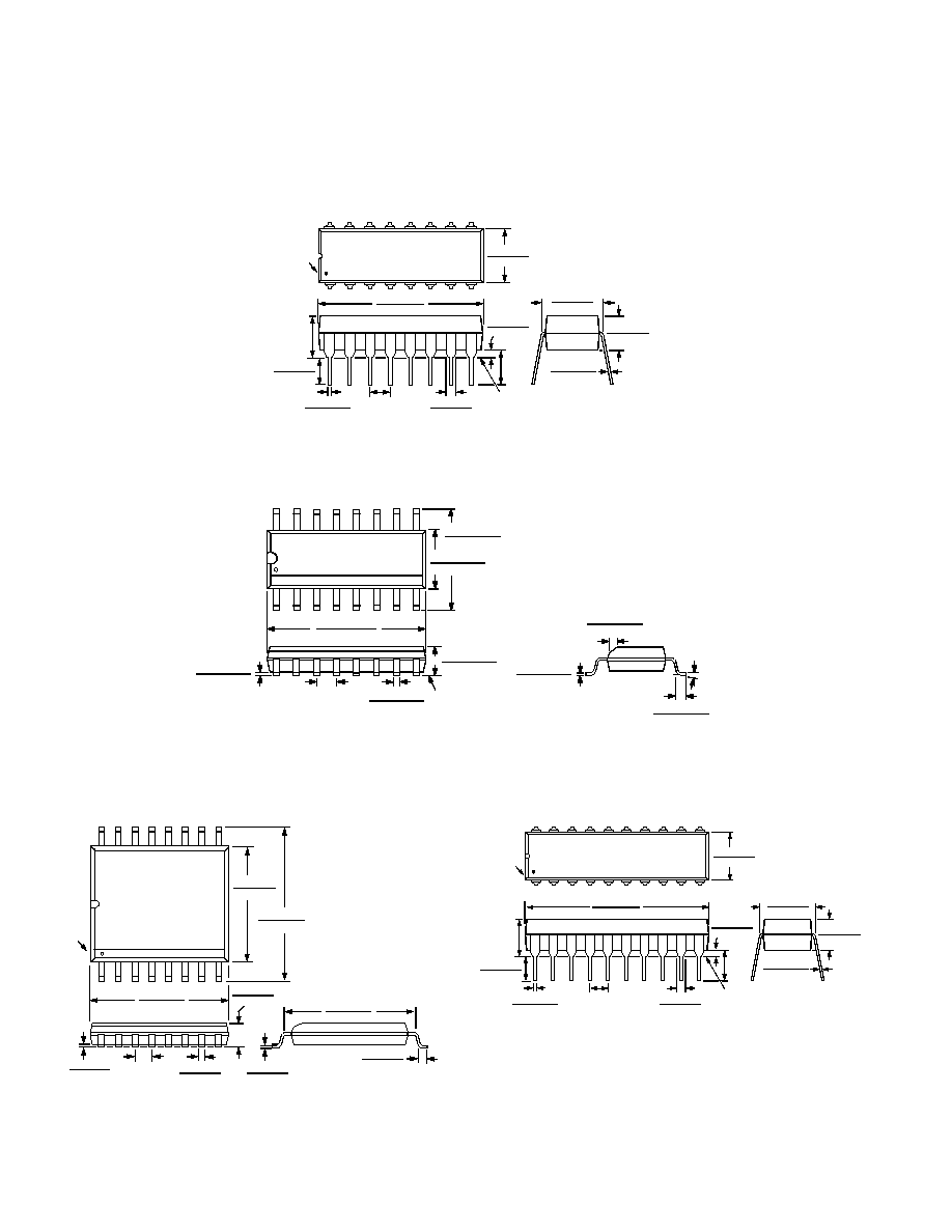
OUTLINE DIMENSIONS
Dimensions shown in inches and (mm).
C1899184/94
PRINTED IN U.S.A.
16-Pin Plastic DIP
(N-16)
0.325 (8.25)
0.300 (7.62)
0.015 (0.381)
0.008 (0.204)
0.195 (4.95)
0.115 (2.93)
PIN 1
0.280 (7.11)
0.240 (6.10)
9
16
1
8
0.840 (21.33)
0.745 (18.93)
0.210
(5.33)
0.200 (5.05)
0.125 (3.18)
0.022 (0.558)
0.014 (0.356)
0.100
(2.54)
BSC
SEATING
PLANE
0.060 (1.52)
0.015 (0.38)
0.150
(3.81)
0.070 (1.77)
0.045 (1.15)
16-Lead Narrow SOIC
(R-16N)
0.0500 (1.27)
BSC
SEATING
PLANE
8
9
16
1
0.0098 (0.25)
0.0040 (0.10)
0.0192 (0.49)
0.0138 (0.35)
0.0688 (1.75)
0.0532 (1.35)
0.3937 (10.00)
0.3859 (9.80)
0.2440 (6.20)
0.2284 (5.80)
0.1574 (4.00)
0.1497 (3.80)
×
45
°
0
°
8
°
0.0099 (0.25)
0.0075 (0.19)
0.0500 (1.27)
0.0160 (0.41)
0.0196 (0.50)
0.0099 (0.25)
20-Pin Plastic DIP
(N-20)
0.325 (8.25)
0.300 (7.62)
0.015 (0.381)
0.008 (0.204)
0.195 (4.95)
0.115 (2.93)
PIN 1
0.280 (7.11)
0.240 (6.10)
20
1
11
10
0.210
(5.33)
0.200 (5.05)
0.125 (3.18)
0.022 (0.558)
0.014 (0.356)
0.100
(2.54)
BSC
0.070 (1.78)
0.045 (1.15)
SEATING
PLANE
0.060 (1.52)
0.015 (0.38)
0.150
(3.81)
1.060 (26.90)
0.925 (23.50)
16-Lead Wide SOIC
(R-16W)
PIN 1
0.299 (7.60)
0.291 (7.40)
0.419 (10.65)
0.404 (10.26)
1
16
9
8
0.018 (0.46)
0.014 (0.36)
0.050 (1.27)
BSC
0.107 (2.72)
0.089 (2.26)
0.413 (10.50)
0.348 (10.10)
0.010 (0.25)
0.004 (0.10)
0.015 (0.38)
0.007 (1.18)
0.045 (1.15)
0.020 (0.50)
0.364 (9.246)
0.344 (8.738)