 | ÐлекÑÑоннÑй компоненÑ: ADM2209E | СкаÑаÑÑ:  PDF PDF  ZIP ZIP |
Äîêóìåíòàöèÿ è îïèñàíèÿ www.docs.chipfind.ru
REV. 0
Information furnished by Analog Devices is believed to be accurate and
reliable. However, no responsibility is assumed by Analog Devices for its
use, nor for any infringements of patents or other rights of third parties
which may result from its use. No license is granted by implication or
otherwise under any patent or patent rights of Analog Devices.
a
ADM2209E
One Technology Way, P.O. Box 9106, Norwood, MA 02062-9106, U.S.A.
Tel: 781/329-4700
World Wide Web Site: http://www.analog.com
Fax: 781/326-8703
© Analog Devices, Inc., 1999
EMI-/EMC-Compliant 15 kV ESD Protected,
Dual RS-232 Port with Standby
FEATURES
Two Complete Serial Ports, Six Drivers and Ten Receivers
Operates with 3 V or 5 V Logic
Low Power CMOS: <5 mA Operation
Low Standby Current: 100 A
460 kbit/s Data Rate Guaranteed Laplink
®
-Compatible
0.1 F Charge Pump Capacitors
Single +12 V Power Supply
+3.3 V/+5 V Standby Supply
One Receiver on Each Port Active in Standby
Complies with 89/336/EEC EMC Directive
ESD Protection to IEC1000-4-2 (801.2)
8 kV: Contact Discharge
15 kV: Air-Gap Discharge
15 kV: Human Body Model
Electrical Fast Transient (EFT) Immunity (IEC1000-4-4)
Low EMI Emissions (EN55022)
Eliminates Costly TransZorbs
®
Conforms to EIA/TIA-232-E Specifications
Fail-Safe Receiver Outputs
APPLICATIONS
Personal Computers
Printers
Peripherals
Modems
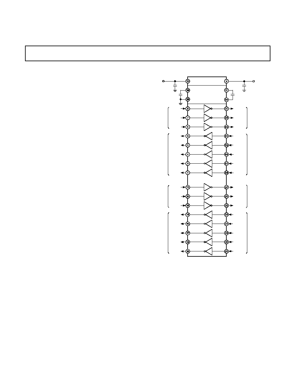
FUNCTIONAL BLOCK DIAGRAM
+
T1
R1
OUT
A
R1
IN
A
T2
R2
OUT
A
R2
IN
A
T3
T3
OUT
A
T3
IN
A
R1
T1
IN
A
T1
OUT
A
R5
R4
R3
R3
OUT
A
R4
OUT
A
R5
OUT
A
R3
IN
A
R4
IN
A
R5
IN
A
R2
T2
IN
A
T2
OUT
A
V
DD
T1
R1
OUT
B
R1
IN
B
T2
R2
OUT
B
R2
IN
B
T3
T3
OUT
B
T3
IN
B
R1
T1
IN
B
T1
OUT
B
R5
R4
R3
R3
OUT
B
R4
OUT
B
R5
OUT
B
R3
IN
B
R4
IN
B
R5
IN
B
R2
T2
IN
B
T2
OUT
B
GND
V
STBY
C+
C
0.1 F
0.1 F
CHARGE PUMP
VOLTAGE INVERTER
CMOS
INPUTS
CMOS
OUTPUTS
EIA/TIA-232
OUTPUTS
EIA/TIA-232
INPUTS
CMOS
INPUTS
CMOS
OUTPUTS
EIA/TIA-232
OUTPUTS
EIA/TIA-232
INPUTS
ADM2209E
0.1 F
0.1 F
3.3V/5V
+12V
+
GENERAL DESCRIPTION
The ADM2209E is a complete, dual RS-232 port on a single
chip, containing six drivers and ten receivers and fully meeting
EIA-232 and V.28 specifications. The device features an on-
board dc-to-dc converter to generate a 12 V power rail, elimi-
nating the need for a negative power supply.
The ADM2209E is suitable for operation in harsh electrical
environments and is compliant with the EU directive on EMC
(89/336/EEC). Both the level of emissions and immunity are in
compliance. EM immunity includes ESD protection in excess of
±
15 kV on all I-O lines (1000-4-2), Electrical Fast Transient
protection (1000-4-4) and Radiated Immunity (1000-4-3). EM
emissions include radiated and conducted emissions as required
by Information Technology Equipment EN55022, CISPR22.
The ADM2209E conforms to the EIA-232E and CCITT V.28
specifications and operates at data rates up to 460 kbps.
In standby mode, one receiver on each port (R5) remains active
to allow monitoring of peripheral devices while the rest of the
system is in power-saving mode. This feature allows the
ADM2209E to wake up the system when a peripheral device
begins communication.
The ADM2209E is available in a 38-lead TSSOP package.
Laplink is a registered trademark of Traveling Software, Inc.
TransZorb is a registered trademark of General Semiconductor Industries, Inc.

REV. 0
2
ADM2209ESPECIFICATIONS
(V
DD
= 10.8 V to 13.2 V, V
STBY
= 3.3 V 5% or 5 V 10%, C1 = C2 = 0.1 F. All
specifications T
MIN
to T
MAX
unless otherwise noted.)
Parameter
Min
Typ
1
Max
Units
Test Conditions/Comments
OPERATING CONDITIONS
Operating Voltage Range, V
DD
+10.8 +12 +13.2 V
Standby Voltage Range, V
STBY
+3.15
+5.5
V
V
DD
Power Supply Current
2
5
mA
No Load, All Driver Inputs at 0.8 V or 2 V,
All Receiver Inputs at +15 V or 15 V
V
STBY
Supply Current
100
200
µ
A
No Load, All Tx IN at V
STBY
or Open
TRANSMITTER (DRIVER) CMOS INPUTS
Input Pull-Up Current
10
25
µ
A
Transmitter Input at GND
High Level Input Voltage, V
INH
2.1
V
Low Level Input Voltage, V
INL
0.4
V
TRANSMITTER (DRIVER) EIA-232 OUTPUTS
Output Voltage Swing
±
5.0
±
9.0
V
All Transmitter Outputs Loaded with 3 k
to GND
Output Short-Circuit Current, I
OS
±
5
±
15
±
30
mA
V
O
= 0 V, V
IN
= 0.8 V
3
Output Resistance
300
V
DD
= 0 V, V
STBY
= 0 V, V
IN
=
±
2 V
RECEIVER EIA-232 INPUTS
Input Voltage Range
15
+15
V
Input Low Threshold, V
TL
0.4
1.45
V
Input High Threshold, V
TH
1.7
2.4
V
Input Hysteresis
0.25
V
Input Resistance, R
IN
3
5
7
k
V
IN
=
±
15 V
RECEIVER OUTPUTS
4
High Level Output Voltage, V
OH
2.4
V
I
OH
= 40
µ
A
Low Level Output Voltage, V
OL
0.2
0.4
V
I
OL
= +1.6 mA
Output Leakage Current (Except R5A, R5B)
0.05
±
5
µ
A
V
DD
= 0 V
DRIVER SWITCHING CHARACTERISTICS
5
Maximum Data Rate
460
kbps
R
L
= 3 k
to 7 k
, C
L
= 50 pF to 470 pF
460
kbps
R
L
= 3 k
to 7 k
, C
L
= 50 pF to 1000 pF,
T
A
= 0
°
C to +85
°
C, 5 V
±
10% Only
920
kbps
R
L
= 3 k
to 7 k
, C
L
= 50 pF to 470 pF,
V
STBY
= 5 V
±
5%, V
DD
= 12 V
±
5%
Propagation Delay, High to Low, T
PHL
1
µ
s
R
L
= 3 k
, C
L
= 1000 pF (Figures 1 and 2)
Propagation Delay, Low to High, T
PLH
1
µ
s
R
L
= 3 k
, C
L
= 1000 pF (Figures 1 and 2)
Transition Region Slew Rate
6
16
V/
µ
s
R
L
= 3 k
to 7 k
, C
L
= 50 pF to 470 pF
Transition Region Slew Rate (5 V)
4
16
V/
µ
s
R
L
= 3 k
to 7 k
, C
L
= 50 pF to 1000 pF,
V
STBY
= 5 V
±
10% Only. Measured from +3 V
to 3 V or Vice Versa
RECEIVER SWITCHING CHARACTERISTICS
Maximum Data Rate
920
kbps
C
L
= 150 pF, V
STBY
= 5 V
±
5% Only
460
kbps
C
L
= 150 pF
Propagation Delay, R1R4
0.4
0.75
µ
s
C
L
= 150 pF
Propagation Delay, R5
1
2
µ
s
C
L
= 150 pF
Output Rise Time, t
r
30
ns
Figures 3 and 4
Output Fall Time, t
f
30
ns
ESD AND EMC
ESD Protection (I-O Pins)
±
15
kV
Human Body Model
±
15
kV
IEC1000-4-2 Air Discharge
±
8
kV
IEC1000-4-2 Contact Discharge
ESD Protection
(All Other Pins)
±
2.5
kV
Human Body Model, MIL-STD-883B
EFT Protection (I-O Pins)
±
2
kV
IEC1000-4-4
EMI Immunity
10
V/m
IEC1000-4-3
NOTES
1
All typicals are given for V
DD
= +12 V, V
STBY
= 5 V, T
A
= +25
°
C.
2
Current into device pins is defined as positive. Current out-of-device pins is defined as negative. All voltages are referred to ground unless otherwise specified. For
current, minimum and maximum values are specified as an absolute value and the sign is used to indicate direction. For voltage logic levels, the more positive value is
designated as maximum. For example, if 6 V is a maximum, the typical value (6.8 V) is more negative.
3
Only one driver output shorted at a time.
4
If receiver inputs are unconnected, receiver output is a logic high.
5
Refer to typical curves. Driver output slew rate is measured from the +3.0 V to the 3.0 V level on the output waveform. Slew rate is determined by load capacitance.
Specifications subject to change without notice.
REV. 0
ADM2209E
3
ABSOLUTE MAXIMUM RATINGS*
(T
A
= +25
°
C unless otherwise noted)
V
STBY
. . . . . . . . . . . . . . . . . . . . . . . . . . . . . . . . 0.3 V to +7 V
V
DD
. . . . . . . . . . . . . . . . . . . . . . . . . . . . . . . . . . . . . . . . +14 V
Input Voltages
Driver Inputs Tn
IN
A/B . . . . . . . . . 0.3 V to (V
STBY
, +0.3 V)
Receiver Inputs Rn
IN
A/B . . . . . . . . . . . . . . . . . . . . . .
±
25 V
Output Voltages
Driver Outputs Tn
OUT
A/B . . . . . . . . . . . . . . . . . . . . .
±
15 V
Receiver Outputs Rn
OUT
A/B . . . . 0.3 V to (V
STBY
, +0.3 V)
Short Circuit Duration
Tn
OUT
A/B . . . . . . . . . . . . . . . . . . . . . . . . . . . . . Continuous
Power Dissipation
RU-38 TSSOP (Derate 12 mW/
°
C Above +70
°
C) . . . 1488 mW
Operating Temperature Range
Industrial (A Version) . . . . . . . . . . . . . . . . 40
°
C to +85
°
C
Storage Temperature Range . . . . . . . . . . . . 65
°
C to +150
°
C
Lead Temperature (Soldering, 10 sec) . . . . . . . . . . . . +300
°
C
ESD Rating (MIL-STD-883B) (I-O Pins) . . . . . . . . . .
±
15 kV
ESD Rating (MIL-STD-883B)
(Except I-O) . . . . . . . .
±
2.5 kV
ESD Rating
(IEC1000-4-2 Air) (I-O Pins) . . . . . . . . .
±
15 kV
ESD Rating
(IEC1000-4-2 Contact) (I-O Pins) . . . . . .
±
8 kV
EFT Rating (IEC1000-4-4) (I-O Pins) . . . . . . . . . . . . .
±
2 kV
*This is a stress rating only; functional operation of the device at these or any other
conditions above those indicated in the operation sections of this specification is
not implied. Exposure to absolute maximum rating conditions for extended
periods of time may affect reliability.
ORDERING GUIDE
Model
Temperature Range
Package Option
ADM2209EARU
40
°
C to +85
°
C
RU-38
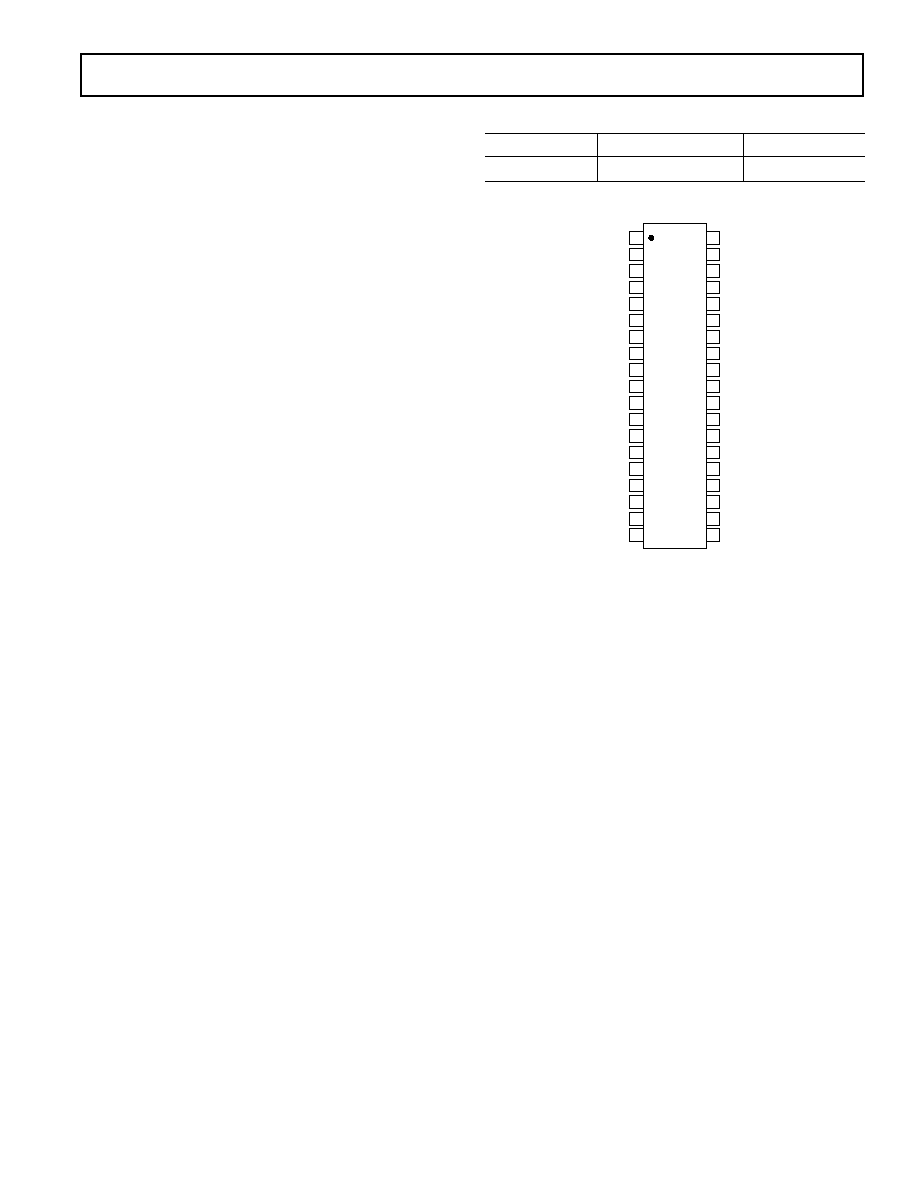
PIN CONFIGURATION
TOP VIEW
(Not to Scale)
38
37
36
35
34
33
32
31
30
29
28
27
26
25
24
23
22
21
20
1
2
3
4
5
6
7
8
9
10
11
12
13
14
15
16
17
18
19
ADM2209E
R5
IN
A
R4
IN
A
R3
IN
A
R2
IN
A
R1
IN
A
T3
OUT
A
T2
OUT
A
T1
OUT
A
V
C
GND
T1
OUT
B
T2
OUT
B
T3
OUT
B
R1
IN
B
R2
IN
B
R3
IN
B
R4
IN
B
R5
IN
B
R5
OUT
A
R4
OUT
A
R3
OUT
A
R2
OUT
A
R1
OUT
A
T3
IN
A
T2
IN
A
T1
IN
A
STBY
V
DD
C+
T1
IN
B
T2
IN
B
T3
IN
B
R1
OUT
B
R2
OUT
B
R3
OUT
B
R4
OUT
B
R5
OUT
B

REV. 0
ADM2209E
4
PIN FUNCTION DESCRIPTION
Pin Number
Mnemonic
Function
1
R5
OUT
A
Receiver Output (3.3 V/5 V TTL/CMOS Logic Levels)
2
R4
OUT
A
Receiver Output (3.3 V/5 V TTL/CMOS Logic Levels)
3
R3
OUT
A
Receiver Output (3.3 V/5 V TTL/CMOS Logic Levels)
4
R2
OUT
A
Receiver Output (3.3 V/5 V TTL/CMOS Logic Levels)
5
R1
OUT
A
Receiver Output (3.3 V/5 V TTL/CMOS Logic Levels)
6
T3
IN
A
Driver Input (3.3 V/5 V TTL/CMOS Logic Levels)
7
T2
IN
A
Driver Input (3.3 V/5 V TTL/CMOS Logic Levels)
8
T1
IN
A
Driver Input (3.3 V/5 V TTL/CMOS Logic Levels)
9
STBY
3.3 V/5 V Standby Power Supply for Receiver R5 in Ports A and B
10
V
DD
Positive Power Supply, Nominally +12 V
11
C+
Positive Terminal of C1 (If C1 is polarized capacitor.)
12
T1
IN
B
Driver Input (3.3 V/5 V TTL/CMOS Logic Levels)
13
T2
IN
B
Driver Input (3.3 V/5 V TTL/CMOS Logic Levels)
14
T3
IN
B
Driver Input (3.3 V/5 V TTL/CMOS Logic Levels)
15
R1
OUT
B
Receiver Output (3.3 V/5 V TTL/CMOS Logic Levels)
16
R2
OUT
B
Receiver Output (3 V/5 V TTL/CMOS Logic Levels)
17
R3
OUT
B
Receiver Output (3.3 V/5 V TTL/CMOS Logic Levels)
18
R4
OUT
B
Receiver Output (3.3 V/5 V TTL/CMOS Logic Levels)
19
R5
OUT
B
Receiver Output (3.3 V/5 V TTL/CMOS Logic Levels)
20
R5
IN
B
Receiver Input (EIA-232 Signal Levels)
21
R4
IN
B
Receiver Input (EIA-232 Signal Levels)
22
R3
IN
B
Receiver Input (EIA-232 Signal Levels)
23
R2
IN
B
Receiver Input (EIA-232 Signal Levels)
24
R1
IN
B
Receiver Input (EIA-232 Signal Levels)
25
T3
OUT
B
Driver Output (EIA-232 Signal Levels)
26
T2
OUT
B
Driver Output (EIA-232 Signal Levels)
27
T1
OUT
B
Driver Output (EIA-232 Signal Levels)
28
GND
Ground Pin. Must Be Connected to 0 V
29
C
Negative Terminal of C1 (If C1 is polarized capacitor.)
30
V
Inverter Output (12 V Nominal)Terminal of C2 (If C2 is polarized capacitor.)
31
T1
OUT
A
Driver Output (EIA-232 Signal Levels)
32
T2
OUT
A
Driver Output (EIA-232 Signal Levels)
33
T3
OUT
A
Driver Output (EIA-232 Signal Levels)
34
R1
IN
A
Receiver Input (EIA-232 Signal Levels)
35
R2
IN
A
Receiver Input (EIA-232 Signal Levels)
36
R3
IN
A
Receiver Input (EIA-232 Signal Levels)
37
R4
IN
A
Receiver Input (EIA-232 Signal Levels)
38
R5
IN
A
Receiver Input (EIA-232 Signal Levels)
REV. 0
ADM2209E
5
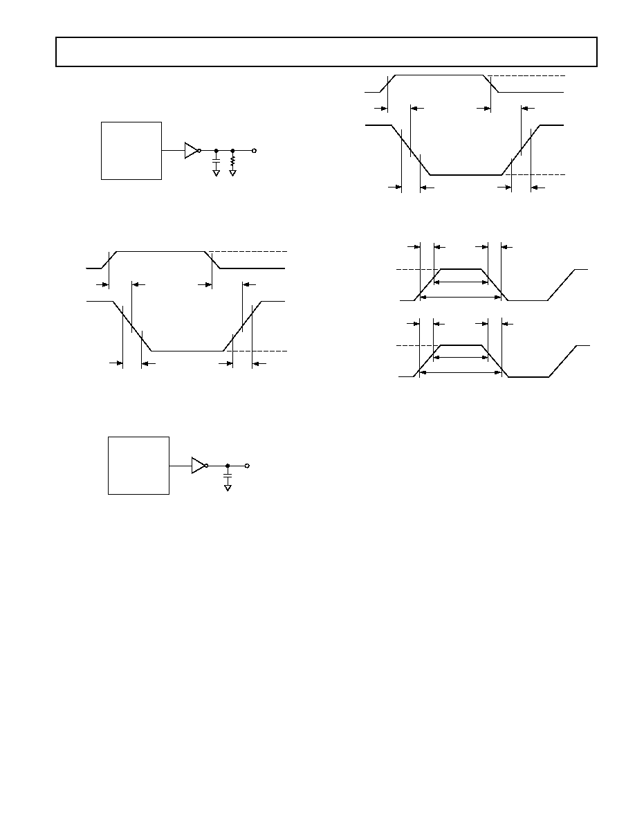
Test Circuits
PULSE
GENERATOR
V
IN
C
L
R
L
V
OUT
T
Figure 1. Test Circuit for Driver Propagation Delay and
Transition Time
V
IN
1.5V
+3V
V
OUT
3V
0V
1.5V
3V
0V
V
OL
V
OH
+3V
3V
0V
t
PHL
t
PLH
t
r
t
f
Figure 2. Driver Propagation Delay and Transition Time
Waveforms
PULSE
GENERATOR
V
IN
C
L
V
OUT
R
Figure 3. Test Circuit for Receiver Propagation Delay and
Transition Time
V
IN
1.5V
V
OUT
1.5V
1.5V
+3V
V
OL
V
OH
t
PHL
t
PLH
t
r
t
f
20%
20%
1.5V
80%
80%
3V
Figure 4. Receiver Propagation Delay and Transition Time
Waveforms
0V
3V
90%
10%
5ns
5ns
DRIVER
INPUT
10V
+10V
+3V
3V
200ns
200ns
RECEIVER
INPUT
Figure 5. Input Waveforms Used in AC Performance Tests
REV. 0
ADM2209E
6
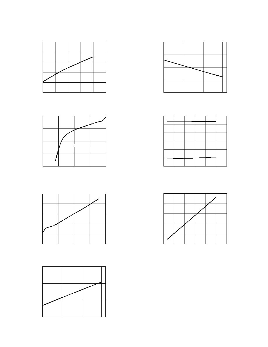
Typical Performance Curves (V
STBY
= +5 V)
LOAD CURRENT mA
4
14
10
VOLTS
6
8
10
12
0
20
30
40
50
Figure 6. V vs. Load Current
LOAD CURRENT mA
4
15
Tx OUT HIGH Volts
12
10
8
6
Tx OUTPUT VOLTAGE HIGH (V)
20
10
5
0
Figure 7. Transmitter Output Voltage High vs. Load
Current
LOAD CURRENT mA
14
5
Tx OUT LOW Volts
6
8
10
12
0
10
15
4
20
Figure 8. Transmitter Output Voltage Low vs. Load Current
V
DD
8
11.5
Tx OUT HIGH Volts
14
12
10
10.5
12.5
13.5
Figure 9. Transmitter Output Voltage High vs. V
DD
V
DD
14
11.5
Tx OUT LOW Volts
6
8
10
12
10.5
12.5
13.5
Figure 10. Transmitter Output Voltage Low vs. V
DD
LOAD CAPACITANCE pF
15
10
15
200
Tx OUT HIGH/LOW Volts
5
0
5
10
TxHI
TxLO
0
400
600
800
1000
1200
Figure 11. Transmitter Output Voltage High/Low vs.
Load Capacitance
LOAD CAPACITANCE pF
12
10
200
I
DD
mA
8
6
4
2
I
DD
0
400
600
800
1000
1200
Figure 12. I
DD
vs. Load Capacitance V
STBY
= 5 V
REV. 0
ADM2209E
7
Typical Performance Curves (V
STBY
= +3.3 V)
LOAD CURRENT mA
3
13
10
VOLTS
5
7
9
11
CHARGE PUMP VOLTAGE V (V)
0
20
30
40
50
Figure 13. V vs. Load Current
LOAD CURRENT mA
1
10
Tx OUT HIGH Volts
9
7
5
3
Tx OUTPUT VOLTAGE HIGH (V)
15
5
0
11
13
Figure 14. Transmitter Output Voltage High vs. Load
Current
LOAD CURRENT mA
12
5
Tx OUT LOW Volts
4
6
8
10
Tx OUTPUT VOLTAGE LOW (V)
0
10
15
2
Figure 15. Transmitter Output Voltage Low vs. Load
Current
V
DD
8
11.5
Tx OUT HIGH Volts
14
12
10
10.5
12.5
13.5
Figure 16. Transmitter Output Voltage High vs. V
DD
V
DD
14
11
Tx OUT LOW Volts
6
8
10
12
10
12
13
14
Figure 17. Transmitter Output Voltage Low vs. V
DD
LOAD CAPACITANCE pF
15
10
15
200
Tx OUT Volts
5
0
5
10
TxHI
TxLO
0
400
600
800
1000
1200
Figure 18. Transmitter Output Voltage vs. Load Ca-
pacitance @ 460 kBPS
LOAD CAPACITANCE pF
2
200
I
DD
mA
10
8
6
4
I
DD
mA
0
400
600
800
1000
1200
Figure 19. I
DD
vs. Load Capacitance
REV. 0
ADM2209E
8
GENERAL DESCRIPTION
The ADM2209E is a rugged dual-port RS-232 line driver/re-
ceiver that operates from a single, +12 V supply, thus removing
the need for a 12 V power supply. It contains ten receivers and
six drivers, and provides a one-chip solution for both serial ports
in desktop or portable personal computers.
Features include low power consumption, high transmission
rates and compatibility with the EU directive on electromagnetic
compatibility. EM compatibility includes protection against
radiated and conducted interference including high levels of
electrostatic discharge.
All RS-232 inputs and outputs contain protection against
electrostatic discharges up to
±
15 kV and electrical fast tran-
sients up to
±
2 kV. This ensures compliance to IE1000-4-2 and
IEC1000-4-4 requirements.
This device is ideally suited for operation in electrically harsh
environments or where RS-232 cables are frequently being
plugged/unplugged. They are also immune to high RF field
strengths without special shielding precautions. Emissions are
also controlled to within very strict limits.
A novel feature of this device is that one receiver (R5) in each
port can be kept active by a low-current, +3 V/+5 V power
supply, while the rest of the system is powered down. This al-
lows the system to be awakened when peripheral devices begin
to communicate with it.
CIRCUIT DESCRIPTION
The internal circuitry consists of four main sections. These are:
1. A charge pump dc-to-dc converter
2. Logic (3 V/5 V)-to-EIA-232 transmitters
3. EIA-232-to-logic receivers
4. Transient protection circuit on all I-O lines
Charge Pump DC-DC Converter
The dc-dc converter generates a negative supply voltage from
the +12 V supply, thus removing the need for a separate 12 V
rail. It consists of an on-chip 200 kHz oscillator, switching ma-
trix and two external capacitors, as shown in Figure 20.
+
+
INTERNAL
OSCILLATOR
GND
C2
C1
S1
S2
S3
S4
V
DD
+12V
GND
C2
Figure 20. Charge Pump DC-DC Converter
When S1 and S2 are closed, S3 and S4 are open, and C1 charges
to +12 V. S1 and S2 are then opened, while S3 and S4 are
closed to connect C1 across C2, dumping charge into C2. Since
the positive terminal of C2 is at ground, a negative voltage will
be built up on its negative terminal with each cycle of the oscil-
lator. This voltage depends on the current drawn from C2. If
the current is small, the voltage will be close to 12 V, but will
fall as the current drawn increases.
Standby Operation
The ADM2209E automatically enters a standby or shutdown
mode when the V
DD
power supply is removed. An on-chip com-
parator circuit generates an internal shutdown signal. This sig-
nal disables the internal oscillator and hence the charge pump.
The inverted output V goes to GND. All transmitter outputs
are disabled and receivers R1 through R4 on each port are three-
stated. The remaining receiver on each port (R5) remains fully
active.
The standby current I
STBY
remains less than 200
µ
A in this
mode.
V
DD
(12V)
V
STBY
(5V)
INTERNAL
SHUTDOWN SIGNAL
Figure 21. Standby Detection Circuit
Charge Pump Capacitors And Supply Decoupling
For proper operation of the charge pump, the capacitors should
have an equivalent series resistance (ESR) less than 1
. As the
charge pump draws current pulses from V
DD
, the V
DD
decou-
pling capacitor should also have low ESR. The V decoupling
capacitor and reservoir capacitor should also have low ESR
because they determine how effectively ESD pulses are clamped
to V
DD
or V by the on-chip clamp diodes. Tantalum or mono-
lithic ceramic capacitors are suitable for these components. If
using tantalum capacitors, do not forget to observe polarity.
Transmitter (Driver) Section
The drivers convert 5 V logic input levels into EIA-232 output
levels. With V
DD
= +12 V and driving an EIA-232 load, the
output voltage swing is typically
±
9 V.
Unused inputs may be left unconnected, as an internal 400 k
pull-up resistor pulls them high, forcing the outputs into a low
state. The input pull-up resistors typically source 10
µ
A when
grounded, so unused inputs should either be connected to V
STBY
or left unconnected in order to minimize power consumption.
Receiver Section
The receivers are inverting level shifters that accept EIA-232
input levels and translate them into 5 V logic output levels. The
inputs have internal 5 k
pull-down resistors to ground and are
also protected against overvoltages of up to
±
30 V. The guaran-
teed switching thresholds are 0.4 V minimum and 2.4 V maxi-
mum. Unconnected inputs are pulled to 0 V by the internal
5 k
pull-down resistor. This, therefore, results in a Logic 1
output level for unconnected inputs or for inputs connected to
GND.
The receivers have Schmitt trigger input with a hysteresis level
of 0.25 V. This ensures error-free reception for both noisy in-
puts and for inputs with slow transition times.
HIGH BAUD RATE
The ADM2209E features high slew rates permitting data trans-
mission at rates well in excess of the EIA-232-E specifications.
RS-232 levels are maintained at data rates up to 920 kb/s. This
allows for high speed data links between two terminals and,
indeed, is suitable for the new generation modem standards.
ESD/EFT TRANSIENT PROTECTION SCHEME
The ADM2209E uses protective clamping structures on all in-
puts and outputs, which clamps the voltage to a safe level and
dissipates the energy present in ESD (Electrostatic) and EFT
REV. 0
ADM2209E
9
(Electrical Fast Transient) discharges. A simplified schematic of
the protection structure is shown in Figures 22a and 22b. Each
input and output contains two back-to-back high speed clamping
diodes. During normal operation with maximum RS-232 signal
levels, the diodes have no effect as one or the other is reverse-
biased, depending on the polarity of the signal. If, however, the
voltage exceeds about
±
50 V, reverse breakdown occurs and the
voltage is clamped at this level. The diodes are large p-n junctions
designed to handle the instantaneous current surge which can
exceed several amperes.
The transmitter outputs and receiver inputs have a similar pro-
tection structure. The receiver inputs can also dissipate some of
the energy through the internal 5 k
resistor to GND as well as
through the protection diodes.
The protection structure achieves ESD protection up to
±
15 kV
and EFT protection up to
±
2 kV on all RS-232 I-O lines. The
methods used to test the protection scheme are discussed later.
R
IN
Rx
D1
D2
RECEIVER
INPUT
Figure 22a. Receiver Input Protection Scheme
Tx
TRANSMITTER
OUTPUT
D1
D2
Figure 22b. Transmitter Output Protection Scheme
ESD TESTING (IEC1000-4-2)
IEC1000-4-2 (previously 801-2) specifies compliance testing
using two coupling methods, contact discharge and air-gap
discharge. Contact discharge calls for a direct connection to the
unit being tested. Air-gap discharge uses a higher test voltage
but does not make direct contact with the unit under test. With
air discharge, the discharge gun is moved towards the unit un-
der test developing an arc across the air gap, hence the term air-
discharge. This method is influenced by humidity, temperature,
barometric pressure, distance and rate of closure of the discharge
gun. The contact-discharge method, while less realistic, is more
repeatable and is gaining acceptance in preference to the air-gap
method.
Although very little energy is contained within an ESD pulse,
the extremely fast rise time coupled with high voltages can cause
failures in unprotected semiconductors. Catastrophic destruc-
tion can occur immediately as a result of arcing or heating. Even
if catastrophic failure does not occur immediately, the device
may suffer from parametric degradation, which may result in
degraded performance. The cumulative effects of continuous
exposure can eventually lead to complete failure.
I-O lines are particularly vulnerable to ESD damage. Simply
touching or plugging in an I-O cable can result in a static dis-
charge that can damage or completely destroy the interface
product connected to the I-O port. Traditional ESD test meth-
ods such as the MIL-STD-883B method 3015.7 do not fully
test a product's susceptibility to this type of discharge. This test
was intended to test a product's susceptibility to ESD damage
during handling. Each pin is tested with respect to all other
pins. There are some important differences between the tradi-
tional test and the IEC test:
(a) The IEC test is much more stringent in terms of discharge
energy. The peak current injected is over four times greater.
(b) The current rise time is significantly faster in the IEC test.
(c) The IEC test is carried out while power is applied to the device.
It is possible that the ESD discharge could induce latch-up in the
device under test. This test is therefore more representative of a
real-world I-O discharge where the equipment is operating nor-
mally with power applied. For maximum peace of mind, however,
both tests should be performed, to ensure maximum protection
both during handling and later, during field service.
R1
R2
C1
DEVICE
UNDER TEST
HIGH
VOLTAGE
GENERATOR
ESD TEST METHOD
R2
C1
H. BODY MIL-STD-883B
1.5k
100pF
IEC1000-4-2
330
150pF
Figure 23. ESD Test Standards
100
I
PEAK
%
90
36.8
10
t
DL
t
RL
TIME t
Figure 24. Human Body Model ESD Current Waveform
100
I
PEAK
%
90
10
TIME t
30ns
60ns
0.1 TO 1ns
Figure 25. IEC1000-4-2 ESD Current Waveform
REV. 0
ADM2209E
10
The ADM2209E is tested using both of the above-mentioned
test methods. All pins are tested with respect to all other pins as
per the MIL-STD-883B specification. In addition, all I-O pins
are tested as per the IEC test specification. The products were
tested under the following conditions:
(a) Power-On--Normal Operation
(b) Power-Off
There are four levels of compliance defined by IEC1000-4-2.
The ADM2209E meets the most stringent compliance level for
both contact and air-gap discharge. This means that the products
are able to withstand contact discharges in excess of 8 kV and air-
gap discharges in excess of 15 kV.
Table IV. IEC1000-4-2 Compliance Levels
Contact Discharge
Air Discharge
Level
kV
kV
1
2
2
2
4
4
3
6
8
4
8
15
Table V. ADM2209E ESD Test Results
ESD Test Method
I-O Pins
Other Pins
MIL-STD-883B
±
15 kV
±
2.5 kV
IEC1000-4-2
Contact
±
8 kV
Air
±
15 kV
FAST TRANSIENT BURST TESTING (IEC1000-4-4)
IEC1000-4-4 (previously 801-4) covers electrical fast-transient/
burst (EFT) immunity. Electrical fast transients occur as a
result of arcing contacts in switches and relays. The tests simu-
late the interference generated when, for example, a power relay
disconnects an inductive load. A spark is generated due to the
well-known back EMF effect. In fact the spark consists of a burst
of sparks as the relay contacts separate. The voltage appearing
on the line, therefore, consists of a burst of extremely fast tran-
sient impulses. A similar effect occurs when switching on fluo-
rescent lights.
The fast transient burst test defined in IEC1000-4-4 simulates
this arcing and its waveform is illustrated in Figure 26. It con-
sists of a burst of 2.5 kHz to 5 kHz transients repeating at
300 ms intervals. It is specified for both power and data lines.
300ms
15ms
t
V
5ns
0.2/0.4ms
50ns
V
t
Figure 26. IEC1000-4-4 Fast Transient Waveform
Table VI.
V Peak (kV)
V Peak (kV)
Level
PSU
I-O
1
0.5
0.25
2
1
0.5
3
2
1
4
4
2
A simplified circuit diagram of the actual EFT generator is
illustrated in Figure 27.
R
C
R
M
C
C
HIGH
VOLTAGE
SOURCE
L
Z
S
C
D
50
OUTPUT
Figure 27. IEC1000-4-4 Fast Transient Generator
The transients are coupled onto the signal lines using an EFT
coupling clamp. The clamp is 1 meter long and it completely
surrounds the cable, providing maximum coupling capacitance
(50 pF to 200 pF typ) between the clamp and the cable. High
energy transients are capacitively coupled onto the signal lines.
Fast rise times (5 ns) as specified by the standard result in very
effective coupling. This test is very severe since high voltages
are coupled onto the signal lines. The repetitive transients can
often cause problems where single pulses do not. Destructive
latch-up may be induced due to the high energy content of the
transients. Note that this stress is applied while the interface
products are powered up and transmitting data. The EFT test
applies hundreds of pulses with higher energy than ESD. Worst
case transient current on an I-O line can be as high as 40 A.
Test results are classified according to the following:
1. Normal performance within specification limits.
2. Temporary degradation or loss of performance which is self-
recoverable.
3. Temporary degradation or loss of function or performance
which requires operator intervention or system reset.
4. Degradation or loss of function which is not recoverable due
to damage.
The ADM2209E has been tested under worst case conditions
using unshielded cables and meets Classification 2. Data trans-
mission during the transient condition is corrupted, but it may
be resumed immediately following the EFT event without user
intervention.
IEC1000-4-3 RADIATED IMMUNITY
IEC1000-4-3 (previously IEC801-3) describes the measure-
ment method and defines the levels of immunity to radiated
electromagnetic fields. It was originally intended to simulate the
electromagnetic fields generated by portable radio transceivers
or any other device that generates continuous wave radiated
electromagnetic energy. Its scope has since been broadened to
include spurious EM energy which can be radiated from fluores-
cent lights, thyristor drives, inductive loads, etc.
REV. 0
ADM2209E
11
Testing for immunity involves irradiating the device with an EM
field. There are various methods of achieving this, including use
of an echoic chamber, stripline cell, TEM cell, GTEM cell. A
stripline cell consists of two parallel plates with an electric field
developed between them. The device under test is placed within
the cell and exposed to the electric field. There are three severity
levels having field strengths ranging from 1 V to 10 V/m. Results
are classified in a fashion similar to those for IEC1000-4-4.
1. Normal operation.
2. Temporary degradation or loss of function that is self-
recoverable when the interfering signal is removed.
3. Temporary degradation or loss of function that requires
operator intervention or system reset when the interfering
signal is removed.
4. Degradation or loss of function that is not recoverable due to
damage.
The ADM2209E easily meets Classification 1 at the most strin-
gent (Level 3) requirement. In fact, field strengths up to 30 V/m
showed no performance degradation and error-free data trans-
mission continued even during irradiation.
Table VII. Test Severity Levels (IEC1000-4-3)
Field Strength
Level
V/m
1
1
2
3
3
10
EMISSIONS/INTERFERENCE
EN55 022, CISPR22 defines the permitted limits of radiated
and conducted interference from Information Technology (IT)
equipment. The objective of the standard is to minimize the
level of emissions, both conducted and radiated.
APPLICATIONS INFORMATION
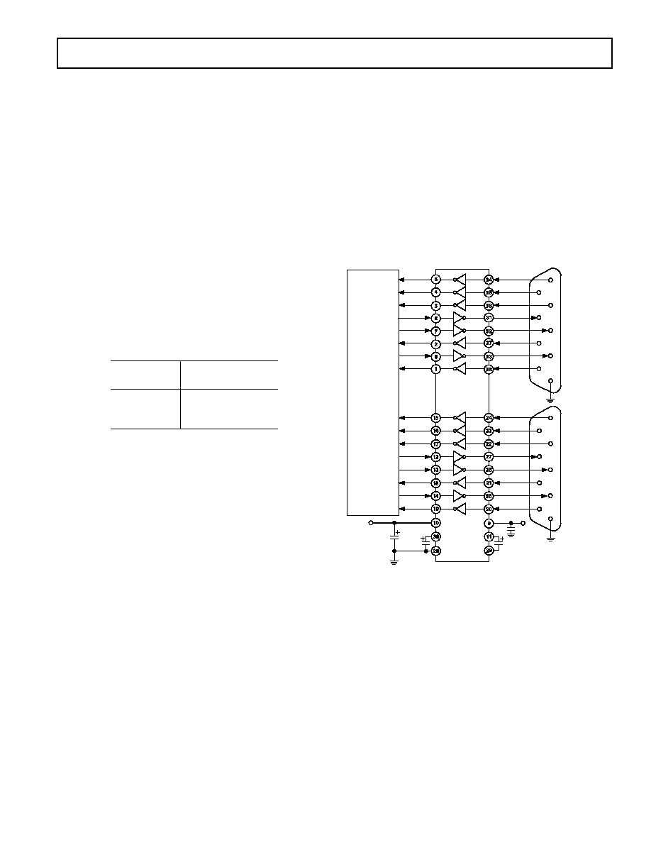
In a typical Data Terminal Equipment (DTE) to Data Circuit
Terminating Equipment (DCE) 9-lead de facto interface imple-
mentation, two data lines (TxD and RxD) and six control lines
(RTS, DTR, DSR, CTS and RI) are required. With its six
drivers and ten receivers, the ADM2209E offers a single-chip
solution for the two RS-232 ports normally supplied as standard
in a desktop or notebook personal computer, as shown in Figure
28. The flow-through pinout of the device allows for a very
simple PCB layout, and allows a ground plane to be placed
beneath the IC, and ground lines to be inserted between the
signal lines to minimize crosstalk, without the complication of
multilayer PCBs.
Note that the two receivers kept active by the standby supply
(R5
IN
A and R5
IN
B) should be connected to the Ring In (RI)
line, so that the system can be awakened when a peripheral
device begins to communicate.
FAIL-SAFE RECEIVER OUTPUTS
The ADM2209E has fail-safe receiver outputs that assume a
high output level if the receiver input is zero or open-circuit.
LAPLINK COMPATIBILITY
The ADM2209E can operate up to 460 kbps data rate under
maximum driver load conditions of C
L
= 1000 pF and
R
L
= 3 k
at minimum power supply voltages.
SUPER I/O
CHIP
DCD
DSR
RxD
RTS
TxD
CTS
DTR
RI
DCD
DSR
RxD
RTS
TxD
CTS
DTR
RI
1
2
3
4
5
6
8
9
DCD
DSR
RxD
RTS
TxD
CTS
DTR
RI
DCD
DSR
RxD
RTS
TxD
CTS
DTR
RI
0.1 F
+12V
+3V or +5V
9-WAY D
CONNECTOR
COM2
9-WAY D
CONNECTOR
COM1
7
1
2
3
4
5
6
8
9
7
R1
T3
R3
R2
T1
T2
R4
R5
T3
R3
R2
T1
T2
R4
R1
R5
ADM2209E
0.1 F
0.1 F
0.1 F
Figure 28. Typical Application for a Dual Serial Port
REV. 0
ADM2209E
12
C364287/99
PRINTED IN U.S.A.
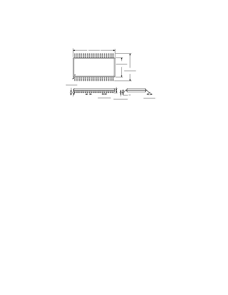
OUTLINE DIMENSIONS
Dimensions shown in inches and (mm).
38-Lead TSSOP Package (RU-38)
38
20
19
1
0.386 (9.80)
0.378 (9.60)
0.256 (6.50)
0.246 (6.25)
0.177 (4.50)
0.169 (4.30)
PIN 1
SEATING
PLANE
0.006 (0.15)
0.002 (0.05)
0.0200 (0.50)
BSC
0.0433 (1.10)
MAX
0.0106 (0.27)
0.0067 (0.17)
0.0079 (0.20)
0.0035 (0.090)
0.028 (0.70)
0.020 (0.50)
8
0