 | –≠–ª–µ–∫—Ç—Ä–æ–Ω–Ω—ã–π –∫–æ–º–ø–æ–Ω–µ–Ω—Ç: ADM241LAR | –°–∫–∞—á–∞—Ç—å:  PDF PDF  ZIP ZIP |
REV. 0
Information furnished by Analog Devices is believed to be accurate and
reliable. However, no responsibility is assumed by Analog Devices for its
use, nor for any infringements of patents or other rights of third parties
which may result from its use. No license is granted by implication or
otherwise under any patent or patent rights of Analog Devices.
a
+5 V Powered
CMOS RS-232 Drivers/Receivers
ADM223/ADM230L≠ADM241L
One Technology Way, P.O. Box 9106, Norwood, MA 02062-9106, U.S.A.
Tel: 617/329-4700
World Wide Web Site: http://www.analog.com
Fax: 617/326-8703
© Analog Devices, Inc., 1997
ADM232L TYPICAL OPERATING CIRCUIT
Table I. Selection Table
No. of
No. of
Low Power
TTL
Part
Power
RS-232
RS-232
External
Shutdown
Three-State
No. of
Number
Supply Voltage
Drivers
Receivers
Capacitors
(SD)
EN
Pins
ADM223
+5 V
4
5
4
Yes (
SD)
Yes (EN)
28
ADM230L
+5 V
5
0
4
Yes
No
20
ADM231L
+5 V & +7.5 V to +13.2 V
2
2
2
No
No
14
ADM232L
+5 V
2
2
4
No
No
16
ADM233L
+5 V
2
2
None
No
No
20
ADM234L
+5 V
4
0
4
No
No
16
ADM235L
+5 V
5
5
None
Yes
Yes
24
ADM236L
+5 V
4
3
4
Yes
Yes
24
ADM237L
+5 V
5
3
4
No
No
24
ADM238L
+5 V
4
4
4
No
No
24
ADM239L
+5 V & +7.5 V to +13.2 V
3
5
2
No
Yes
24
ADM241L
+5 V
4
5
4
Yes
Yes
28
FEATURES
Single 5 V Power Supply
Meets All EIA-232-E and V.28 Specifications
120 kB/s Data Rate
On-Board DC-DC Converters
9 V Output Swing with +5 V Supply
Small 1 F Capacitors
Low Power Shutdown
1 A
Receivers Active in Shutdown (ADM223)
ESD > 2 kV
30 V Receiver Input Levels
Latch-Up FREE
Plug-In Upgrade for MAX223/230-241
Plug-In Upgrade for AD230≠AD241
APPLICATIONS
Computers
Peripherals
Modems
Printers
Instruments
GENERAL DESCRIPTION
The ADM2xx family of line drivers/receivers is intended for all
EIA-232-E and V.28 communications interfaces, especially in
applications where
±
12 V is not available. The ADM223,
ADM230L, ADM235L, ADM236L and ADM241L feature a
low power shutdown mode that reduces power dissipation to
less than 5
µ
W, making them ideally suited for battery powered
equipment. Two receivers remain enabled during shutdown on
the ADM223. The ADM233L and ADM235L do not require
any external components and are particularly useful in applica-
tions where printed circuit board space is critical.
All members of the ADM230L family, except the ADM231L
and the ADM239L, include two internal charge pump voltage
converters that allow operation from a single +5 V supply.
These converters convert the +5 V input power to the
±
10 V
required for RS-232 output levels. The ADM231L and
ADM239L are designed to operate from +5 V and +12 V sup-
plies. An internal +12 V to ≠12 V charge pump voltage con-
verter generates the ≠12 V supply.
The ADM2xxL is an enhanced upgrade for the AD2xx family
featuring lower power consumption, faster slew rate and opera-
tion with smaller (1
µ
F) capacitors.
*INTERNAL 400k
PULL-UP RESISTOR ON EACH TTL/CMOS INPUT
**INTERNAL 5k
PULL-DOWN RESISTOR ON EACH RS-232 INPUT
+5V TO +10V
VOLTAGE
DOUBLER
+10V TO ≠10V
VOLTAGE
INVERTER
1
µ
F
16V
1
µ
F
6.3V
+5V INPUT
VCC
V+
V≠
C1+
C1≠
C2+
C2≠
ADM232L
1
µ
F
6.3V
1
µ
F
16V
6
GND
15
4
5
3
1
2
1
µ
F
6.3V
T1IN
RS-232
OUTPUTS
TTL/CMOS
INPUTS*
T1OUT
T2IN
R1OUT
R2OUT
T2OUT
R1IN
R2IN
R1
R2
T2
T1
TTL/CMOS
OUTPUTS
RS-232
INPUTS**
13
10
7
11
8
14
9
12
16
REV. 0
≠2≠
ADM223/ADM230L≠ADM241L≠SPECIFICATIONS
V
CC
= +5 V 5% (ADM230L, 33L, 35L, 37L); V+ = 7.5 V to 13.2 V (ADM231L & ADM239L); C1≠C4 = 1.0 F Ceramic. All Specifications T
MIN
to
T
MAX
unless otherwise noted.)
Parameter
Min
Typ
Max Units Test Conditions/Comments
Output Voltage Swing
±
5
±
9
Volts
All Transmitter Outputs Loaded with 3 k
to Ground
V
CC
Power Supply Current
2
3.0
mA
No Load, All T
INS
= V
CC
(Except ADM223)
3.5
6
mA
No Load, All T
INS
= GND
0.4
1
mA
ADM231L, ADM239L
V+ Power Supply Current
1.5
4
mA
No Load, V+ = 12 V ADM231L & ADM239L Only
Shutdown Supply Current
1
5
µ
A
Input Logic Threshold Low, V
INL
0.8
V
T
IN
,
EN, SD, EN, SD
Input Logic Threshold High, V
INH
2.0
V
T
IN
,
EN, SD, EN, SD
Logic Pull-Up Current
10
25
µ
A
T
IN
= 0 V
RS-232 Input Voltage Range
≠30
+30
V
RS-232 Input Threshold Low
0.8
1.2
V
RS-232 Input Threshold High
1.7
2.4
V
RS-232 Input Hysteresis
0.2
0.5
1.0
V
RS-232 Input Resistance
3
5
7
k
TTL/CMOS Output Voltage Low, V
OL
0.4
V
TTL/CMOS Output Voltage High, V
OH
3.5
V
I
OUT
= ≠1.0 mA
TTL/CMOS Output Leakage Current
0.05
±
5
µ
A
EN = V
CC
, 0 V
R
OUT
V
CC
Output Enable Time (T
EN
)
250
ns
ADM223, ADM235L, ADM236L, ADM239L, ADM241L
(Figure 25. C
L
= 150 pF)
Output Disable Time (T
DIS
)
50
ns
ADM223, ADM235L, ADM236L, ADM239L, ADM241L
(Figure 25. R
L
= 1 k
)
Propagation Delay
0.5
µ
s
RS-232 to TTL
Instantaneous Slew Rate
1
25
30
V/
µ
s
C
L
= 10 pF, R
L
= 3-7 k
, T
A
= +25
∞
C
Transition Region Slew Rate
5
V/
µ
s
R
L
= 3 k
, C
L
= 2500 pF
Measured from +3 V to ≠3 V or ≠3 V to +3 V
Output Resistance
300
V
CC
= V+ = V≠ = 0 V, V
OUT
=
±
2 V
RS-232 Output Short Circuit Current
±
10
mA
NOTE
1
Sample tested to ensure compliance.
Specifications subject to change without notice.
Thermal Impedance,
JA
N-14 DIP . . . . . . . . . . . . . . . . . . . . . . . . . . . . . . . 140
∞
C/W
N-16 DIP . . . . . . . . . . . . . . . . . . . . . . . . . . . . . . . 135
∞
C/W
N-20 DIP . . . . . . . . . . . . . . . . . . . . . . . . . . . . . . . 125
∞
C/W
N-24 DIP . . . . . . . . . . . . . . . . . . . . . . . . . . . . . . . 120
∞
C/W
N-24A DIP . . . . . . . . . . . . . . . . . . . . . . . . . . . . . 110
∞
C/W
R-16 SOIC . . . . . . . . . . . . . . . . . . . . . . . . . . . . . . 105
∞
C/W
R-20 SOIC . . . . . . . . . . . . . . . . . . . . . . . . . . . . . . 105
∞
C/W
R-24 SOIC . . . . . . . . . . . . . . . . . . . . . . . . . . . . . . . 85
∞
C/W
R-28 SOIC . . . . . . . . . . . . . . . . . . . . . . . . . . . . . . . 80
∞
C/W
RS-28 SSOP . . . . . . . . . . . . . . . . . . . . . . . . . . . . 100
∞
C/W
Q-14 Cerdip . . . . . . . . . . . . . . . . . . . . . . . . . . . . . 105
∞
C/W
Q-16 Cerdip . . . . . . . . . . . . . . . . . . . . . . . . . . . . . 100
∞
C/W
Q-20 Cerdip . . . . . . . . . . . . . . . . . . . . . . . . . . . . . 100
∞
C/W
Q-24 Cerdip . . . . . . . . . . . . . . . . . . . . . . . . . . . . . . 55
∞
C/W
D-24 Ceramic . . . . . . . . . . . . . . . . . . . . . . . . . . . . 50
∞
C/W
Operating Temperature Range
Commercial (J Version) . . . . . . . . . . . . . . . . . . . 0 to +70
∞
C
Industrial (A Version) . . . . . . . . . . . . . . . . ≠40
∞
C to +85
∞
C
Storage Temperature Range . . . . . . . . . . . ≠65
∞
C to + 150
∞
C
Lead Temperature, Soldering . . . . . . . . . . . . . . . . . . +300
∞
C
Vapour Phase (60 sec) . . . . . . . . . . . . . . . . . . . . . . +215
∞
C
Infrared (15 sec) . . . . . . . . . . . . . . . . . . . . . . . . . . . +220
∞
C
ESD Rating . . . . . . . . . . . . . . . . . . . . . . . . . . . . . . . . >2000 V
*This is a stress rating only and functional operation of the device at these or any
other conditions above those indicated in the operational sections of this specifi-
cation is not implied. Exposure to absolute maximum rating conditions for
extended periods of time may affect reliability.
V
CC
= +5 V 10% (ADM223, 31L,
32L, 34L, 36L, 38L, 39L, 41L);
ABSOLUTE MAXIMUM RATINGS*
(T
A
= 25
∞
C unless otherwise noted)
V
CC
. . . . . . . . . . . . . . . . . . . . . . . . . . . . . . . . . ≠0.3 V to +6 V
V+ . . . . . . . . . . . . . . . . . . . . . . . . . . . . (V
CC
≠ 0.3 V) to +14 V
V≠ . . . . . . . . . . . . . . . . . . . . . . . . . . . . . . . . . +0.3 V to ≠14 V
Input Voltages
T
IN
. . . . . . . . . . . . . . . . . . . . . . . . . ≠0.3 V to (V
CC
+ 0.3 V)
R
IN
. . . . . . . . . . . . . . . . . . . . . . . . . . . . . . . . . . . . . . .
±
30 V
Output Voltages
T
OUT
. . . . . . . . . . . . . . . . . . (V+, + 0.3 V) to (V≠, ≠ 0.3 V)
R
OUT
. . . . . . . . . . . . . . . . . . . . . . . ≠0.3 V to (V
CC
+ 0.3 V)
Short Circuit Duration
T
OUT
. . . . . . . . . . . . . . . . . . . . . . . . . . . . . . . . . Continuous
Power Dissipation
N-14 DIP (Derate 10 mW/
∞
C above +70
∞
C) . . . . . 800 mW
N-16 DIP (Derate 10.5 mW/
∞
C above +70
∞
C) . . . 840 mW
N-20 DIP (Derate 11 mW/
∞
C above +70
∞
C) . . . . . 890 mW
N-24 DIP (Derate 13.5 mW/
∞
C above +70
∞
C) . . 1000 mW
N-24A DIP (Derate 13.5 mW/
∞
C above +70
∞
C) . . 500 mW
R-16 SOIC (Derate 9 mW/
∞
C above +70
∞
C) . . . . . 760 mW
R-20 SOIC (Derate 9.5 mW/
∞
C above +70
∞
C) . . . 800 mW
R-24 SOIC (Derate 12 mW/
∞
C above +70
∞
C) . . . . 850 mW
R-28 SOIC (Derate 12.5 mW/
∞
C above +70
∞
C) . . 900 mW
RS-28 SSOP (Derate 10 mW/
∞
C above +70
∞
C) . . . 900 mW
Q-14 Cerdip (Derate 10 mW/
∞
C above +70
∞
C) . . . 720 mW
Q-16 Cerdip (Derate 10 mW/
∞
C above +70
∞
C) . . . 800 mW
Q-20 Cerdip (Derate 11.2 mW/
∞
C above +70
∞
C) . . . 890 mW
Q-24 Cerdip (Derate 12.5 mW/
∞
C above +70
∞
C) . . 1000 mW
D-24 Ceramic (Derate 20 mW/
∞
C above +70
∞
C) . . 1000 mW

ADM223/ADM230L≠ADM241L
≠3≠
REV. 0
ORDERING GUIDE
Temperature
Package
Temperature
Package
Temperature
Package
Model
Range
Option*
Model
Range
Option*
Model
Range
Option*
ADM223
ADM230L
ADM231L
ADM223AR
≠40
∞
C to +85
∞
C
R-28
ADM230LJN
0
∞
C to +70
∞
C
N-20
ADM231LJN
0
∞
C to +70
∞
C
N-14
ADM223ARS
≠40
∞
C to +85
∞
C
RS-28
ADM230LJR
0
∞
C to +70
∞
C
R-20
ADM231LJR
0
∞
C to +70
∞
C
R-16
ADM230LAN
≠40
∞
C to +85
∞
C
N-20
ADM231LAN
≠40
∞
C to +85
∞
C
N-14
ADM230LAR
≠40
∞
C to +85
∞
C
R-20
ADM231LAR
≠40
∞
C to +85
∞
C
R-16
ADM230LAQ
≠40
∞
C to +85
∞
C
Q-20
ADM231LAQ
≠40
∞
C to +85
∞
C
Q-14
ADM232L
ADM233L
ADM234L
ADM232LJN
0
∞
C to +70
∞
C
N-16
ADM233LJN
0
∞
C to +70
∞
C
N-20
ADM234LJN
0
∞
C to +70
∞
C
N-16
ADM232LJR
0
∞
C to +70
∞
C
R-16
ADM233LAN
≠40
∞
C to +85
∞
C
N-20
ADM234LJR
0
∞
C to +70
∞
C
R-16
ADM232LAN
≠40
∞
C to +85
∞
C
N-16
ADM234LAN
≠40
∞
C to +85
∞
C
N-16
ADM232LAR
≠40
∞
C to +85
∞
C
R-16
ADM234LAR
≠40
∞
C to +85
∞
C
R-16
ADM232LAQ
≠40
∞
C to +85
∞
C
Q-16
ADM234LAQ
≠40
∞
C to +85
∞
C
Q-16
ADM235L
ADM236L
ADM237L
ADM235LJN
0
∞
C to +70
∞
C
N-24A
ADM236LJN
0
∞
C to +70
∞
C
N-24
ADM237LJN
0
∞
C to +70
∞
C
N-24
ADM235LAN
≠40
∞
C to +85
∞
C
N-24A
ADM236LJR
0
∞
C to +70
∞
C
R-24
ADM237LJR
0
∞
C to +70
∞
C
R-24
ADM235LAQ
≠40
∞
C to +85
∞
C
D-24
ADM236LAN
≠40
∞
C to +85
∞
C
N-24
ADM237LAN
≠40
∞
C to +85
∞
C
N-24
ADM236LAR
≠40
∞
C to +85
∞
C
R-24
ADM237LAR
≠40
∞
C to +85
∞
C
R-24
ADM236LAQ
≠40
∞
C to +85
∞
C
Q-24
ADM237LAQ
≠40
∞
C to +85
∞
C
Q-24
ADM238L
ADM239L
ADM241L
ADM238LJN
0
∞
C to +70
∞
C
N-24
ADM239LJN
0
∞
C to +70
∞
C
N-24
ADM241LJR
0
∞
C to +70
∞
C
R-28
ADM238LJR
0
∞
C to +70
∞
C
R-24
ADM239LJR
0
∞
C to +70
∞
C
R-24
ADM241LAR
≠40
∞
C to +85
∞
C
R-28
ADM238LAN
≠40
∞
C to +85
∞
C
N-24
ADM239LAN
≠40
∞
C to +85
∞
C
N-24
ADM241LJRS
0
∞
C to +70
∞
C
RS-28
ADM238LAR
≠40
∞
C to +85
∞
C
R-24
ADM239LAR
≠40
∞
C to +85
∞
C
R-24
ADM241LARS ≠40
∞
C to +85
∞
C
RS-28
ADM238LAQ
≠40
∞
C to +85
∞
C
Q-24
ADM239LAQ
≠40
∞
C to +85
∞
C
Q-24
*D = Ceramic DIP; N = Plastic DIP; Q = Cerdip; R = Small Outline IC (SOIC); RS = Small Shrink Outline Package (SSOP).
CAUTION
ESD (electrostatic discharge) sensitive device. Electrostatic charges as high as 4000 V readily
accumulate on the human body and test equipment and can discharge without detection. Although
the ADM223/ADM230L≠ADM241L features proprietary ESD protection circuitry, permanent
damage may occur on devices subjected to high energy electrostatic discharges. Therefore, proper
ESD precautions are recommended to avoid performance degradation or loss of functionality.
WARNING!
ESD SENSITIVE DEVICE

ADM223/ADM230L≠ADM241L
≠4≠
REV. 0
1
2
3
4
5
6
7
8
9
10
20
19
18
17
16
15
14
13
12
11
TOP VIEW
(Not to Scale)
ADM230L
T1
IN
T2
IN
T3
IN
T4
IN
T5
IN
T1
OUT
T2
OUT
T3
OUT
T4
OUT
T5
OUT
V+
V≠
V
CC
C1+
C1≠
C2+
C2≠
GND
SD
NC
NC = NO CONNECT
Figure 1. ADM230L DIP/SOIC Pin Configuration
+5V TO +10V
VOLTAGE
DOUBLER
+10V TO ≠10V
VOLTAGE
INVERTER
12
11
10
8
13
1µF
16V
7
1µF
6.3V
+5V INPUT
V
CC
V+
V≠
C1+
C1≠
C2+
C2≠
T1
IN
NC
GND
ADM230L
SD
RS-232
OUTPUTS
TTL/CMOS
INPUTS
*
1µF
6.3V
1µF
16V
18
T1
OUT
6
*
INTERNAL 400k
PULL-UP RESISTOR ON EACH TTL/CMOS INPUT
T2
IN
T3
IN
T4
IN
T5
IN
T2
OUT
T3
OUT
T4
OUT
T5
OUT
T3
19
15
4
5
14
17
16
3
1
2
20
T4
T2
T1
T5
9
1µF
Figure 2. ADM230L Typical Operating Circuit
1
2
3
4
5
6
7
14
13
12
11
10
9
8
TOP VIEW
(Not to Scale)
ADM231L
T1
IN
T2
IN
R2
IN
R1
IN
T1
OUT
T2
OUT
R2
OUT
R1
OUT
V+
V≠
V
CC
C1+
C1≠
GND
NC
NC = NO CONNECT
1
2
3
4
5
6
7
8
16
15
14
13
12
11
10
9
TOP VIEW
(Not to Scale)
ADM231L
T1
IN
R1
IN
T1
OUT
R1
OUT
V+
V
CC
GND
T2
IN
R2
IN
T2
OUT
R2
OUT
V≠
C1+
C1≠
NC
Figure 3. ADM231L DIP & SOIC Pin Configurations
SOIC
DIP
+12V TO ≠12V
VOLTAGE
CONVERTER
2
1
3
14
V+
V≠
C+
C≠
T1
IN
ADM231L
RS-232
OUTPUTS
TTL/CMOS
INPUTS
*
1µF
16V
T1
OUT
GND
12
*
INTERNAL 400k
PULL-UP RESISTOR ON EACH TTL/CMOS INPUT
**INTERNAL 5k
PULL-DOWN RESISTOR ON EACH RS-232 INPUT
T2
IN
R1
OUT
R2
OUT
T2
OUT
R1
IN
R2
IN
1µF
16V
R1
6
7
8
9
4
10
11
5
R2
T2
T1
+7.5V TO 13.2V
TTL/CMOS
OUTPUTS
RS-232
INPUTS
**
13
+5V INPUT
V
CC
1µF
Figure 4. ADM231L Typical Operating Circuit (DIP Pinout)

ADM223/ADM230L≠ADM241L
≠5≠
REV. 0
*
INTERNAL 400k
PULL-UP RESISTOR ON EACH TTL/CMOS INPUT
**INTERNAL 5k
PULL-DOWN RESISTOR ON EACH RS-232 INPUT
+5V TO +10V
VOLTAGE
DOUBLER
+10V TO ≠10V
VOLTAGE
INVERTER
1µF
16V
1µF
6.3V
+5V INPUT
V
CC
V+
V≠
C1+
C1≠
C2+
C2≠
ADM232L
1µF
6.3V
1µF
16V
6
GND
15
4
5
3
1
2
1µF
6.3V
T1
IN
RS-232
OUTPUTS
TTL/CMOS
INPUTS
*
T1
OUT
T2
IN
R1
OUT
R2
OUT
T2
OUT
R1
IN
R2
IN
R1
R2
T2
T1
TTL/CMOS
OUTPUTS
RS-232
INPUTS
**
13
10
7
11
8
14
9
12
16
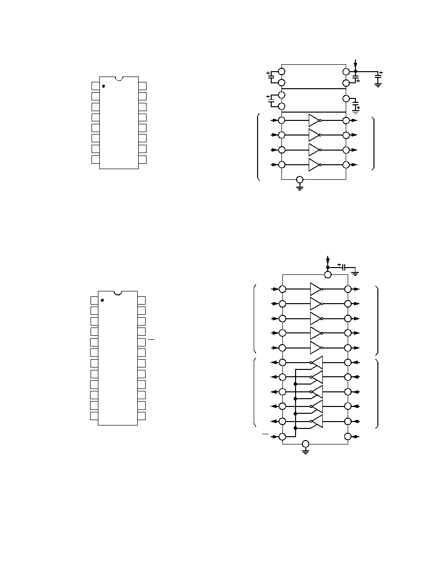
Figure 6. ADM232L Typical Operating Circuit
*
INTERNAL 400k
PULL-UP RESISTOR ON EACH TTL/CMOS INPUT
**INTERNAL 5k
PULL-DOWN RESISTOR ON EACH RS-232 INPUT
+5V INPUT
V
CC
V+
V≠
C1+
C1≠
C2+
C2≠
GND
ADM233L
7
T1
IN
RS-232
OUTPUTS
TTL/CMOS
INPUTS
*
T1
OUT
T2
IN
R1
OUT
R2
OUT
T2
OUT
R1
IN
R2
IN
R1
R2
T2
T1
TTL/CMOS
OUTPUTS
RS-232
INPUTS
**
4
1
18
2
19
5
20
3
8
13
12
17
14
11
15
10
16
V≠
C2≠
C2+
9
6
GND
DO NOT MAKE
CONNECTIONS TO
THESE PINS
INTERNAL
≠10V POWER
SUPPLY
INTERNAL
+10V POWER
SUPPLY
Figure 8. ADM233L Typical Operating Circuit
1
2
3
4
5
6
7
8
9
10
20
19
18
17
16
15
14
13
12
11
TOP VIEW
(Not to Scale)
ADM233L
R1
IN
T2
IN
R2
IN
T1
OUT
T2
OUT
R1
OUT
V+
V≠
V
CC
C1+
C2≠
C2+
C1≠
GND
GND
C2+
C2≠
R2
OUT
V≠
T1
IN
Figure 7. ADM233L DIP Pin Configuration
1
2
3
4
5
6
7
8
16
15
14
13
12
11
10
9
TOP VIEW
(Not to Scale)
ADM232L
T1
IN
R1
IN
T1
OUT
R1
OUT
V+
V
CC
GND
T2
IN
R2
IN
T2
OUT
R2
OUT
V≠
C1+
C1≠
C2≠
C2+
Figure 5. ADM232L DIP/SOIC Pin Configuration
ADM223/ADM230L≠ADM241L
≠6≠
REV. 0
T1
IN
ADM235L
SD
RS-232
OUTPUTS
TTL/CMOS
INPUTS
*
T1
OUT
GND
11
T2
IN
T3
IN
T4
IN
T5
IN
T2
OUT
T3
OUT
T4
OUT
T5
OUT
T3
22
16
7
8
15
21
19
4
2
3
1
T4
T2
T1
T5
RS-232
INPUTS
**
TTL/CMOS
OUTPUTS
R1
OUT
R1
IN
R2
IN
R3
IN
R4
IN
R5
IN
R2
OUT
R3
OUT
R4
OUT
R5
OUT
R1
R5
R4
R3
R2
20
*
INTERNAL 400k
PULL-UP RESISTOR ON EACH TTL/CMOS INPUT
**INTERNAL 5k
PULL-DOWN RESISTOR ON EACH RS-232 INPUT
EN
13
5
24
10
18
14
17
6
9
23
12
+5V INPUT
V
CC
1µF
Figure 12. ADM235L Typical Operating Circuit
+5V TO +10V
VOLTAGE
DOUBLER
+10V TO ≠10V
VOLTAGE
INVERTER
11
10
9
7
12
8
1µF
6.3V
+5V INPUT
V
CC
V+
V≠
C1+
C1≠
C2+
C2≠
T1
IN
ADM234L
RS-232
OUTPUTS
TTL/CMOS
INPUTS
*
1µF
6.3V
1µF
16V
T1
OUT
GND
5
*
INTERNAL 400k
PULL-UP RESISTOR ON EACH TTL/CMOS INPUT
T2
IN
T3
IN
T4
IN
T2
OUT
T3
OUT
T4
OUT
1µF
16V
T3
14
3
4
13
2
16
1
15
T4
T2
T1
6
1µF
Figure 10. ADM234L Typical Operating Circuit
1
2
3
4
5
6
7
8
16
15
14
13
12
11
10
9
TOP VIEW
(Not to Scale)
ADM234L
T1
IN
T3
IN
T3
OUT
V+
V
CC
GND
T2
IN
T4
IN
T1
OUT
T4
OUT
V≠
C1+
C1≠
C2≠
C2+
T2
OUT
Figure 9. ADM234L DIP/SOIC Pin Configuration
1
2
3
7
24
23
22
18
8
9
10
17
16
15
11
12
14
13
4
5
21
20
6
19
TOP VIEW
(Not to Scale)
ADM235L
T1
IN
T2
IN
T3
IN
T4
IN
T5
IN
T1
OUT
T2
OUT
T3
OUT
T4
OUT
T5
OUT
V
CC
GND
SD
EN
R3
IN
R4
IN
R5
IN
R1
IN
R2
IN
R2
OUT
R1
OUT
R3
OUT
R4
OUT
R5
OUT
Figure 11. ADM235L DIP Pin Configuration
ADM223/ADM230L≠ADM241L
≠7≠
REV. 0
T1
IN
ADM236L
SD
RS-232
OUTPUTS
TTL/CMOS
INPUTS
*
T1
OUT
GND
8
T2
IN
T3
IN
T4
IN
T2
OUT
T3
OUT
T4
OUT
T3
19
6
7
18
21
3
1
2
24
T4
T2
T1
RS-232
INPUTS
**
TTL/CMOS
OUTPUTS
R1
IN
R2
IN
R3
IN
R1
OUT
R2
OUT
R3
OUT
R3
R2
R1
20
*
INTERNAL 400k
PULL-UP RESISTOR ON EACH TTL/CMOS INPUT
**INTERNAL 5k
PULL-DOWN RESISTOR ON EACH RS-232 INPUT
EN
16
4
23
17
22
5
+5V TO +10V
VOLTAGE
DOUBLER
+10V TO ≠10V
VOLTAGE
INVERTER
14
13
12
10
15
11
1µF
6.3V
+5V INPUT
V
CC
V+
V≠
C1+
C1≠
C2+
C2≠
1µF
6.3V
1µF
16V
1µF
16V
9
1µF
Figure 14. ADM236L Typical Operating Circuit
T1
IN
ADM237L
RS-232
OUTPUTS
TTL/CMOS
INPUTS
*
T1
OUT
GND
8
T2
IN
T3
IN
T4
IN
T2
OUT
T3
OUT
T4
OUT
T3
19
6
7
18
3
1
2
24
T4
T2
T1
RS-232
INPUTS
**
TTL/CMOS
OUTPUTS
R1
IN
R2
IN
R3
IN
R1
OUT
R2
OUT
R3
OUT
R3
R2
R1
*
INTERNAL 400k
PULL-UP RESISTOR ON EACH TTL/CMOS INPUT
**INTERNAL 5k
PULL-DOWN RESISTOR ON EACH RS-232 INPUT
16
4
23
17
22
5
+5V TO +10V
VOLTAGE
DOUBLER
+10V TO ≠10V
VOLTAGE
INVERTER
14
13
12
10
15
1µF
16V
11
1µF
6.3V
+5V INPUT
V
CC
V+
V≠
C1+
C1≠
C2+
C2≠
1µF
6.3V
1µF
16V
T5
IN
T5
OUT
21
20
T5
9
1µF
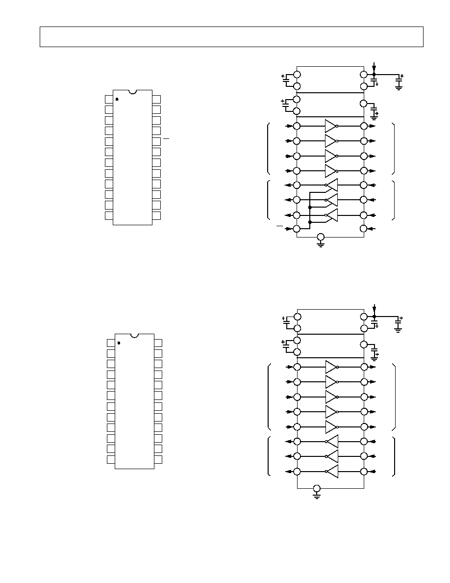
Figure 16. ADM237L Typical Operating Circuit
1
2
3
7
24
23
22
18
8
9
10
17
16
15
11
12
14
13
4
5
21
20
6
19
TOP VIEW
(Not to Scale)
ADM236L
T1
IN
T2
IN
T1
OUT
T2
OUT
T3
OUT
V
CC
GND
SD
EN
R3
IN
R1
IN
R2
IN
R2
OUT
R1
OUT
R3
OUT
T3
IN
T4
IN
T4
OUT
V+
V≠
C1+
C1≠
C2+
C2≠
Figure 13. ADM236L DIP/SOIC Pin Configuration
1
2
3
7
24
23
22
18
8
9
10
17
16
15
11
12
14
13
4
5
21
20
6
19
TOP VIEW
(Not to Scale)
ADM237L
T1
IN
T2
IN
T1
OUT
T2
OUT
T3
OUT
V
CC
GND
R3
IN
R1
IN
R2
IN
R2
OUT
R1
OUT
R3
OUT
T3
IN
T4
IN
T4
OUT
V+
V≠
C1+
C1≠
C2+
C2≠
T5
IN
T5
OUT
Figure 15. ADM237L DIP/SOIC Pin Configuration

ADM223/ADM230L≠ADM241L
≠8≠
REV. 0
T1
IN
ADM238L
RS-232
OUTPUTS
TTL/CMOS
INPUTS
*
T1
OUT
GND
8
T2
IN
T3
IN
T4
IN
T2
OUT
T3
OUT
T4
OUT
T3
19
5
18
1
2
24
T4
T2
T1
RS-232
INPUTS
**
TTL/CMOS
OUTPUTS
R1
IN
R2
IN
R3
IN
R1
OUT
R2
OUT
R3
OUT
R3
R2
R1
*
INTERNAL 400k
PULL-UP RESISTOR ON EACH TTL/CMOS INPUT
**INTERNAL 5k
PULL-DOWN RESISTOR ON EACH RS-232 INPUT
3
7
23
4
22
6
+5V TO +10V
VOLTAGE
DOUBLER
+10V TO ≠10V
VOLTAGE
INVERTER
14
13
12
10
15
1µF
16V
11
1µF
6.3V
+5V INPUT
V
CC
V+
V≠
C1+
C1≠
C2+
C2≠
1µF
6.3V
1µF
16V
21
20
9
R4
IN
R4
OUT
R4
16
17
1µF
Figure 18. ADM238L Typical Operating Circuit
T1
IN
ADM239L
NC
RS-232
OUTPUTS
TTL/CMOS
INPUTS
*
T1
OUT
GND
3
T2
IN
T3
IN
T2
OUT
T3
OUT
T3
23
24
16
15
20
13
19
T2
T1
RS-232
INPUTS
**
TTL/CMOS
OUTPUTS
R3
IN
R4
IN
R5
IN
R3
OUT
R4
OUT
R5
OUT
R5
R4
R3
14
*
INTERNAL 400k
PULL-UP RESISTOR ON EACH TTL/CMOS INPUT
**INTERNAL 5k
PULL-DOWN RESISTOR ON EACH RS-232 INPUT
EN
9
18
12
10
11
17
+12V TO ≠12V
VOLTAGE
INVERTER
7
6
8
1µF
16V
5
+5V INPUT
V
CC
V+
V≠
C1+
C1≠
1µF
16V
4
+7.5V TO +13.2V
INPUT
R1
IN
R2
IN
R1
OUT
R2
OUT
R2
R1
2
21
22
1
1µF
Figure 20. ADM239L Typical Operating Circuit
1
2
3
7
24
23
22
18
8
9
10
17
16
15
11
12
14
13
4
5
21
20
6
19
TOP VIEW
(Not to Scale)
ADM238L
T1
IN
R1
IN
T1
OUT
R2
OUT
T2
OUT
V
CC
GND
R4
IN
R2
IN
R3
IN
R3
OUT
R1
OUT
R4
OUT
T2
IN
T3
IN
T3
OUT
V+
V≠
C1+
C1≠
C2+
C2≠
T4
IN
T4
OUT
Figure 17. ADM238L DIP/SOIC Pin Configuration
1
2
3
7
24
23
22
18
8
9
10
17
16
15
11
12
14
13
4
5
21
20
6
19
TOP VIEW
(Not to Scale)
ADM239L
R4
IN
R5
IN
R1
IN
R4
OUT
R1
OUT
V
CC
GND
T3
IN
T2
IN
R2
OUT
R5
OUT
R3
OUT
R3
IN
T1
OUT
T1
IN
V+
NC
C+
C≠
T3
OUT
R2
IN
T2
OUT
V≠
EN
NC = NO CONNECT
Figure 19. ADM239L DIP/SOIC Pin Configuration
ADM223/ADM230L≠ADM241L
≠9≠
REV. 0
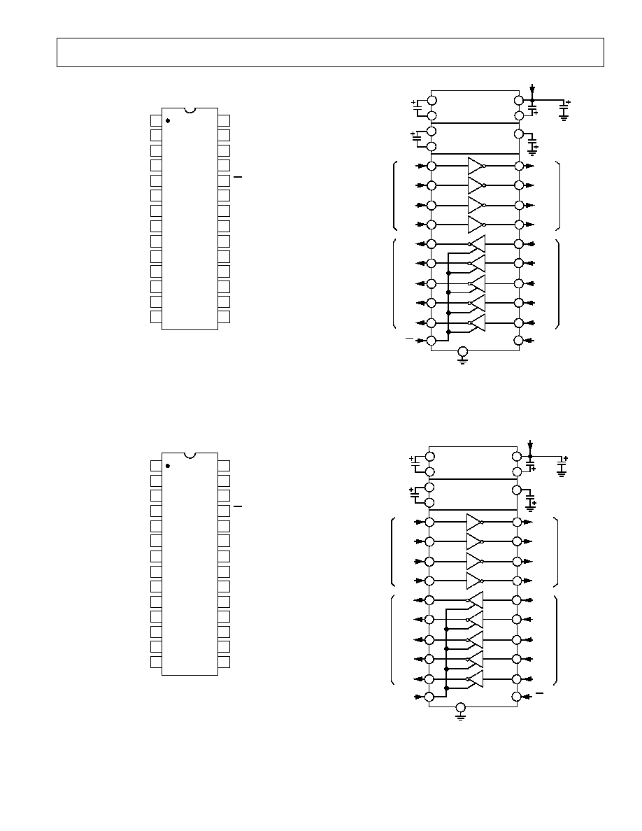
ADM241L
SD
GND
10
25
RS-232
INPUTS
**
TTL/CMOS
OUTPUTS
R3
IN
R4
IN
R5
IN
R3
OUT
R4
OUT
R5
OUT
R5
R4
R3
24
*
INTERNAL 400k
PULL-UP RESISTOR ON EACH TTL/CMOS INPUT
**INTERNAL 5k
PULL-DOWN RESISTOR ON EACH RS-232 INPUT
EN
18
27
23
19
22
26
R1
IN
R2
IN
R1
OUT
R2
OUT
R2
R1
9
4
5
8
T1
IN
RS-232
OUTPUTS
TTL/CMOS
INPUTS
*
T1
OUT
T2
IN
T3
IN
T4
IN
T2
OUT
T3
OUT
T4
OUT
T3
20
7
6
3
2
1
T4
T2
T1
+5V TO +10V
VOLTAGE
DOUBLER
+10V TO ≠10V
VOLTAGE
INVERTER
16
15
14
12
17
1
µ
F
16V
13
1
µ
F
6.3V
+5V INPUT
V
CC
V+
V≠
C1+
C1≠
C2+
C2≠
1
µ
F
16V
1
µ
F
16V
21
28
11
1
µ
F
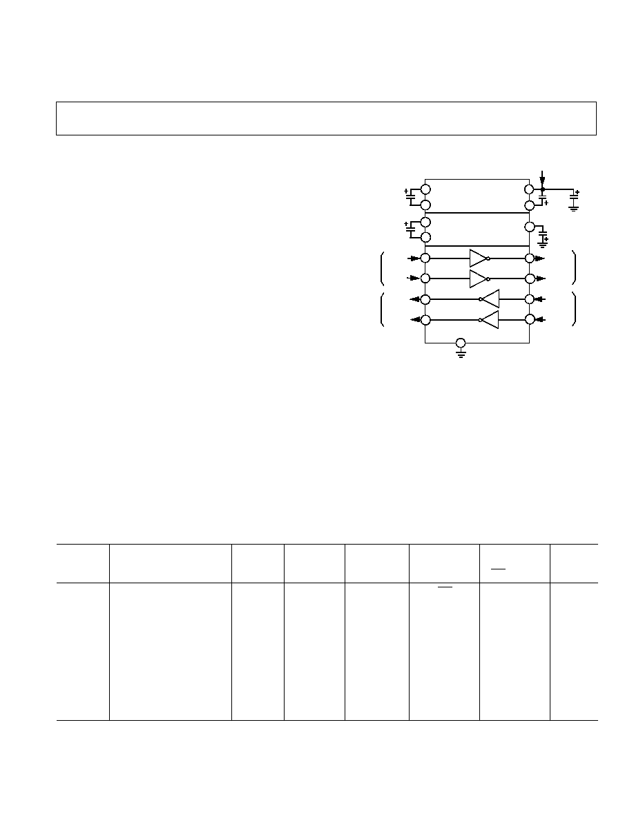
Figure 22. ADM241L Typical Operating Circuit
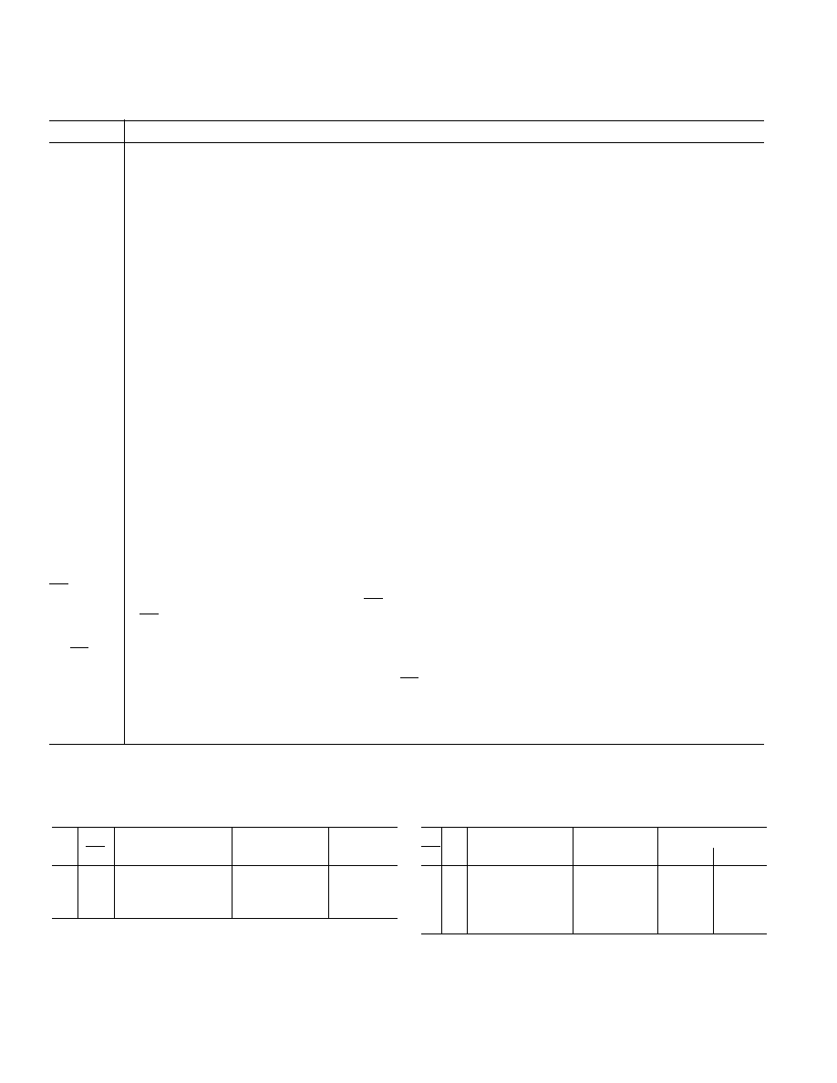
ADM223
GND
10
25
RS-232
INPUTS
**
TTL/CMOS
OUTPUTS
R3
IN
R4
IN
R5
IN
R3
OUT
R4
OUT
R5
OUT
R5
R4
R3
24
*
INTERNAL 400k
PULL-UP RESISTOR ON EACH TTL/CMOS INPUT
**INTERNAL 5k
PULL-DOWN RESISTOR ON EACH RS-232 INPUT
NOTE: RECEIVERS R4 AND R5 REMAIN ACTIVE IN SHUTDOWN.
EN
SD
18
27
23
19
22
26
R1
IN
R2
IN
R1
OUT
R2
OUT
R2
R1
9
4
5
8
T1
IN
RS-232
OUTPUTS
TTL/CMOS
INPUTS
*
T1
OUT
T2
IN
T3
IN
T4
IN
T2
OUT
T3
OUT
T4
OUT
T3
20
7
6
3
2
1
T4
T2
T1
+5V TO +10V
VOLTAGE
DOUBLER
+10V TO ≠10V
VOLTAGE
INVERTER
16
15
14
12
17
1
µ
F
16V
13
1
µ
F
6.3V
+5V INPUT
V
CC
V+
V≠
C1+
C1≠
C2+
C2≠
1
µ
F
16V
1
µ
F
16V
21
28
11
1
µ
F
Figure 24. ADM223 Typical Operating Circuit
1
2
3
7
28
27
26
22
8
9
10
21
20
19
11
12
18
17
4
5
25
24
6
23
TOP VIEW
(Not to Scale)
13
14
16
15
ADM241L
R2
OUT
R2
IN
R5
IN
T4
IN
R3
IN
T1
OUT
T2
OUT
T3
OUT
T4
OUT
R5
OUT
V+
V≠
V
CC
C1+
C1≠
C2+
C2≠
GND
SD
R3
OUT
EN
T3
IN
R4
IN
R4
OUT
R1
IN
R1
OUT
T1
IN
T2
IN
Figure 21. ADM241L SOIC/SSOP Pin Configuration
1
2
3
7
28
27
26
22
8
9
10
21
20
19
11
12
18
17
4
5
25
24
6
23
TOP VIEW
(Not to Scale)
13
14
16
15
ADM223
R2
OUT
R2
IN
R5
IN
T4
IN
R3
IN
T1
OUT
T2
OUT
T3
OUT
T4
OUT
R5
OUT
V+
V≠
V
CC
C1+
C1≠
C2+
C2≠
GND
R3
OUT
EN
SD
T3
IN
R4
IN
R4
OUT
R1
IN
R1
OUT
T1
IN
T2
IN
Figure 23. ADM223 SOIC/SSOP Pin Configuration
ADM223/ADM230L≠ADM241L
≠10≠
REV. 0
PIN FUNCTION DESCRIPTION
Mnemonic
Function
V
CC
Power Supply Input 5 V
±
10% (+5 V
±
5% ADM233L, ADM235L).
V+
Internally generated positive supply (+10 V nominal) on all parts except ADM231L and ADM239L.
ADM231L, ADM239L requires external 7.5 V to 13.2 V supply.
V≠
Internally generated negative supply (≠10 V nominal).
GND
Ground pin. Must be connected to 0 V.
C+
(ADM231L and ADM239L only). External capacitor (+ terminal) is connected to this pin.
C≠
(ADM231L and ADM239L only). External capacitor (≠ terminal) is connected to this pin.
C1+
(ADM230L, ADM232L, ADM234L, ADM236L, ADM237L, ADM238L, ADM241L) External capacitor (+ terminal)
is connected to this pin.
(ADM233L) The capacitor is connected internally and no external connection to this pin is required.
C1≠
(ADM230L, ADM232L, ADM234L, ADM236L, ADM237L, ADM238L, ADM241L) External capacitor (≠ terminal)
is connected to this pin.
(ADM233L) The capacitor is connected internally and no external connection to this pin is required.
C2+
(ADM230L, ADM232L, ADM234L, ADM236L, ADM237L, ADM238L, ADM241L) External capacitor (+ terminal)
is connected to this pin.
(ADM233L) Internal capacitor connections, Pins 11 and 15 must be connected together.
C2≠
(ADM230L, ADM232L, ADM234L, ADM236L, ADM237L, ADM238L, ADM241L) External capacitor (≠ terminal)
is connected to this pin.
(ADM233L) Internal capacitor connections, Pins 10 and 16 must be connected together.
T
IN
Transmitter (Driver) Inputs. These inputs accept TTL/CMOS levels. An internal 400 k
pull-up resistor to V
CC
is
connected on each input.
T
OUT
Transmitter (Driver) Outputs. These are RS-232 levels (typically
±
10 V).
R
IN
Receiver Inputs. These inputs accept RS-232 signal levels. An internal 5 k
pull-down resistor to GND is connected on
each input.
R
OUT
Receiver Outputs. These are TTL/CMOS levels.
EN/EN
Enable Input. Active low on ADM235L, ADM236L, ADM239L, ADM241L. Active high ADM223. This input is used
to enable/disable the receiver outputs. With
EN = low (EN = high ADM223), the receiver outputs are enabled. With
EN = high (EN = low ADM223), the outputs are placed in a high impedance state. This facility is useful for
connecting to microprocessor systems.
SD/
SD
Shutdown Input. Active high on ADM235L, ADM236L, ADM241L. Active low on ADM223. With SD = high on the
ADM235L, ADM236L, ADM241L, the charge pump is disabled, the receiver outputs are placed in a high impedance
state and the driver outputs are turned off. With
SD low on the ADM223, the charge pump is disabled, the driver
outputs are turned off and all receivers except R4 and R5 are placed in a high impedance state. In shutdown, the power
consumption reduces to 5
µ
W.
NC
No Connect. No connections are required to this pin.
Table I. ADM235L, ADM236L, ADM241L Truth Table
Transmitters
Receivers
SD
EN
Status
T1≠T5
R1≠R5
0
0
Normal Operation
Enabled
Enabled
0
1
Normal Operation
Enabled
Disabled
1
0
Shutdown
Disabled
Disabled
Table II. ADM223 Truth Table
Transmitters Receivers
SD EN Status
T1≠T4
R1≠R3
R4, R5
0
0
Shutdown
Disabled
Disabled Disabled
0
1
Shutdown
Disabled
Disabled Enabled
1
0
Normal Operation Enabled
Disabled Disabled
1
1
Normal Operation Enabled
Enabled Enabled

ADM223/ADM230L≠ADM241L
≠11≠
REV. 0
4
5.0
6
3.0
10
8
4.0
V
CC
≠ V
V
OUT
≠ V
V
OUT
(1 O/P LOADED)
V
OUT
(ALL O/Ps LOADED)
Figure 27. Transmitter Output Voltage vs. V
CC
0
40
2
0
6
4
8
10
30
20
10
| V≠ |
V
OUT
≠ V
I
OUT
-- mA
V+
Figure 25. Charge Pump V+, V≠ vs. Current
12
0
8
2
0
6
4
8
10
6
4
2
T
OUT
≠ V
T
OUT
HIGH
T
OUT
LOW
I
OUT
≠ mA
Figure 28. Transmitter Output Voltage vs. Current
18
4
2500
10
6
8
0
16
12
14
2000
1500
1000
500
CAPACITIVE LOAD ≠ pF
SLEW RATE ≠ V/µ
s
Figure 26. Transmitter Slew Rate vs. Load Capacitance
0
5
100
3
300
200
4
V
CC
≠ V
V+, V≠ IMPEDANCE ≠
V≠ (LOADED)
V≠ (UNLOADED)
V+ (UNLOADED)
V+ (LOADED)
Figure 29. Charge Pump Impedance vs. V
CC

ADM223/ADM230L≠ADM241L
≠12≠
REV. 0
10
90
100
0%
5V
0.8 V
A3
5V
5
B
L w
1ms
H
O
Figure 30. Charge Pump, V+, V≠ Exiting Shutdown
10
90
100
0%
5V
0.8 V
A3
5
B
L w
5µs
H
O
Figure 31. Transmitter Output Loaded Slew Rate
10
90
100
0%
5V
0.8 V
A3
5
B
L w
1µs
H
O
Figure 32. Transmitter Output Unloaded Slew Rate
GENERAL INFORMATION
The ADM223/ADM230L≠ADM241L family of RS-232 drivers/
receivers are designed to solve interface problems by meeting
the EIA-232-E specifications while using a single digital +5 V
supply. The EIA-232-E standard requires transmitters which
will deliver
±
5 V minimum on the transmission channel and
receivers which can accept signal levels down to
±
3 V. The
ADM223/ADM230L≠ADM241L meet these requirements by
integrating step up voltage converters and level shifting trans-
mitters and receivers onto the same chip. CMOS technology is
used to keep the power dissipation to an absolute minimum. A
comprehensive range of transmitter/receiver combinations is
available to cover most communications needs.
The ADM223, ADM230L, ADM235L, ADM236L and
ADM241L are particularly useful in battery powered systems as
they feature a low power shutdown mode which reduces power
dissipation to less than 5
µ
W.
The ADM233L and ADM235L are designed for applications
where space saving is important as the charge pump capacitors
are molded into the package.
The ADM231L and ADM239L include only a negative charge
pump converter and are intended for applications where a posi-
tive 12 V is available.
To facilitate sharing a common line or for connection to a micro-
processor data bus the ADM235L, ADM236L, ADM239L and
ADM241L feature an enable (EN, EN) function. When disabled,
the receiver outputs are placed in a high impedance state.
CIRCUIT DESCRIPTION
The internal circuitry in the ADM230L≠ADM241L consists of
three main sections. These are:
(a) A charge pump voltage converter
(b) RS-232 to TTL/CMOS receivers
(c) TTL/CMOS to RS-232 transmitters
Charge Pump DC-DC Voltage Converter
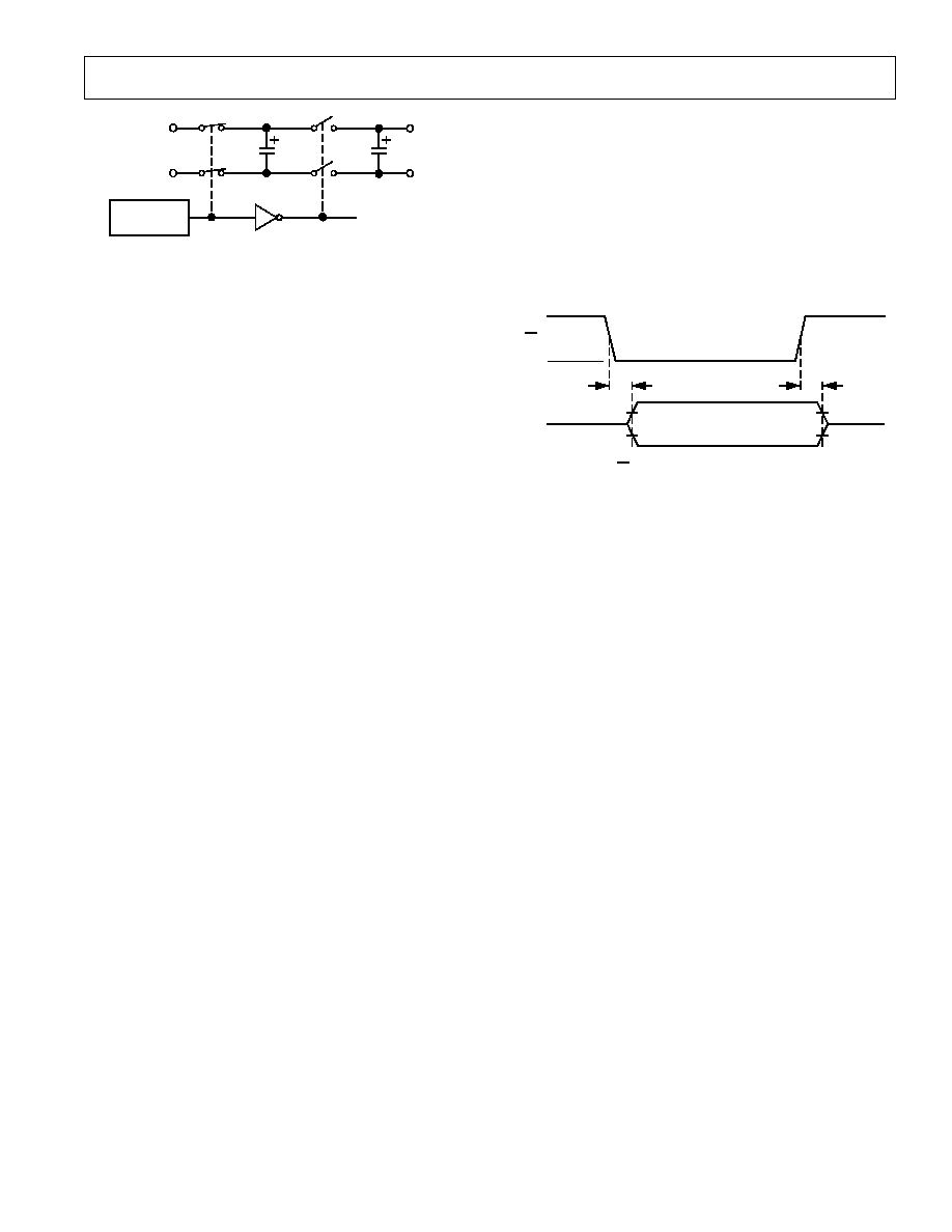
The charge pump voltage converter consists of an oscillator and
a switching matrix. The converter generates a
±
10 V supply
from the input 5 V level. This is done in two stages using a
switched capacitor technique as illustrated in Figures 33 and 34.
First, the 5 V input supply is doubled to 10 V using capacitor
C1 as the charge storage element. The 10 V level is then in-
verted to generate ≠10 V using C2 as the storage element.
S1
S3
V+ = 2V
CC
S2
S4
INTERNAL
OSCILLATOR
C1
C3
V
CC
GND
V
CC
Figure 33. Charge-Pump Voltage Doubler
ADM223/ADM230L≠ADM241L
≠13≠
REV. 0
Enable Input
The ADM235, ADM239, ADM241L and ADM223 feature an
enable input used to enable or disable the receiver outputs. The
enable input is active low on the ADM235L, ADM239L,
ADM241L and active high on the ADM223. Refer to Tables I
and II. When disabled, all receiver outputs are placed in a high
impedance state. This function allows the outputs to be con-
nected directly to a microprocessor data bus. It can also be used
to allow receivers from different devices to share a common data
line. The timing diagram for the enable function is shown in
Figure 35.
T
EN
T
DIS
3V
0V
R
OUT
3.5V
0.8V
V
OH
≠ 0.1V
V
VOL
+ 0.1V
EN*
*POLARITY OF EN IS REVERSED FOR ADM223.
Figure 35. Enable Timing
APPLICATION HINTS
Driving Long Cables
In accordance with the EIA-232-E standard, long cables are per-
missible provided that the total load capacitance does not exceed
2500 pF. For longer cables which do exceed this, then it is pos-
sible to trade off baud rate vs. cable length. Large load capaci-
tances cause a reduction in slew rate, and hence the maximum
transmission baud rate is decreased. The ADM230L-ADM241L
are designed so that the slew rate reduction with increasing load
capacitance is minimized.
For the receivers, it is important that a high level of noise immu-
nity be inbuilt so that slow rise and fall times do not cause mul-
tiple output transitions as the signal passes slowly through the
transition region. The ADM230L-ADM241L have 0.5 V of hys-
teresis to guard against this. This ensures that, even in noisy en-
vironments, error-free reception can be achieved.
High Baud Rate Operation
The ADM230L-ADM241L feature high slew rates permitting
data transmission at rates well in excess of the EIA-232-E speci-
fication. The drivers maintain
±
5 V signal levels at data rates up
to 100-kB/s under worst-case loading conditions.
S1
S3
S2
S4
INTERNAL
OSCILLATOR
C2
C4
V≠ = ≠ (V+)
GND
V+
GND
FROM
VOLTAGE
DOUBLER
Figure 34. Charge-Pump Voltage Inverter
Capacitors C3 and C4 are used to reduce the output ripple.
Their values are not critical and can be reduced if higher levels
of ripple are acceptable. The charge pump capacitors C1 and
C2 may also be reduced at the expense of higher output imped-
ance on the V+ and V≠ supplies.
The V+ and V≠ supplies may also be used to power external cir-
cuitry if the current requirements are small.
Transmitter (Driver) Section
The drivers convert TTL/CMOS input levels into EIA-232-E
output levels. With V
CC
= +5 V and driving a typical EIA-232-E
load, the output voltage swing is
±
9 V. Even under worst case
conditions the drivers are guaranteed to meet the
±
5 V
EIA-232-E minimum requirement.
The input threshold levels are both TTL and CMOS compat-
ible with the switching threshold set at V
CC
/4. With a nominal
V
CC
= 5 V the switching threshold is 1.25 V typical. Unused in-
puts may be left unconnected, as an internal 400 k
pull-up re-
sistor pulls them high forcing the outputs into a low state.
As required by the EIA-232-E standard, the slew rate is limited
to less than 30 V/
µ
s without the need for an external slew limit-
ing capacitor and the output impedance in the power-off state is
greater than 300
.
Receiver Section
The receivers are inverting level shifters which accept EIA-
232-E input levels (
±
5 V to
±
15 V) and translate them into 5 V
TTL/CMOS levels. The inputs have internal 5 k
pull-down
resistors to ground and are also protected against overvoltages of
up to
±
30 V. The guaranteed switching thresholds are 0.8 V
minimum and 2.4 V maximum which are well within the
±
3 V
EIA-232-E requirement. The low level threshold is deliberately
positive as it ensures that an unconnected input will be inter-
preted as a low level.
The receivers have Schmitt trigger inputs with a hysteresis level
of 0.5 V. This ensures error-free reception for both noisy inputs
and for inputs with slow transition times.
Shutdown (SD)
The ADM223, ADM230L, ADM235L, ADM236L and
ADM241L feature a control input that may be used to disable
the part and reduce the power consumption to less than 5
µ
W.
This is very useful in battery operated systems. During shut-
down the charge pump is turned off, the transmitters are dis-
abled and all receivers except R4 and R5 on the ADM223 are
put into a high-impedance disabled state. Receivers R4 and R5
on the ADM223 remain enabled during shutdown. This feature
allows monitoring external activity such as ring indicator moni-
toring while the device is in a low power shutdown mode.
The shutdown control input is active high on all parts except the
ADM223 where it is active low. Refer to Tables I and II.

ADM223/ADM230L≠ADM241L
≠14≠
REV. 0
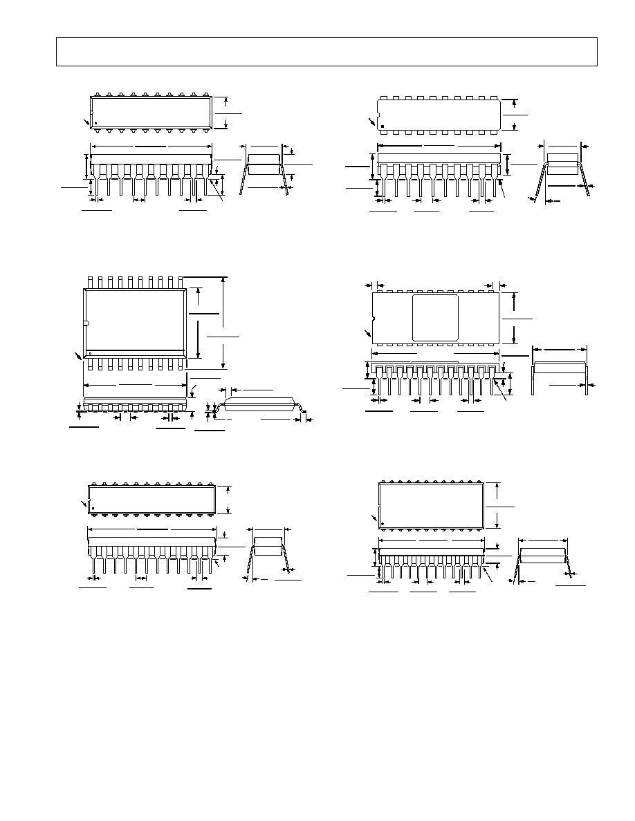
OUTLINE DIMENSIONS
Dimensions shown in inches and (mm).
14-Lead Plastic DIP (N-14)
0.325 (8.25)
0.300 (7.62)
0.015 (0.381)
0.008 (0.204)
0.195 (4.95)
0.115 (2.93)
0.210
(5.33)
0.200 (5.05)
0.125 (3.18)
0.795 (20.19)
0.725 (18.42)
0.022 (0.558)
0.014 (0.356)
0.100
(2.54)
BSC
0.070 (1.77)
0.045 (1.15)
SEATING
PLANE
0.060 (1.52)
0.015 (0.38)
0.150
(3.81)
PIN 1
0.280 (7.11)
0.240 (6.10)
7
8
14
1
16-Lead Plastic DIP (N-16)
0.325 (8.25)
0.300 (7.62)
0.015 (0.381)
0.008 (0.204)
0.195 (4.95)
0.115 (2.93)
PIN 1
0.280 (7.11)
0.240 (6.10)
9
16
1
8
0.840 (21.33)
0.745 (18.93)
0.210
(5.33)
0.200 (5.05)
0.125 (3.18)
0.022 (0.558)
0.014 (0.356)
0.100
(2.54)
BSC
SEATING
PLANE
0.060 (1.52)
0.015 (0.38)
0.150
(3.81)
0.070 (1.77)
0.045 (1.15)
16-Lead SOIC (R-16)
PIN 1
0.299 (7.60)
0.291 (7.40)
0.419 (10.65)
0.404 (10.26)
1
16
9
8
0.018 (0.46)
0.014 (0.36)
0.050 (1.27)
BSC
0.107 (2.72)
0.089 (2.26)
0.413 (10.50)
0.348 (10.10)
0.010 (0.25)
0.004 (0.10)
0.015 (0.38)
0.007 (1.18)
0.045 (1.15)
0.020 (0.50)
0.364 (9.246)
0.344 (8.738)
14-Lead Cerdip (Q-14)
0.300 (7.62)
REF
0.012 (0.305)
0.008 (0.203)
15
∞
0
∞
PIN 1
0.271 (6.89)
0.240 (6.09)
7
8
1
14
0.780 (19.81)
0.02 (0.5)
0.016 (0.406)
0.06 (1.52)
0.05 (1.27)
0.125
(3.17)
MIN
0.11 (2.79)
0.099 (2.28)
SEATING
PLANE
0.163 (4.14)
0.133 (3.378)
0.21 (5.33)
0.15 (3.81)
16-Lead Cerdip (Q-16)
15
∞
0
∞
0.300 (7.62)
REF
0.012 (0.305)
0.008 (0.203)
PIN 1
1
8
9
16
0.271 (6.89)
0.240 (6.09)
0.780 (19.81)
0.02 (0.5)
0.016 (0.406)
0.06 (1.52)
0.05 (1.27)
0.125
(3.17)
MIN
0.11 (2.79)
0.099 (2.28)
SEATING
PLANE
0.163 (4.14)
0.133 (3.378)
0.21 (5.33)
0.15 (3.81)
ADM223/ADM230L≠ADM241L
≠15≠
REV. 0
20-Lead Plastic DIP (N-20)
0.325 (8.25)
0.300 (7.62)
0.015 (0.381)
0.008 (0.204)
0.195 (4.95)
0.115 (2.93)
PIN 1
0.280 (7.11)
0.240 (6.10)
20
1
11
10
0.210
(5.33)
0.200 (5.05)
0.125 (3.18)
0.022 (0.558)
0.014 (0.356)
0.100
(2.54)
BSC
0.070 (1.78)
0.045 (1.15)
SEATING
PLANE
0.060 (1.52)
0.015 (0.38)
0.150
(3.81)
1.060 (26.90)
0.925 (23.50)
20-Lead SOIC (R-20)
PIN 1
0.2992 (7.60)
0.2914 (7.40)
0.4193 (10.65)
0.3937 (10.00)
1
20
11
10
0.0125 (0.32)
0.0091 (0.23)
0.0500 (1.27)
0.0157 (0.40)
8
∞
0
∞
0.0291 (0.74)
0.0098 (0.25)
x 45
∞
0.5118 (13.00)
0.4961 (12.60)
0.0192 (0.49)
0.0138 (0.35)
0.0500
(1.27)
BSC
0.0118 (0.30)
0.0040 (0.10)
0.1043 (2.65)
0.0926 (2.35)
24-Lead Plastic DIP (N-24)
PIN 1
0.260 ± 0.001
(6.61 ± 0.03)
24
1
13
12
0.32 (8.128)
0.30 (7.62)
0.011 (0.28)
0.009 (0.23)
15
∞
0
0.02 (0.5)
0.016 (0.41)
0.130 (3.30)
0.128 (3.25)
0.07 (1.78)
0.05 (1.27)
SEATING
PLANE
1.228 (31.19)
1.226 (31.14)
0.11 (2.79)
0.09 (2.28)
NOTES
1. LEAD NO. 1 IDENTIFIED BY DOT OR NOTCH
2. PLASTIC LEADS WILL BE EITHER SOLDER DIPPED OR TIN PLATED
IN ACCORDANCE WITH MIL-M-38510 REQUIREMENTS.
20-Lead Cerdip (Q-20)
0.32 (8.128)
0.29 (7.366)
0.011 (0.28)
0.009 (0.23)
15
∞
0
∞
PIN 1
0.28 (7.11)
0.24 (6.1)
10
11
1
20
0.97 (24.64)
0.935 (23.75)
0.15 (3.8)
0.125 (3.18)
0.02 (0.5)
0.016 (0.41)
0.07 (1.78)
0.05 (1.27)
0.11 (2.79)
0.09 (2.28)
0.18 (4.57)
0.125 (3.18)
SEATING
PLANE
0.20 (5.0)
0.14 (3.56)
LEAD NO. 1 IDENTIFIED BY DOT OR NOTCH
24-Lead Ceramic DIP (D-24)
0.015 (0.38)
0.008 (0.20)
0.620 (15.75)
0.590 (14.99)
0.005 (0.13)
PIN 1
0.098 (2.49)
0.610 (15.49)
0.500 (12.70)
13
12
24
1
0.225
(5.72)
0.023 (0.58)
0.014 (0.36)
0.070 (1.78)
0.030 (0.76)
0.150
(3.81)
SEATING
PLANE
0.110 (2.79)
0.090 (2.29)
0.075 (1.91)
0.015 (0.38)
0.200 (5.08)
0.120 (3.05)
1.290 (32.77)
24-Lead Plastic DIP (N-24A)
PIN 1
0.55 (13.97)
0.53 (13.47)
24
1
13
12
0.606 (15.4)
0.594 (15.09)
0.012 (0.305)
0.008 (0.203)
15
∞
0
∞
0.16 (4.07)
0.14 (3.56)
0.2
(5.08)
MAX
0.065 (1.66)
0.045 (1.15)
0.105 (2.67)
0.095 (2.42)
1.25 (31.75)
1.24 (31.5)
0.02 (0.508)
0.015 (0.381)
0.175
(4.45)
0.12 (3.05)
SEATING
PLANE

C1900≠18≠4/94
PRINTED IN U.S.A.
24-Lead Cerdip (Q-24)
PIN 1
1
24
12
13
1
0.295 (7.493)
MAX
SEATING
PLANE
0.225
(5.715)
MAX
0.125
(3.175)
MIN
0.070 (1.778)
0.020 (0.508)
0.180
(4.572)
MAX
1.290 (32.77) MAX
0.021 (0.533)
0.015 (0.381)
TYP
0.065 (1.651)
0.055 (1.397)
TYP
0.110 (2.794)
0.090 (2.286)
TYP
0.320 (8.128)
0.290 (7.366)
15
∞
0
∞
0.012 (0.305)
0.008 (0.203)
TYP
1. LEAD NO. 1 IDENTIFIED BY DOT OR NOTCH.
2. CERDIP LEADS WILL BE EITHER TIN PLATED OR SOLDER DIPPED
IN ACCORDANCE WITH MIL-M-38510 REQUIREMENTS.
24-Lead SOIC (R-24)
0.013 (0.32)
0.009 (0.23)
0.042 (1.067)
0.018 (0.447)
6
∞
0
∞
0.03 (0.76)
0.02 (0.51)
PIN 1
0.299 (7.6)
0.291 (7.39)
0.414 (10.52)
0.398 (10.10)
13
12
1
24
1. LEAD NO. 1 IDENTIFIED BY A DOT.
2. SOIC LEADS WILL BE EITHER TIN PLATED OR SOLDER DIPPED
IN ACCORDANCE WITH MIL-M-38510 REQUIREMENTS
0.019 (0.49)
0.014 (0.35)
0.05 (1.27)
BSC
0.096 (2.44)
0.089 (2.26)
0.608 (15.45)
0.596 (15.13)
0.01 (0.254)
0.006 (0.15)
28-Lead SOIC (R-28)
0.019 (0.49)
0.014 (0.35)
0.05 (1.27)
BSC
0.708 (18.02)
0.696 (17.67)
0.01 (0.254)
0.006 (0.15)
0.096 (2.44)
0.089 (2.26)
0.013 (0.32)
0.009 (0.23)
0.042 (1.067)
0.018 (0.457)
6
∞
0
∞
0.03 (0.76)
0.02 (0.51)
PIN 1
0.299 (7.6)
0.291 (7.39)
0.414 (10.52)
0.398 (10.10)
15
14
1
28
1. LEAD NO. IDENTIFIED BY A DOT.
2. SOICLEADS WILL BE EITHER TIN PLATED OR SOLDER DIPPED
IN ACCORDANCE WITH MIL-M-38510 REQUIREMENTS.
28-Lead SSOP (RS-28)
1. LEAD NO. 1 IDENTIFIED BY A DOT.
2. LEADS WILL BE EITHER TIN PLATED OR SOLDER DIPPED
IN ACCORDANCE WITH MIL-M-38510 REQUIREMENTS
0.009 (0.229)
0.005 (0.127)
0.037 (0.94)
0.022 (0.559)
8
∞
0
∞
0.0256 (0.65)
BSC
0.407 (10.34)
0.397 (10.08)
0.008 (0.203)
0.002 (0.050)
0.07 (1.78)
0.066 (1.67)
PIN 1
15
14
1
28
0.311 (7.9)
0.301 (7.64)
0.212 (5.38)
0.205 (5.207)
≠16≠