 | ÐлекÑÑоннÑй компоненÑ: ADM2483 | СкаÑаÑÑ:  PDF PDF  ZIP ZIP |
Äîêóìåíòàöèÿ è îïèñàíèÿ www.docs.chipfind.ru
Half-Duplex
iCoupler
®
Isolated RS-485 Transceiver
ADM2483
Rev. 0
Information furnished by Analog Devices is believed to be accurate and reliable.
However, no responsibility is assumed by Analog Devices for its use, nor for any
infringements of patents or other rights of third parties that may result from its use.
Specifications subject to change without notice. No license is granted by implication
or otherwise under any patent or patent rights of Analog Devices. Trademarks and
registered trademarks are the property of their respective owners.
One Technology Way, P.O. Box 9106, Norwood, MA 02062-9106, U.S.A.
Tel: 781.329.4700
www.analog.com
Fax: 781.326.8703
© 2004 Analog Devices, Inc. All rights reserved.
FEATURES
RS-485 transceiver with electrical data isolation
Complies with ANSI TIA/EIA RS-485-A-1998 and
ISO 8482:1987(E)
500 kbps data rate
Slew ratelimited driver outputs
Low power operation: 2.5 mA max
Suitable for 5 V or 3 V operation (V
DD1
)
High common-mode transient immunity: >25 kV/s
True fail-safe receiver inputs
Glitch-free power-up/-down protection
256 nodes on bus
Thermal shutdown protection
Safety and regulatory approvals:
UL recognition: 2500 V
RMS
for 1 minute per UL 1577
CSA Component Acceptance Notice #5A
VDE Certificate of Conformity
DIN EN 60747-5-2 (VDE 0884 Rev. 2): 2003-01
DIN EN 60950 (VDE 0805): 2001-12; EN 60950: 2000
V
IORM
= 560 V peak
Operating temperature range: -40°C to +85°C
APPLICATIONS
Low power RS-485/RS-422 networks
Isolated interfaces
Building control networks
Multipoint data transmission systems
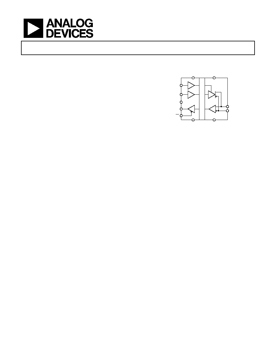
FUNCTIONAL BLOCK DIAGRAM
DE
V
DD1
GND
1
GND
2
V
DD2
TxD
POWER_VALID
RxD
RE
GALVANIC ISOLATION
A
B
04736-
001
ADM2483
Figure 1.
GENERAL DESCRIPTION
The ADM2483 differential bus transceiver is an integrated,
galvanically isolated component designed for bidirectional data
communication on balanced, multipoint bus transmission lines.
It complies with ANSI TIA/EIA RS-485-A and ISO
8482:1987(E). Using Analog Devices' iCoupler
®
technology, the
ADM2483 combines a 3-channel isolator, a 3-state differential
line driver, and a differential input receiver into a single
package. The logic side of the device is powered with either a
5 V or 3 V supply, while the bus side uses a 5 V supply only.
The ADM2483 is slew-limited to reduce reflections with
improperly terminated transmission lines. The controlled slew
rate limits the data rate to 500 kbps. The device's input
impedance is 96 k, allowing up to 256 transceivers on the bus.
Its driver has an active-high enable. The driver differential
outputs and receiver differential inputs are connected internally
to form a differential I/O port. When the driver is disabled or
when V
DD1
or V
DD2
= 0, this imposes minimal loading on the
bus. An active-high receiver disable, which causes the receive
output to enter a high impedance state, is provided as well.
The receiver inputs have a true fail-safe feature that ensures a
logic-high receiver output level when the inputs are open or
shorted. This guarantees that the receiver outputs are in a
known state before communication begins and at the point
when communication ends.
Current limiting and thermal shutdown features protect against
output short circuits and bus contention situations that might
cause excessive power dissipation. The part is fully specified
over the industrial temperature range and is available in a
16-lead wide body SOIC package.

ADM2483
Rev. 0 | Page 2 of 20
TABLE OF CONTENTS
Specifications..................................................................................... 3
Timing Specifications....................................................................... 4
Absolute Maximum Ratings............................................................ 5
ESD Caution.................................................................................. 5
Package Characteristics ............................................................... 6
Regulatory Information............................................................... 6
Insulation and Safety-Related Specifications............................ 6
VDE 0884 Insulation Characteristics
,
....................................... 7
Pin Configurations and Function Descriptions ........................... 8
Test Circuits....................................................................................... 9
Switching Characteristics .............................................................. 10
Typical Performance Characteristics ........................................... 11
Circuit Description......................................................................... 14
Electrical Isolation...................................................................... 14
Truth Tables................................................................................. 15
Power-Up/Power-Down Characteristics................................. 15
Thermal Shutdown .................................................................... 15
True Fail-Safe Receiver Inputs .................................................. 15
Magnetic Field Immunity.......................................................... 15
Applications Information .............................................................. 17
Power_Valid Input ..................................................................... 17
Isolated Power Supply Circuit .................................................. 17
Outline Dimensions ....................................................................... 18
Ordering Guide .......................................................................... 18
REVISION HISTORY
10-04--Revision 0: Initial Version
ADM2483
Rev. 0 | Page 3 of 20
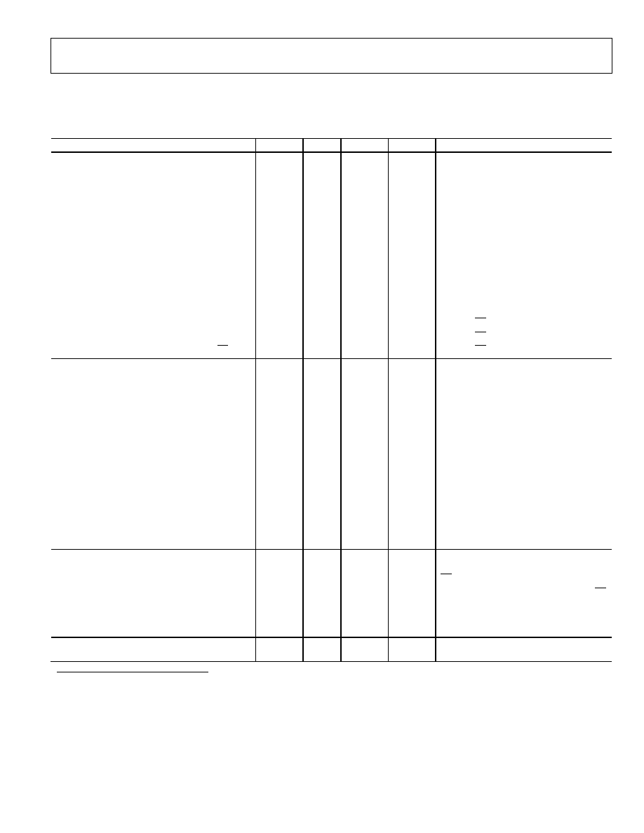
SPECIFICATIONS
2.7 V
DD1
5.5 V, 4.75 V V
DD2
5.25 V, T
A
= T
MIN
to T
MAX
, unless otherwise noted.
Table 1.
Parameter Min
Typ
Max
Unit
Test
Conditions/Comments
DRIVER
Differential Outputs:
Differential Output Voltage, V
OD
5
V
R = , Figure 3
2.0
5
V
R = 50 (RS-422), Figure 3
1.5
5
V
R = 27 (RS-485), Figure 3
1.5
5
V
V
TST
= -7 V to 12 V, V
DD1
4.75,
Figure 4
|V
OD
| for Complementary Output States
0.2
V
R = 27 or 50 , Figure 3
Common-Mode Output Voltage, V
OC
3
V
R = 27 or 50 , Figure 3
|V
OC
| for Complementary Output States
0.2
V
R = 27 or 50 , Figure 3
Output Short-Circuit Current, V
OUT
= High
-250
+250
mA
-7 V V
OUT
+ 12 V
Output Short-Circuit Current, V
OUT
= Low
-250
+250
mA
-7 V V
OUT
+ 12 V
Logic Inputs:
Input High Voltage
0.7 V
DD1
V
TxD, DE, RE, PV
Input Low Voltage
0.25 V
DD1
V
TxD, DE, RE, PV
CMOS Logic Input Current (TxD, DE, RE, PV)
-10 +0.01 +10
µA TxD, DE, RE, PV = V
DD1
or 0 V
RECEIVER
Differential Inputs:
Differential Input Threshold Voltage, V
TH
-200
-125
-30
mV
-7 V V
CM
+12 V
Input Hysteresis
20
mV
-7 V V
CM
+12 V
Input Resistance (A, B)
96
150
k
-7 V V
CM
+12 V
Input Current (A, B)
0.125
mA
V
IN
= +12 V
-0.1
mA
V
IN
= -7 V
RxD Logic Output:
Output High Voltage
V
DD1
-0.1
V I
OUT
= 20 µA, V
A
- V
B
= 0.2 V
V
DD1
-0.4
V
DD1
-0.2
V
I
OUT
= 4 mA, V
A
- V
B
= 0.2 V
Output Low Voltage
0.1
V
I
OUT
= -20 µA, V
A
- V
B
= -0.2 V
0.4
V
I
OUT
= -4 mA, V
A
- V
B
= -0.2 V
Output Short-Circuit Current
7
85
mA
V
OUT
= GND or V
CC
Three-State Output Leakage Current
±1
µA
0.4 V V
OUT
2.4 V
POWER SUPPLY CURRENT
Logic Side
2.5
mA
4.5 V V
DD1
5.5 V, Outputs Unloaded,
RE = 0 V
1.3
mA
2.7 V V
DD1
3.3 V, Outputs Unloaded, RE
= 0 V
Bus Side
2.0
mA
Outputs Unloaded, DE = 5 V
1.7
mA
Outputs Unloaded, DE = 0 V
COMMON-MODE TRANSIENT IMMUNITY
1
25 kV/µs
T × D = V
DD1
or 0 V, V
CM
= 1 kV, Transient
Magnitude = 800 V
1
Common-mode transient immunity is the maximum common-mode voltage slew rate that can be sustained while maintaining specification-compliant operation. V
CM
is the common-mode potential difference between the logic and bus sides. The transient magnitude is the range over which the common mode is slewed. The
common-mode voltage slew rates apply to both rising and falling common-mode voltage edges.

ADM2483
Rev. 0 | Page 4 of 20
TIMING SPECIFICATIONS
2.7 V
DD1
5.5 V, 4.75 V V
DD2
5.25 V, T
A
= T
MIN
to T
MAX
, unless otherwise noted.
Table 2.
Parameter Min
Typ
Max
Units
Test
Conditions/Comments
DRIVER
Maximum Data Rate
500
kbps
Propagation Delay, t
PLH
, t
PHL
250 620 ns R
LDIFF
= 54 , C
L1
= C
L2
= 100 pF, Figure 5 and Figure 9
Skew, t
SKEW
40 ns
R
LDIFF
= 54 , C
L1
= C
L2
= 100 pF, Figure 5 and Figure 9
Rise/Fall Time, t
R
, t
F
200
600
ns
R
LDIFF
= 54 , C
L1
= C
L2
= 100 pF, Figure 5 and Figure 9
Enable Time
1050
ns
R
L
= 500 , C
L
= 100 pF, Figure 6 and Figure 11
Disable Time
1050
ns
R
L
= 500 , C
L
= 15 pF, Figure 6 and Figure 11
RECEIVER
Propagation Delay, t
PLH
, t
PHL
400 1050 ns C
L
= 15 pF, Figure 7 and Figure 10
Differential Skew, t
SKEW
250
ns
C
L
= 15 pF, Figure 7 and Figure 10
Enable Time
25
70
ns
R
L
= 1 k, C
L
= 15 pF, Figure 8 and Figure 12
Disable Time
40
70
ns
R
L
= 1 k, C
L
= 15 pF, Figure 8 and Figure 12
POWER VALID INPUT
Enable Time
1
2
µs
Disable Time
3
5
µs
ADM2483
Rev. 0 | Page 5 of 20
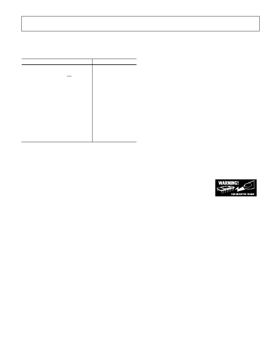
ABSOLUTE MAXIMUM RATINGS
T
A
= 25°C, unless otherwise noted. All voltages are relative to their respective ground.
Table 3.
Parameter
Rating
V
DD1
-0.5 V to +7 V
V
DD2
-0.5 V to +6 V
Digital Input Voltage (DE, RE, T × D)
-0.5 V to V
DD1
+0.5 V
Digital Output Voltage
R × D
-0.5 V to V
DD1
+0.5 V
Driver Output/Receiver Input Voltage
-9 V to +14 V
Operating Temperature Range
-40°C to +85°C
Storage Temperature Range
-55°C to +150°C
Average Output Current per Pin
-35 mA to +35 mA
JA
Thermal Impedance
73°C/W
Lead Temperature
Soldering (10 s)
260°C
Vapor Phase (60 s)
215°C
Infrared (15 s)
220°C
Stresses above those listed under Absolute Maximum Ratings
may cause permanent damage to the device. This is a stress
rating only and functional operation of the device at these or
any other conditions above those indicated in the operational
section of this specification is not implied. Exposure to absolute
maximum rating conditions for extended periods may affect
device reliability.
ESD CAUTION
ESD (electrostatic discharge) sensitive device. Electrostatic charges as high as 4000 V readily accumulate on
the human body and test equipment and can discharge without detection. Although this product features
proprietary ESD protection circuitry, permanent damage may occur on devices subjected to high energy
electrostatic discharges. Therefore, proper ESD precautions are recommended to avoid performance
degradation or loss of functionality.
Document Outline