 | ÐлекÑÑоннÑй компоненÑ: ADM3485E | СкаÑаÑÑ:  PDF PDF  ZIP ZIP |
Äîêóìåíòàöèÿ è îïèñàíèÿ www.docs.chipfind.ru
a
ADM3485E
One Technology Way, P.O. Box 9106, Norwood, MA 02062-9106, U.S.A.
Tel: 781/329-4700
World Wide Web Site: http://www.analog.com
Fax: 781/326-8703
© Analog Devices, Inc., 2000
REV. A
Information furnished by Analog Devices is believed to be accurate and
reliable. However, no responsibility is assumed by Analog Devices for its
use, nor for any infringements of patents or other rights of third parties
which may result from its use. No license is granted by implication or
otherwise under any patent or patent rights of Analog Devices.
ESD Protected, EMC Compliant, 3.3 V,
20 Mbps, EIA RS-485 Transceiver
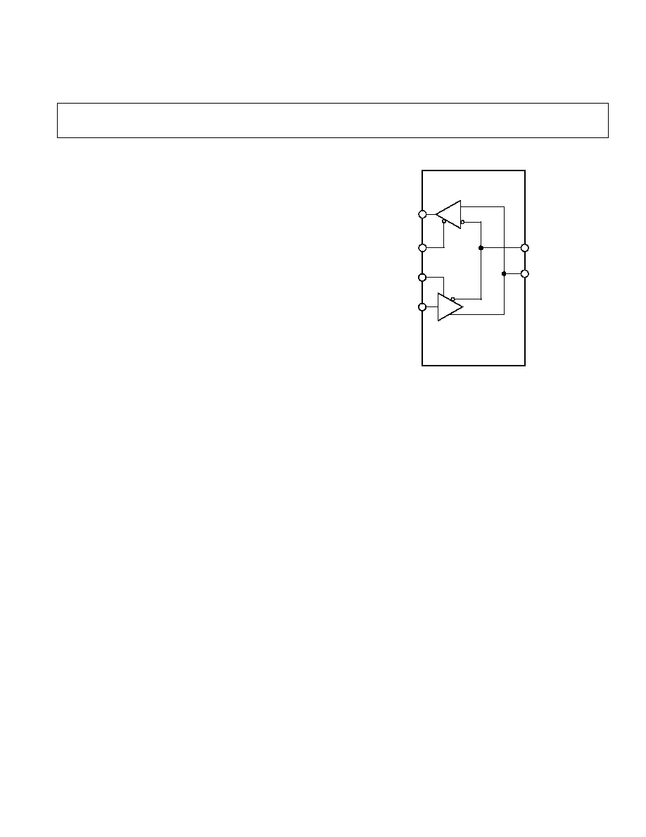
FUNCTIONAL BLOCK DIAGRAM
ADM3485E
RO
RE
DE
DI
B
A
R
D
FEATURES
Operates with +3.3 V Supply
ESD Protection: 8 kV Meets IEC1000-4-2
EFT Protection: 2 kV Meets IEC1000-4-4
EIA RS-422 and RS-485 Compliant Over Full CM Range
19 k Input Impedance
Up to 50 Transceivers on Bus
20 Mbps Data Rate
Short Circuit Protection
Specified Over Full Temperature Range
Thermal Shutdown
Interoperable with 5 V Logic
1 mA Supply Current
2 nA Shutdown Current
8 ns Skew
APPLICATIONS
Telecommunications
DTE-DCE Interface
Packet Switching
Local Area Networks
Data Concentration
Data Multiplexers
Integrated Services Digital Network (ISDN)
AppleTalk
Industrial Controls
GENERAL DESCRIPTION
The ADM3485E is a low power differential line transceiver
designed to operate using a single +3.3 V power supply. Low
power consumption makes it ideal for power sensitive applica-
tions. It is suitable for communication on multipoint bus trans-
mission lines. Internal protection against electrostatic discharge
(ESD) and electrical fast transient (EFT) allows operation in
electrically harsh environments.
It is intended for balanced data transmission and complies with
both EIA Standards RS-485 and RS-422. It contains a differen-
tial line driver and a differential line receiver, and is suitable for
half duplex data transfer.
The input impedance is 19 k
allowing up to 50 transceivers to
be connected on the bus.
Excessive power dissipation caused by bus contention or by
output shorting is prevented by a thermal shutdown circuit.
This feature forces the driver output into a high impedance
state if, during fault conditions, a significant temperature
increase is detected in the internal driver circuitry.
The receiver contains a fail-safe feature that results in a
logic high output state if the inputs are unconnected
(floating).
The ADM3485E is fabricated on BiCMOS, an advanced
mixed technology process combining low power CMOS
with fast switching bipolar technology.
The ADM3485E is fully specified over the industrial tem-
perature range and is available in 8-lead DIP and SOIC
packages.

2
REV. A
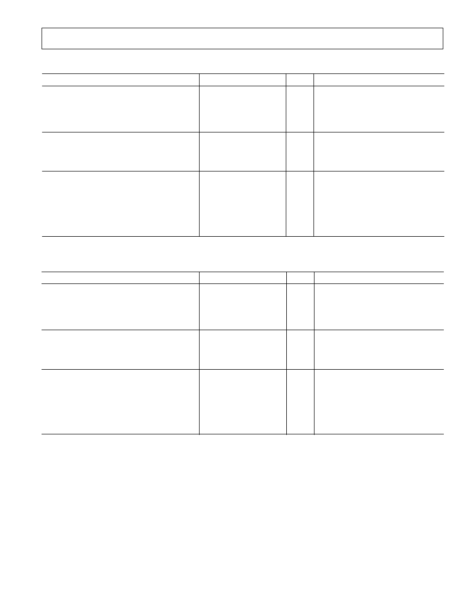
ADM3485ESPECIFICATIONS
(V
CC
= +3.3 V
0.3 V. All specifications T
MIN
to T
MAX
unless otherwise noted.)
Parameter
Min
Typ
Max
Units
Test Conditions/Comments
DRIVER
Differential Output Voltage, V
OD
2.0
V
R
L
= 100
, Figure 1, V
CC
> 3.1 V
1.5
V
R
L
= 54
, Figure 1
1.5
V
R
L
= 60
, Figure 2, 7 V < V
TST
< +12 V
|V
OD
| for Complementary Output States
0.2
V
R = 54
or 100 , Figure 1
Common-Mode Output Voltage V
OC
3
V
R = 54
or 100 , Figure 1
|V
OC
| for Complementary Output States
0.2
V
R = 54
or 100 , Figure 1
CMOS Input Logic Threshold Low, V
INL
0.8
V
CMOS Input Logic Threshold High, V
INH
2.0
V
Logic Input Current (DE, DI,
RE)
±1.0
µA
Output Short Circuit Current
±250
mA
V
O
= 7 V or +12 V
RECEIVER
Differential Input Threshold Voltage, V
TH
0.2
+0.2
V
7 V < V
CM
< +12 V
Input Voltage Hysteresis,
V
TH
50
mV
V
CM
= 0 V
Input Resistance
12
19
k
7 V < V
CM
< +12 V
Input Current (A, B)
+1
mA
V
IN
= +12 V
0.8
mA
V
IN
= 7 V
Logic Enable Input Current (
RE)
±1
µA
Output Voltage Low, V
OL
0.4
V
I
OUT
= +2.5 mA
Output Voltage High, V
OH
V
CC
0.4 V
V
I
OUT
= 1.5 mA
Short Circuit Output Current
±60
mA
V
OUT
= GND or V
CC
Three-State Output Leakage Current
±1.0
µA
V
CC
= 3.6 V, 0 V < V
OUT
< V
CC
POWER SUPPLY CURRENT
I
CC
Outputs Unloaded,
1
1.2
mA
DE = V
CC
,
RE = 0 V
1
1.2
mA
DE = 0 V,
RE = 0 V
Supply Current in Shutdown
0.002 1
µA
DE = 0 V,
RE = V
CC
ESD/EFT IMMUNITY
ESD Protection
±8
kV
IEC1000-4-2 A, B Pins Contact Discharge
EFT Protection
±2
kV
IEC1000-4-4, A, B Pins
Specifications subject to change without notice.
ADM3485E
3
REV. A
TIMING SPECIFICATIONS
Parameter
Min
Typ
Max
Units
Test Conditions/ Comments
DRIVER
Differential Output Delay T
DD
1
35
ns
R
L
= 60
, C
L1
= C
L2
= 15 pF, Figure 3
Differential Output Transition Time
1
8
15
ns
R
L
= 60
, C
L1
= C
L2
= 15 pF, Figure 3
Propagation Delay Input to Output T
PLH
, T
PHL
7
22
35
ns
R
L
= 27
, C
L1
= C
L2
= 15 pF, Figure 7
Driver O/P to O/P T
SKEW
8
ns
R
L
= 54
, C
L1
= C
L2
= 15 pF, Figure 3
ENABLE/DISABLE
Driver Enable to Output Valid
45
90
ns
R
L
= 110
, C
L
= 50 pF, Figure 2
Driver Disable Timing
40
80
ns
R
L
= 110
, C
L
= 50 pF, Figure 2
Driver Enable from Shutdown
650
110
ns
R
L
= 110
, C
L
= 15 pF, Figure 2
RECEIVER
Time to Shutdown
80
190
300
ns
Propagation Delay Input to Output T
PLH
, T
PHL
25
65
90
ns
C
L
= 15 pF, Figure 8
Skew T
PLH
T
PHL
10
ns
C
L
= 15 pF, Figure 8
Receiver Enable T
EN
25
50
ns
C
L
= 15 pF, Figure 6
Receiver Disable T
DEN
25
45
ns
C
L
= 15 pF, Figure 6
Receiver Enable from Shutdown
500
ns
C
L
= 15 pF, Figure 6
Specifications subject to change without notice.
(V
CC
= +3.3 V, T
A
= +25 C)
TIMING SPECIFICATIONS
Parameter
Min
Typ
Max
Units
Test Conditions/ Comments
DRIVER
Differential Output Delay T
DD
1
70
ns
R
L
= 60
, C
L1
= C
L2
= 15 pF, Figure 3
Differential Output Transition Time
2
8
15
ns
R
L
= 60
, C
L1
= C
L2
= 15 pF, Figure 3
Propagation Delay Input to Output T
PLH
, T
PHL
7
22
70
ns
R
L
= 27
, C
L1
= C
L2
= 15 pF, Figure 7
Driver O/P to O/P T
SKEW
10
ns
R
L
= 54
, C
L1
= C
L2
= 15 pF, Figure 3
ENABLE/DISABLE
Driver Enable to Output Valid
45
110
ns
R
L
= 110
, C
L
= 50 pF, Figure 2
Driver Disable Timing
40
110
ns
R
L
= 110
, C
L
= 50 pF, Figure 2
Driver Enable from Shutdown
650
110
ns
R
L
= 110
, C
L
= 15 pF, Figure 2
RECEIVER
Time to Shutdown
50
190
500
ns
Propagation Delay Input to Output T
PLH
, T
PHL
25
65
115
ns
C
L
= 15 pF, Figure 8
Skew T
PLH
T
PHL
20
ns
C
L
= 15 pF, Figure 8
Receiver Enable T
EN
25
50
ns
C
L
= 15 pF, Figure 6
Receiver Disable T
DEN
25
50
ns
C
L
= 15 pF, Figure 6
Receiver Enable from Shutdown
600
ns
C
L
= 15 pF, Figure 6
Specifications subject to change without notice.
(V
CC
= +3.3 V 0.3 V, T
A
= T
MIN
to T
MAX
)
ADM3485E
4
REV. A
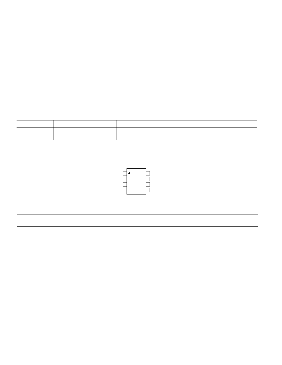
ORDERING GUIDE
Model
Temperature Range
Package Description
Package Options
ADM3485EAN
40
°C to +85°C
Plastic DIP
N-8
ADM3485EAR
40
°C to +85°C
Small Outline (SOIC)
SO-8
ABSOLUTE MAXIMUM RATINGS*
(T
A
= +25
°C unless otherwise noted)
V
CC
. . . . . . . . . . . . . . . . . . . . . . . . . . . . . . . . . . . . . . . . . +7 V
Inputs
Driver Input (DI) . . . . . . . . . . . . . . . . 0.3 V to V
CC
+ 0.3 V
Control Inputs (DE,
RE) . . . . . . . . . . 0.3 V to V
CC
+ 0.3 V
Receiver Inputs (A, B) . . . . . . . . . . . . . . . 7.5 V to +12.5 V
Outputs
Driver Outputs . . . . . . . . . . . . . . . . . . . . . 7.5 V to +12.5 V
Receiver Output . . . . . . . . . . . . . . . . . 0.5 V to V
CC
+ 0.5 V
Power Dissipation 8-Lead DIP . . . . . . . . . . . . . . . . . 800 mW
JA
, Thermal Impedance . . . . . . . . . . . . . . . . . . . . 140
°C/W
Power Dissipation 8-Lead SOIC . . . . . . . . . . . . . . . . 650 mW
JA
, Thermal Impedance . . . . . . . . . . . . . . . . . . . . 115
°C/W
Operating Temperature Range
Industrial (A Version) . . . . . . . . . . . . . . . . 40
°C to +85°C
Storage Temperature Range . . . . . . . . . . . . 65
°C to +150°C
Lead Temperature (Soldering, 10 sec) . . . . . . . . . . . . +300
°C
Vapor Phase (60 sec) . . . . . . . . . . . . . . . . . . . . . . . . +215
°C
Infrared (15 sec) . . . . . . . . . . . . . . . . . . . . . . . . . . . +220
°C
ESD Rating: Air (Human Body Model, All Pins) . . . . . >4 kV
ESD Rating: IEC1000-4-2 Contact (A, B Pins) . . . . . . >8 kV
EFT Rating: IEC1000-4-4 (A, B Pins) . . . . . . . . . . . . . >2 kV
*Stresses above those listed under Absolute Maximum Ratings may cause perma-
nent damage to the device. This is a stress rating only; functional operation of the
device at these or any other conditions above those listed in the operational sections
of this specification is not implied. Exposure to absolute maximum ratings for
extended periods of time may affect device reliability.
PIN CONFIGURATION
DIP/SOIC
TOP VIEW
(Not to Scale)
8
7
6
5
1
2
3
4
RO
RE
DE
DI
V
CC
B
A
GND
ADM3485E
PIN FUNCTION DESCRIPTIONS
Mnemonic
DIP/
Pin
SOIC
Function
RO
1
Receiver Output. High when A > B by 200 mV or low when A < B by 200 mV.
RE
2
Receiver Output Enable. With
RE low, the receiver output RO is enabled. With RE high, the output goes
high impedance. If
RE is high and DE low, the ADM3485E enters a shutdown state.
DE
3
Driver Output Enable. A high level enables the driver differential outputs, A and B. A low level places it in a
high impedance state.
DI
4
Driver Input. When the driver is enabled, a logic low on DI forces A low and B high, while a logic high on DI
forces A high and B low.
GND
5
Ground Connection, 0 V.
A
6
Noninverting Receiver Input A/Driver Output A.
B
7
Inverting Receiver Input B/Driver Output B.
V
CC
8
Power Supply, 3.3 V
± 0.3 V.
ADM3485E
5
REV. A
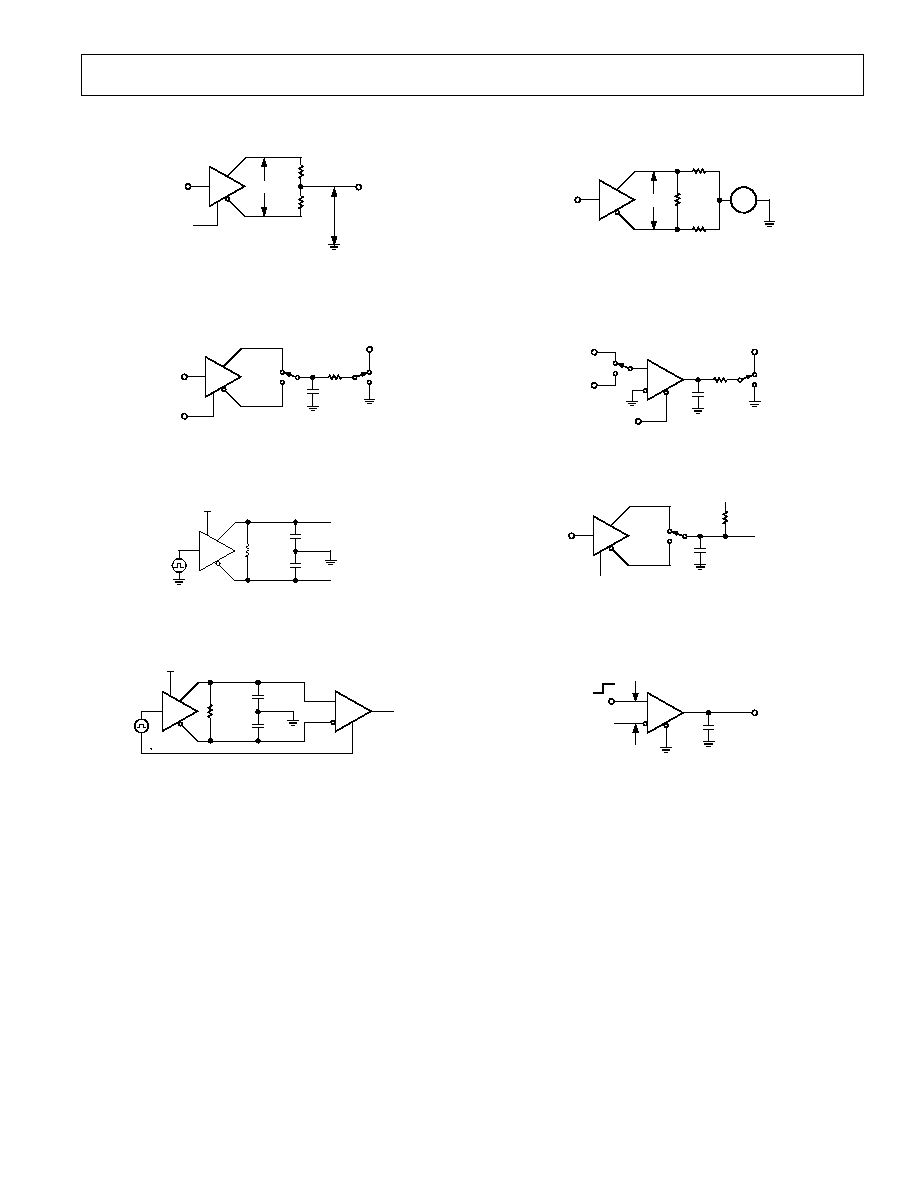
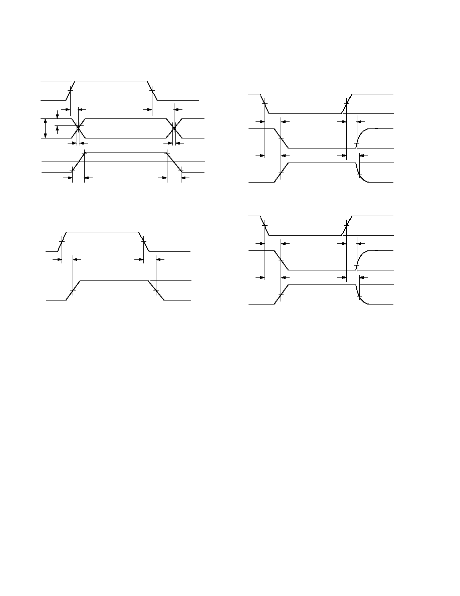
Test Circuits
V
OD
R/2
R/2
V
OC
V
CC
Figure 1. Driver Voltage Measurement Test Circuit
S1
C
L
V
OUT
V
CC
DE
R
L
S2
0V OR 3V
DE IN
Figure 2. Driver Enable/Disable Test Circuit
V
OUT
D
C
L1
DI
RL
DIFF
C
L2
Figure 3. Driver Differential Output Delay Test Circuit
D
C
L1
DI
RL
DIFF
C
L2
R
RE
RO
A
B
Figure 4. Driver/Receiver Propagation Delay Test Circuit
V
OD3
R
L
375
375
V
TST
Figure 5. Driver Voltage Measurement Test Circuit 2
S1
C
L
V
OUT
V
CC
RE
R
L
S2
RE IN
+1.5V
1.5V
Figure 6. Receiver Enable/Disable Test Circuit
S1
C
L
V
CC
DE
R
L
IN
V
OUT
V
OM
Figure 7. Driver Propagation Delay Test Circuit
C
L
V
OUT
RE
V
ID
+1.5V
0V
3V
Figure 8. Receiver Propagation Delay Test Circuit
ADM3485E
6
REV. A
3V
0V
B
A
VO
1/2 VO
t
SKEW
t
SKEW
1.5V
1.5V
t
PLH
t
PLH
VO
90% POINT
10% POINT
0V
VO
t
R
90% POINT
10% POINT
t
F
Figure 9. Driver Propagation Delay, Rise/Fall Timing
0V
1.5V
t
PLH
0V
1.5V
t
PLH
AB
RO
V
OH
V
OL
Figure 10. Receiver Propagation Delay
Switching Characteristics
1.5V
1.5V
t
ZL
0V
V
OH
V
OL
1.5V
t
LZ
O/P
LOW
1.5V
t
ZH
O/P
HIGH
t
HZ
V
OH
0.25V
V
OL
+ 0.25V
3V
DE
D
D
0V
Figure 11. Driver Enable/Disable Timing
1.5V
1.5V
t
ZL
0V
V
OH
V
OL
1.5V
t
LZ
O/P
LOW
1.5V
t
ZH
O/P
HIGH
t
HZ
V
OH
0.25V
V
OL
+ 0.25V
3V
RE
R
R
0V
Figure 12. Receiver Enable/Disable Timing
OUTPUT LOW VOLTAGE V
14
0
0
3.5
0.5
OUTPUT CURRENT
mA
1.0
1.5
2.0
2.5
3.0
12
8
6
4
2
10
Figure 13. Output Current vs. Receiver Output Low
Voltage
TEMPERATURE C
0.8
0.1
50
90
30
RECEIVER OUTPUT LOW VOLTAGE
V
10
10
30
50
70
0.7
0.5
0.4
0.3
0.2
0.6
110
Figure 14. Receiver Output Low Voltage vs. Temperature
DIFFERENTIAL OUTPUT VOLTAGE V
120
0
3.0
0.5
DRIVER OUTPUT CURRENT
mA
1.0
1.5
2.0
2.5
100
60
40
20
0
80
Figure 15. Driver Output Current vs. Differential
Output Voltage
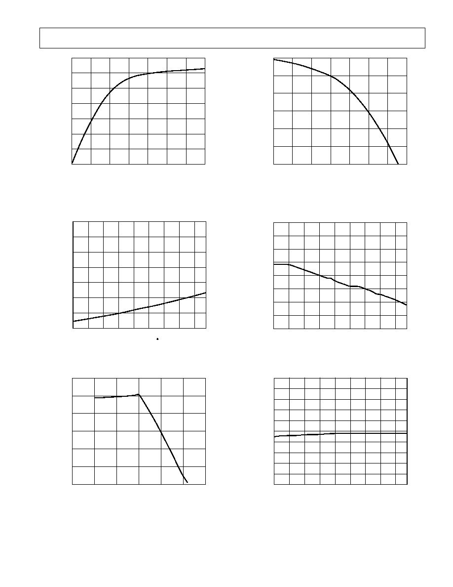
Typical Performance CharacteristicsADM3485E
7
OUTPUT HIGH VOLTAGE V
12
0
3.0
0.5
OUTPUT CURRENT
mA
1.0
1.5
2.0
2.5
10
6
4
2
0
8
3.5
Figure 16. Output Current vs. Receiver Output High
Voltage
TEMPERATURE C
3.30
50
70
30
RECEIVER O/P HIGH VOLTAGE
V
10
10
30
50
3.25
3.15
3.10
3.05
2.90
3.20
3.00
2.95
90
110
Figure 17. Receiver Output High Voltage vs. Temperature
TEMPERATURE C
2.6
50
70
30
V
OD
V
10
10
30
50
2.5
2.3
2.2
2.1
1.8
2.4
2.0
1.9
90
110
1.7
1.6
Figure 18. Driver Differential Output Voltage vs. Temperature
REV. A
ADM3485E
8
REV. A
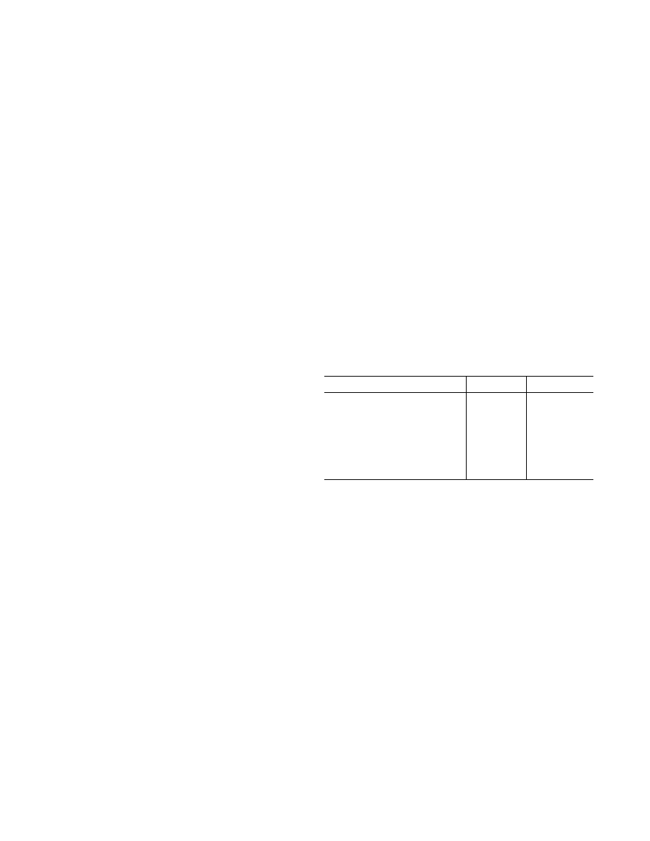
Table I. Comparison of RS-422 and RS-485 Interface Standards
Specification
RS-422
RS-485
Transmission Type
Differential
Differential
Maximum Data Rate
10 MB/s
10 MB/s
Maximum Cable Length
4000 ft.
4000 ft.
Minimum Driver Output Voltage
±2 V
±1.5 V
Driver Load Impedance
100
54
Receiver Input Resistance
4 k
min
12 k
min
Receiver Input Sensitivity
±200 mV
±200 mV
Receiver Input Voltage Range
7 V to +7 V 7 V to +12 V
No. of Drivers/Receivers Per Line
1/10
32/32
Table II. Transmitting Truth Table
Transmitting
Inputs
Outputs
RE
DE
DI
B
A
X
1
1
0
1
X
1
0
1
0
0
0
X
Hi-Z
Hi-Z
1
0
X
Hi-Z
Hi-Z
Table III. Receiving Truth Table
Receiving
Inputs
Outputs
RE
DE
AB
RO
0
X
> +0.2 V
1
0
X
< 0.2 V
0
0
X
Inputs O/C
1
1
X
X
Hi-Z
ESD/EFT TRANSIENT PROTECTION SCHEME
The ADM3485E uses protective clamping structures on its
inputs and outputs that clamp the voltage to a safe level and
dissipate the energy present in ESD (Electrostatic) and EFT
(Electrical Fast Transients) discharges.
The protection structure achieves ESD protection up to
±8 kV
according to IEC1000-4-2, and EFT protection up to
±2 kV on
all I-O lines.
ESD TESTING
Two coupling methods are used for ESD testing, contact dis-
charge and air-gap discharge. Contact discharge calls for a di-
rect connection to the unit being tested. Air-gap discharge uses
a higher test voltage but does not make direct contact with the
unit under test. With air discharge, the discharge gun is moved
toward the unit under test, developing an arc across the air gap,
hence the term air-discharge. This method is influenced by hu-
midity, temperature, barometric pressure, distance and rate of
closure of the discharge gun. The contact-discharge method,
while less realistic, is more repeatable and is gaining acceptance
and preference over the air-gap method.
Although very little energy is contained within an ESD pulse,
the extremely fast rise time, coupled with high voltages, can
cause failures in unprotected semiconductors. Catastrophic
destruction can occur immediately as a result of arcing or heat-
ing. Even if catastrophic failure does not occur immediately, the
device may suffer from parametric degradation, which may
result in degraded performance. The cumulative effects of con-
tinuous exposure can eventually lead to complete failure.
I-O lines are particularly vulnerable to ESD damage. Simply
touching or plugging in an I-O cable can result in a static dis-
charge that can damage or completely destroy the interface
product connected to the I-O port.
It is extremely important, therefore, to have high levels of ESD
protection on the I-O lines.
It is possible that the ESD discharge could induce latchup in the
device under test, so it is important that ESD testing on the I-O
pins be carried out while device power is applied. This type of
testing is more representative of a real-world I-O discharge
where the equipment is operating normally when the discharge
occurs.
TEMPERATURE C
1.20
50
70
30
I
CC
mA
10
10
30
50
1.15
1.05
1.00
0.95
0.80
1.10
0.90
0.85
90
110
0.75
0.70
I
CC
(mA)
RE = LO, DE = LO
I
CC
(mA) DE = V
CC
,
RE = X
Figure 19. Supply Current vs. Temperature
TEMPERATURE C
100
40
80
20
I
CC
nA
0
20
40
60
90
70
60
50
20
80
40
30
10
0
I
CC
(mA)
Figure 20. Shutdown Current vs. Temperature
ADM3485E
9
REV. A
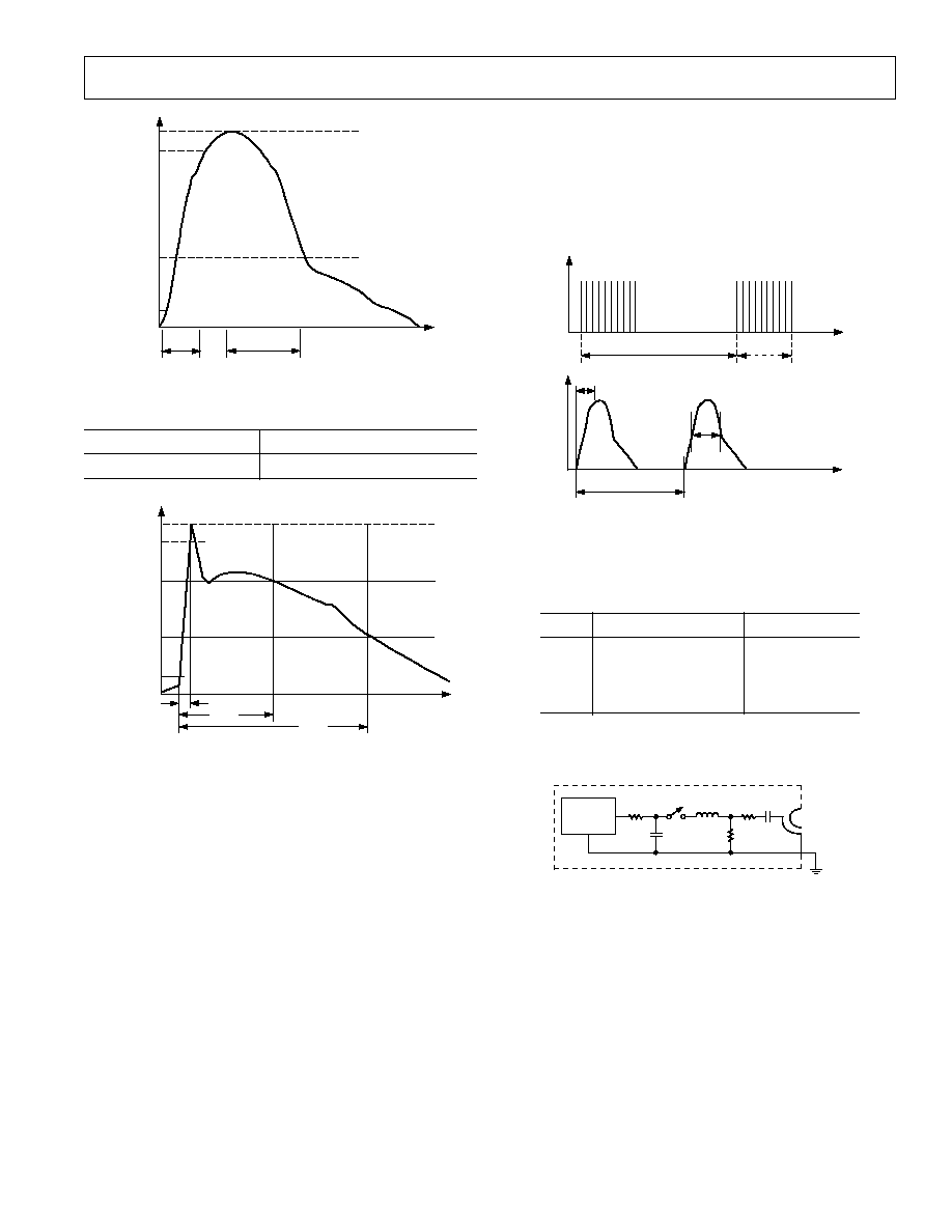
100%
90%
36.8%
10%
t
RL
t
DL
I
PEAK
TIME
t
Figure 21. Human Body Model Current Waveform
Table IV. ESD Test Results
ESD Test Method
I-O Pins
IEC1000-4-2: Contact
±8 kV
TIME
t
100%
90%
10%
I
PEAK
0.1 TO 1ns
30ns
60ns
Figure 22. IEC1000-4-2 ESD Current Waveform
FAST TRANSIENT BURST IMMUNITY (IEC1000-4-4)
IEC1000-4-4 (previously 801-4) covers electrical fast-transient/
burst (EFT) immunity. Electrical fast transients occur as a
result of arcing contacts in switches and relays. The tests simu-
late the interference generated when, for example, a power relay
disconnects an inductive load. A spark is generated due to the
well known back EMF effect. In fact, the spark consists of a
burst of sparks as the relay contacts separate. The voltage ap-
pearing on the line, therefore, consists of a burst of extremely
fast transient impulses. A similar effect occurs when switching
on fluorescent lights.
The fast transient burst test, defined in IEC1000-4-4, simulates
this arcing and its waveform is illustrated in Figure 23. It con-
sists of a burst of 2.5 kHz to 5 kHz transients repeating at
300 ms intervals. It is specified for both power and data lines.
Four severity levels are defined in terms of an open-circuit volt-
age as a function of installation environment. The installation
environments are defined as
1. Well-Protected
2. Protected
3. Typical Industrial
4. Severe Industrial
300ms
16ms
5ns
50ns
0.2/0.4ms
t
t
V
V
Figure 23. IEC1000-4-4 Fast Transient Waveform
Table V shows the peak voltages for each of the environments.
Table V. Peak Voltages
Level
V
PEAK
(kV) PSU
V
PEAK
(kV) I-O
1
0.5
0.25
2
1
0.5
3
2
1
4
4
2
A simplified circuit diagram of the actual EFT generator is
illustrated in Figure 24.
HIGH
VOLTAGE
SOURCE
R
C
C
C
L
Z
S
R
M
C
D
50
OUTPUT
Figure 24. EFT Generator
These transients are coupled onto the signal lines using an EFT
coupling clamp. The clamp is 1 m long and completely sur-
rounds the cable, providing maximum coupling capacitance
(50 pF to 200 pF typ) between the clamp and the cable. High
energy transients are capacitively coupled onto the signal lines.
Fast rise times (5 ns) as specified by the standard result in very
effective coupling. This test is very severe since high voltages are
coupled onto the signal lines. The repetitive transients can often
cause problems, where single pulses do not. Destructive latchup
may be induced due to the high energy content of the transients.
Note that this stress is applied while the interface products are
powered up and are transmitting data. The EFT test applies
hundreds of pulses with higher energy than ESD. Worst case
transient current on an I-O line can be as high as 40 A.
ADM3485E
10
REV. A
Test results are classified according to the following
1. Normal performance within specification limits.
2. Temporary degradation or loss of performance that is self-
recoverable.
3. Temporary degradation or loss of function or performance
that requires operator intervention or system reset.
4. Degradation or loss of function that is not recoverable due to
damage.
APPLICATIONS INFORMATION
Differential Data Transmission
Differential data transmission is used to reliably transmit data at
high rates over long distances and through noisy environments.
Differential transmission nullifies the effects of ground shifts
and noise signals that appear as common-mode voltages on the
line.
Two main standards are approved by the Electronics Industries
Association (EIA) which specify the electrical characteristics of
transceivers used in differential data transmission. The RS-422
standard specifies data rates up to 10 MBaud and line lengths
up to 4000 ft. A single driver can drive a transmission line with
up to 10 receivers.
The RS-485 standard was defined to cater to true multipoint
communications. This standard meets or exceeds all the re-
quirements of RS-422, but also allows multiple drivers and
receivers to be connected to a single bus. An extended common-
mode range of 7 V to +12 V is defined.
The most significant difference between RS-422 and RS-485 is
the fact that the drivers may be disabled thereby allowing more
than one to be connected to a single line. Only one driver should
be enabled at a time, but the RS-485 standard contains addi-
tional specifications to guarantee device safety in the event of
line contention.
Cable and Data Rate
The transmission line of choice for RS-485 communications is a
twisted pair. Twisted pair cable tends to cancel common-mode
noise and also causes cancellation of the magnetic fields gener-
ated by the current flowing through each wire, thereby reducing
the effective inductance of the pair.
The ADM3485E is designed for bidirectional data communica-
tions on multipoint transmission lines. A typical application
showing a multipoint transmission network is illustrated in
Figure 23. Only one driver can transmit at a particular time, but
multiple receivers may be enabled simultaneously.
As with any transmission line, it is important that reflections are
minimized. This may be achieved by terminating the extreme
ends of the line using resistors equal to the characteristic imped-
ance of the line. Stub lengths of the main line should also be
kept as short as possible. A properly terminated transmission
line appears purely resistive to the driver.
Receiver Open-Circuit Fail-Safe
The receiver input includes a fail-safe feature that guarantees a
logic high on the receiver when the inputs are open circuit or
floating.
Table VI. Comparison of RS-422 and RS-485 Interface
Standards
Specification
RS-422
RS-485
Transmission Type
Differential
Differential
Maximum Cable Length
4000 ft.
4000 ft.
Minimum Driver Output Voltage
±2 V
±1.5 V
Driver Load Impedance
100
54
Receiver Input Resistance
4 k
min
12 k
min
Receiver Input Sensitivity
±200 mV
±200 mV
Receiver Input Voltage Range
7 V to +7 V 7 V to +12 V
ADM3485E
11
REV. A
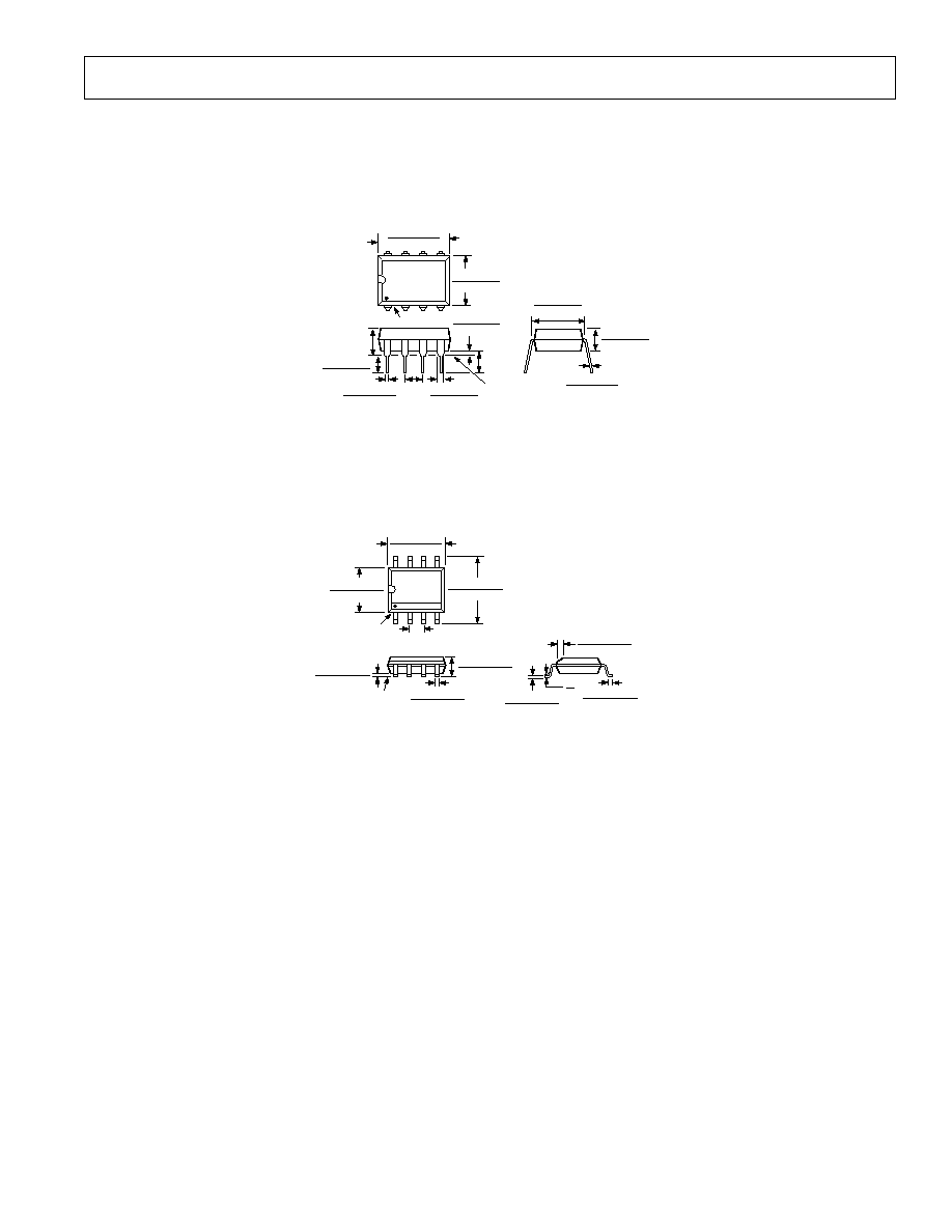
OUTLINE DIMENSIONS
Dimensions shown in inches and (mm).
8-Lead Plastic DIP
(N-8)
8
1
4
5
0.430 (10.92)
0.348 (8.84)
0.280 (7.11)
0.240 (6.10)
PIN 1
SEATING
PLANE
0.022 (0.558)
0.014 (0.356)
0.060 (1.52)
0.015 (0.38)
0.210 (5.33)
MAX
0.130
(3.30)
MIN
0.070 (1.77)
0.045 (1.15)
0.100
(2.54)
BSC
0.160 (4.06)
0.115 (2.93)
0.325 (8.25)
0.300 (7.62)
0.015 (0.381)
0.008 (0.204)
0.195 (4.95)
0.115 (2.93)
8-Lead SOIC
(SO-8)
0.0098 (0.25)
0.0075 (0.19)
0.0500 (1.27)
0.0160 (0.41)
8
0
0.0196 (0.50)
0.0099 (0.25)
45
8
5
4
1
0.1968 (5.00)
0.1890 (4.80)
0.2440 (6.20)
0.2284 (5.80)
PIN 1
0.1574 (4.00)
0.1497 (3.80)
0.0500 (1.27)
BSC
0.0688 (1.75)
0.0532 (1.35)
SEATING
PLANE
0.0098 (0.25)
0.0040 (0.10)
0.0192 (0.49)
0.0138 (0.35)
C333805/00 (rev. A) 00075
PRINTED
IN
U.S.A.