 | ÐлекÑÑоннÑй компоненÑ: ADM3491AR | СкаÑаÑÑ:  PDF PDF  ZIP ZIP |
Äîêóìåíòàöèÿ è îïèñàíèÿ www.docs.chipfind.ru
REV. 0
Information furnished by Analog Devices is believed to be accurate and
reliable. However, no responsibility is assumed by Analog Devices for its
use, nor for any infringements of patents or other rights of third parties
which may result from its use. No license is granted by implication or
otherwise under any patent or patent rights of Analog Devices.
a
ADM3491
One Technology Way, P.O. Box 9106, Norwood, MA 02062-9106, U.S.A.
Tel: 781/329-4700
World Wide Web Site: http://www.analog.com
Fax: 781/326-8703
© Analog Devices, Inc., 1998
3.3 V, Full Duplex, 840 A
20 Mbps, EIA RS-485 Transceiver
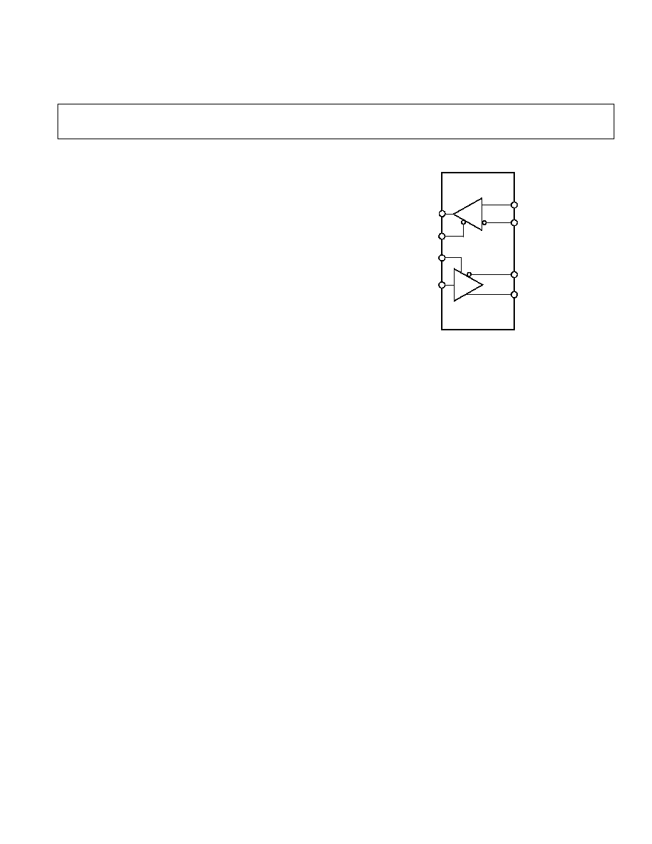
FUNCTIONAL BLOCK DIAGRAM
R
D
RE
DE
DI
A
B
Z
Y
ADM3491
RO
FEATURES
Operates with +3.3 V Supply
EIA RS-422 and RS-485 Compliant Over Full CM Range
19 k Input Impedance
Up to 50 Transceivers on Bus
20 Mbps Data Rate
Short Circuit Protection
Specified Over Full Temperature Range
Thermal Shutdown
Interoperable with 5 V Logic
840 A Supply Current
2 nA Shutdown Current
Also Available in TSSOP Package
Meets IEC1000-4-4 (>1 kV)
8 ns Skew
Upgrade for MAX 3491, SN75ALS180
APPLICATIONS
Telecommunications
DTE-DCE Interface
Packet Switching
Local Area Networks
Data Concentration
Data Multiplexers
Integrated Services Digital Network (ISDN)
AppleTalk
Industrial Controls
GENERAL DESCRIPTION
The ADM3491 is a low power differential line transceiver
designed to operate using a single +3.3 V power supply. Low
power consumption coupled with a shutdown mode make it
ideal for power sensitive applications. It is suitable for commu-
nication on multipoint bus transmission lines.
It is intended for balanced data transmission and complies with
both EIA Standards RS-485 and RS-422. It contains a differen-
tial line driver and a differential line receiver, making it suitable
for full duplex data transfer.
The input impedance is 19 k
allowing up to 50 transceivers to
be connected on the bus.
Excessive power dissipation caused by bus contention or by
output shorting is prevented by a thermal shutdown circuit.
This feature forces the driver output into a high impedance state
if, during fault conditions, a significant temperature increase is
detected in the internal driver circuitry.
The receiver contains a fail-safe feature that results in a
logic high output state if the inputs are unconnected
(floating).
The ADM3491 is fabricated on BiCMOS, an advanced
mixed technology process combining low power CMOS
with fast switching bipolar technology.
The ADM3491 is fully specified over the industrial tem-
perature range and is available in DIP and SOIC packages
as well as a new space saving TSSOP package.

2
REV. 0
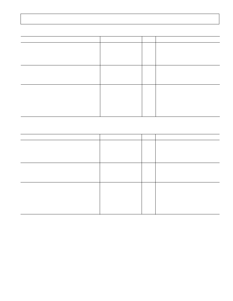
ADM3491SPECIFICATIONS
(V
CC
= +3.3 V 0.3 V. All specifications T
MIN
to T
MAX
unless otherwise noted.)
Parameter
Min
Typ
Max
Units
Test Conditions/Comments
DRIVER
Differential Output Voltage, V
OD
2.0
V
R
L
= 100
, Figure 1, V
CC
> 3.1 V
1.5
V
R
L
= 54
, Figure 1
1.5
V
R
L
= 60
, Figure 2, 7 V < V
TST
< +12 V
|V
OD
| for Complementary Output States
0.2
V
R = 54
or 100
, Figure 1
Common-Mode Output Voltage V
OC
3
V
R = 54
or 100
, Figure 1
|V
OC
| for Complementary Output States
0.2
V
R = 54
or 100
, Figure 1
CMOS Input Logic Threshold Low, V
INL
0.8
V
CMOS Input Logic Threshold High, V
INH
2.0
V
Logic Input Current (DE, DI, RE)
±
1.0
µ
A
Output Leakage (Y, Z) Current
±
3
µ
A
V
O
= 7 V or +12 V, V
CC
= 0 V or 3.6 V
Output Short Circuit Current
±
250
mA
V
O
= 7 V or +12 V
RECEIVER
Differential Input Threshold Voltage, V
TH
0.2
+0.2
V
7 V < V
CM
< +12 V
Input Voltage Hysteresis,
V
TH
50
mV
V
CM
= 0 V
Input Resistance
12
19
k
7 V < V
CM
< +12 V
Input Current (A, B)
+1
mA
V
IN
= +12 V
0.8
mA
V
IN
= 7 V
Logic Enable Input Current (
RE)
±
1
µ
A
Output Voltage Low, V
OL
0.4
V
I
OUT
= +2.5 mA
Output Voltage High, V
OH
V
CC
0.4 V
V
I
OUT
= 1.5 mA
Short Circuit Output Current
±
60
mA
V
OUT
= GND or V
CC
Three-State Output Leakage Current
±
1.0
µ
A
V
CC
= 3.6 V, 0 V < V
OUT
< V
CC
POWER SUPPLY CURRENT
I
CC
Outputs Unloaded,
0.84
1.2
mA
DE = V
CC
,
RE = 0 V
0.84
1.2
mA
DE = 0 V,
RE = 0 V
Supply Current in Shutdown
0.002
1
µ
A
DE = 0 V,
RE = V
CC
Specifications subject to change without notice.
ADM3491
3
REV. 0
TIMING SPECIFICATIONS
Parameter
Min
Typ
Max
Units
Test Conditions/ Comments
DRIVER
Differential Output Delay T
DD
1
35
ns
R
L
= 60
, C
L1
= C
L2
= 15 pF, Figure 5
Differential Output Transition Time
1
8
15
ns
R
L
= 60
, C
L1
= C
L2
= 15 pF, Figure 5
Propagation Delay Input to Output T
PLH
, T
PHL
7
22
35
ns
R
L
= 27
, C
L1
= C
L2
= 15 pF, Figure 6
Driver O/P to O/P T
SKEW
8
ns
R
L
= 54
, C
L1
= C
L2
= 15 pF, Figure 6
ENABLE/DISABLE
Driver Enable to Output Valid
45
90
ns
R
L
= 110
, C
L
= 50 pF, Figure 3
Driver Disable Timing
40
80
ns
R
L
= 110
, C
L
= 50 pF, Figure 3
Driver Enable from Shutdown
650
110
ns
R
L
= 110
, C
L
= 15 pF, Figure 3
RECEIVER
Time to Shutdown
80
190
300
ns
Propagation Delay Input to Output T
PLH
, T
PHL
25
65
90
ns
C
L
= 15 pF, Figure 8
Skew T
PLH
T
PHL
10
ns
C
L
= 15 pF, Figure 8
Receiver Enable T
EN
25
50
ns
C
L
= 15 pF, Figure 4
Receiver Disable T
DEN
25
45
ns
C
L
= 15 pF, Figure 4
Receiver Enable from Shutdown
500
ns
C
L
= 15 pF, Figure 4
(V
CC
= +3.3 V, T
A
= +25 C)
TIMING SPECIFICATIONS
Parameter
Min
Typ
Max
Units
Test Conditions/ Comments
DRIVER
Differential Output Delay T
DD
1
70
ns
R
L
= 60
, C
L1
= C
L2
= 15 pF, Figure 5
Differential Output Transition Time
2
8
15
ns
R
L
= 60
, C
L1
= C
L2
= 15 pF, Figure 5
Propagation Delay Input to Output T
PLH
, T
PHL
7
22
70
ns
R
L
= 27
, C
L1
= C
L2
= 15 pF, Figure 6
Driver O/P to O/P T
SKEW
10
ns
R
L
= 54
, C
L1
= C
L2
= 15 pF, Figure 6
ENABLE/DISABLE
Driver Enable to Output Valid
45
110
ns
R
L
= 110
, C
L
= 50 pF, Figure 3
Driver Disable Timing
40
110
ns
R
L
= 110
, C
L
= 50 pF, Figure 3
Driver Enable from Shutdown
650
110
ns
R
L
= 110
, C
L
= 15 pF, Figure 3
RECEIVER
Time to Shutdown
50
190
500
ns
Propagation Delay Input to Output T
PLH
, T
PHL
25
65
115
ns
C
L
= 15 pF, Figure 8
Skew T
PLH
T
PHL
20
ns
C
L
= 15 pF, Figure 8
Receiver Enable T
EN
25
50
ns
C
L
= 15 pF, Figure 4
Receiver Disable T
DEN
25
50
ns
C
L
= 15 pF, Figure 4
Receiver Enable from Shutdown
600
ns
C
L
= 15 pF, Figure 4
(V
CC
= +3.3 V 0.3 V, T
A
= T
MIN
to T
MAX
)

ADM3491
4
REV. 0
ORDERING GUIDE
Model
Temperature Range
Package Description
Package Options
ADM3491AN
40
°
C to +85
°
C
Plastic DIP
N-14
ADM3491AR
40
°
C to +85
°
C
Small Outline (SOIC)
R-14
ADM3491ARU
40
°
C to +85
°
C
Thin Shrink Small Outline (TSSOP)
RU-16
ABSOLUTE MAXIMUM RATINGS*
(T
A
= +25
°
C unless otherwise noted)
V
CC
. . . . . . . . . . . . . . . . . . . . . . . . . . . . . . . . . . . . . . . . . +7 V
Inputs
Driver Input (DI) . . . . . . . . . . . . . . . . 0.3 V to V
CC
+ 0.3 V
Control Inputs (DE,
RE) . . . . . . . . . .0.3 V to V
CC
+ 0.3 V
Receiver Inputs (A, B) . . . . . . . . . . . . . . . 7.5 V to +12.5 V
Outputs
Driver Outputs . . . . . . . . . . . . . . . . . . . . . 7.5 V to +12.5 V
Receiver Output . . . . . . . . . . . . . . . . . 0.5 V to V
CC
+0.5 V
Power Dissipation 14-Lead DIP . . . . . . . . . . . . . . . . 800 mW
JA
, Thermal Impedance . . . . . . . . . . . . . . . . . . . 140
°
C/W
Power Dissipation 14-Lead SOIC . . . . . . . . . . . . . . . 650 mW
JA
, Thermal Impedance . . . . . . . . . . . . . . . . . . . 115
°
C/W
Power Dissipation 16-Lead TSSOP . . . . . . . . . . . . . . 500 mW
JA
, Thermal Impedance . . . . . . . . . . . . . . . . . . . 158
°
C/W
Operating Temperature Range
Industrial (A Version) . . . . . . . . . . . . . . . . 40
°
C to +85
°
C
Storage Temperature Range . . . . . . . . . . . . 65
°
C to +150
°
C
Lead Temperature (Soldering, 10 sec) . . . . . . . . . . . . +300
°
C
Vapor Phase (60 sec) . . . . . . . . . . . . . . . . . . . . . . . . +215
°
C
Infrared (15 sec) . . . . . . . . . . . . . . . . . . . . . . . . . . .+220
°
C
ESD Rating . . . . . . . . . . . . . . . . . . . . . . . . . . . . . . . . . . >2 kV
EFT Rating (IEC1000-4-4) . . . . . . . . . . . . . . . . . . . . . . >1 kV
*Stresses above those listed under Absolute Maximum Ratings may cause perma-
nent damage to the device. This is a stress rating only; functional operation of the
device at these or any other conditions above those listed in the operational
sections of this specification is not implied. Exposure to absolute maximum
ratings for extended periods of time may affect device reliability.
ADM3491
5
REV. 0
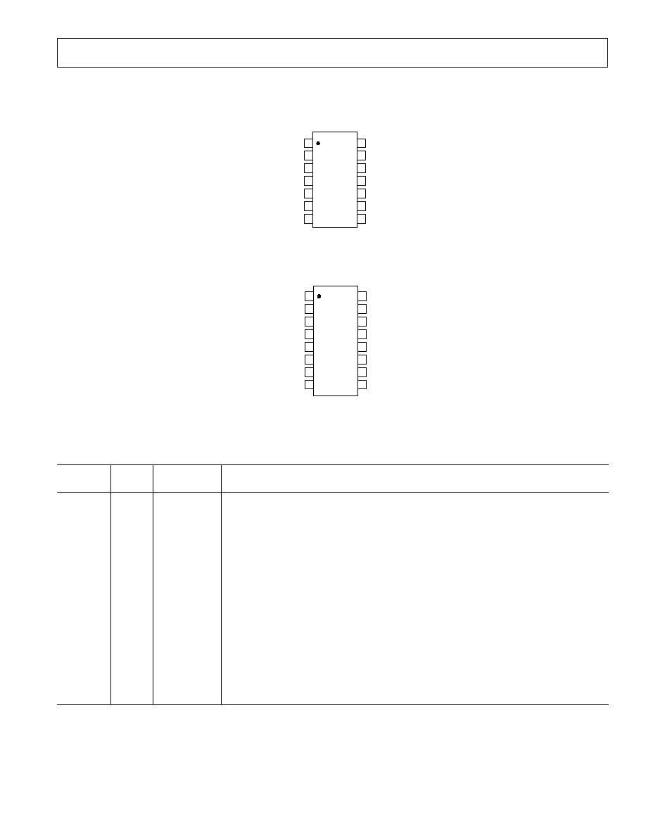
PIN CONFIGURATION
DIP/SOIC
14
13
12
11
10
9
8
1
2
3
4
5
6
7
ADM3491
NC
RO
RE
DE
DI
GND
GND
TOP VIEW
(Not to Scale)
V
CC
A
B
Z
Y
NC
V
CC
NC = NO CONNECT
TSSOP
V
CC
NC
RO
RE
DE
DI
NC
GND
NC
A
B
NC
Z
Y
NC
NC
16
15
14
13
12
11
10
9
1
2
3
4
5
6
7
8
NC = NO CONNECT
ADM3491
TOP VIEW
(Not to Scale)
PIN FUNCTION DESCRIPTIONS
Mnemonic
DIP/
Pin
SOIC
TSSOP
Function
NC
1, 8
2, 7, 9, 10,
13, 16
No Connect.
RO
2
3
Receiver Output. High when A > B by 200 mV or Low when A < B by 200 mV.
RE
3
4
Receiver Output Enable. With
RE low, the receiver output RO is enabled. With RE high,
the output goes high impedance. If
RE is high and DE low, the ADM3491 enters a
shutdown state.
DE
4
5
Driver Output Enable. A high level enables the driver differential outputs, Y and Z. A low
level places it in a high impedance state.
DI
5
6
Driver Input. When the driver is enabled, a logic Low on DI forces Y low and Z high while
a logic high on DI forces Y high and Z low.
GND
6, 7
8
Ground Connection, 0 V.
Y
9
11
Noninverting Driver Output Y.
Z
10
12
Inverting Driver Output Z.
B
11
14
Inverting Receiver Input B.
A
12
15
Noninverting Receiver Input A.
V
CC
13, 14
1
Power Supply, 3.3 V
±
0.3 V.
ADM3491
6
REV. 0
Test Circuits
V
CC
R/2
R/2
V
OC
V
OD
Figure 1. Driver Voltage Measurement Test Circuit
0V OR 3V
DE IN
DE
S1
R
L
C
L
V
OUT
V
CC
S2
Figure 2. Driver Enable/Disable Test Circuit
DI
D
RL
DIFF
C
L1
C
L2
V
OUT
Figure 3. Driver Differential Output Delay Test Circuit
DI
RL
DIFF
C
L1
C
L2
RO
RE
A
B
R
D
Figure 4. Driver/Receiver Propagation Delay Test Circuit
R
L
375
375
V
TST
V
OD3
Figure 5. Driver Voltage Measurement Test Circuit 2
+1.5V
1.5V
RE
IN
RE
C
L
S2
V
OUT
V
CC
S1
R
L
Figure 6. Receiver Enable/Disable Test Circuit
DE
S1
IN
V
CC
C
L
V
OUT
R
L
V
OM
Figure 7. Driver Propagation Delay Test Circuit
RE
0V
3V
V
ID
+1.5V
C
L
V
OUT
Figure 8. Receiver Propagation Delay Test Circuit
ADM3491
7
REV. 0
3V
0V
Z
VO
Y
VO
0V
VO
1/2VO
90% POINT
10% POINT
t
R
t
SKEW
t
F
10% POINT
90% POINT
1.5V
t
PHL
1.5V
t
PLH
t
SKEW
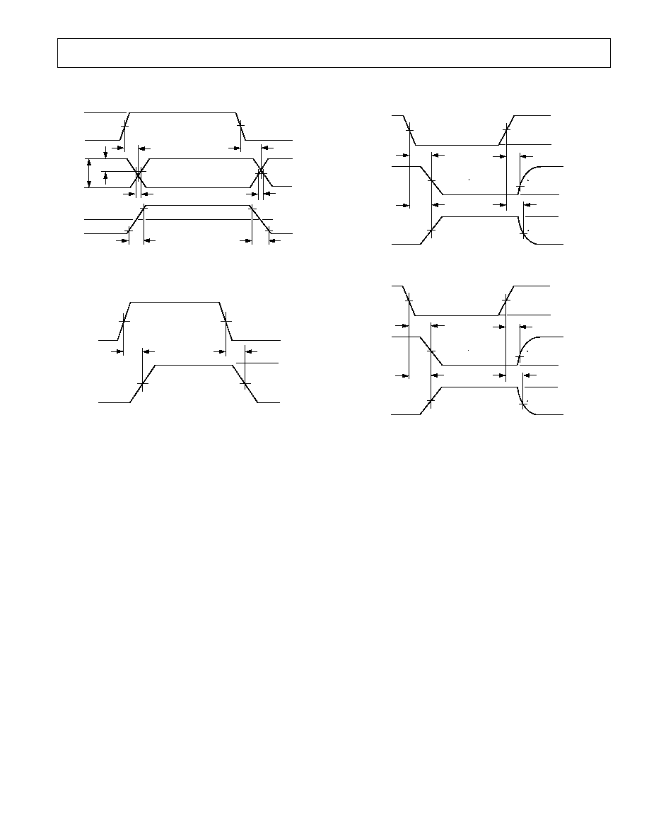
Figure 9. Driver Propagation Delay, Rise/Fall Timing
AB
RO
0V
t
PLH
1.5V
0V
V
OH
t
PHL
V
OL
1.5V
Figure 10. Receiver Propagation Delay
Switching Characteristics
RE
R
R
0V
1.5V
O/P HIGH
O/P
LOW
V
OL
+ 0.25V
t
HZ
V
OH
0.25V
V
OL
V
OH
t
ZH
t
ZL
t
LZ
1.5V
1.5V
1.5V
0V
3V
Figure 11. Driver Enable/Disable Timing
RE
R
R
0V
1.5V
O/P HIGH
O/P
LOW
V
OL
+ 0.25V
t
HZ
V
OH
0.25V
V
OL
V
OH
t
ZH
t
ZL
t
LZ
1.5V
1.5V
1.5V
0V
3V
Figure 12. Receiver Enable/Disable Timing
ADM3491
8
REV. 0
OUTPUT VOLTAGE Volts
14
0
0
3.5
0.5
1
1.5
2
2.5
3
12
8
6
4
2
10
OUTPUT CURRENT mA
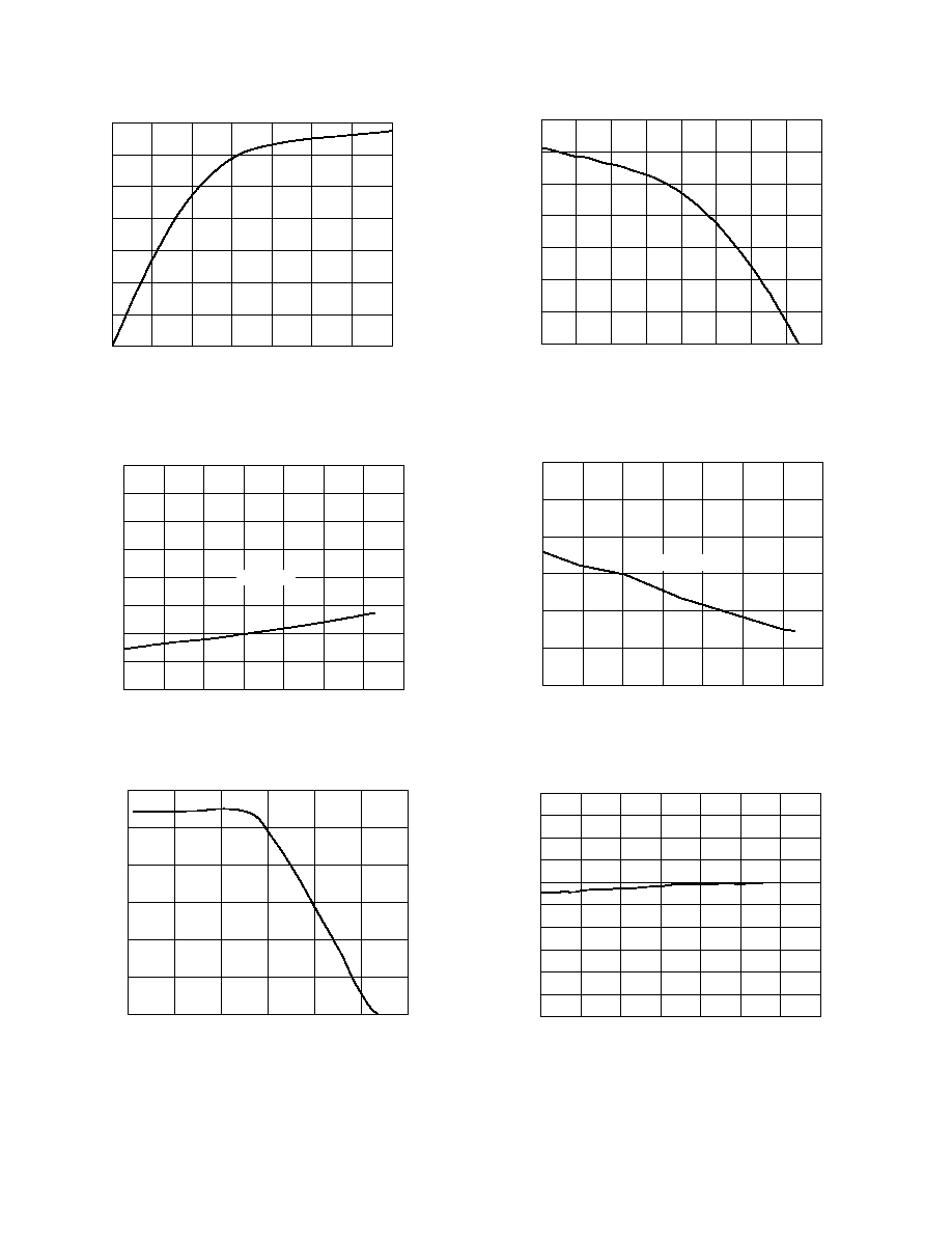
Figure 13. Receiver Output Low Voltage vs. Output
Current
TEMPERATURE C
40
100
20
0
20
40
60
80
0.8
0
0.7
0.4
0.3
0.2
0.1
0.6
0.5
I
RO
= 2.5mA
OUTPUT VOLTAGE V
Figure 14. Receiver Output Low Voltage vs. Temperature
DIFFERENTIAL O/P VOLTAGE Volts
120
0
0
3
0.5
1
1.5
2
2.5
100
80
60
40
20
OUTPUT CURRENT mA
Figure 15. Driver Differential Output Voltage vs. Output
Current
OUTPUT HIGH VOLTAGE Volts
14
0
0
4
0
1
1.5
2
2.5
3
3.5
12
8
6
4
2
10
.5
OUTPUT CURRENT mA
Figure 16. Receiver Output High Voltage vs. Output
Current
TEMPERATURE C
3.3
3
40
100
20
0
20
40
60
80
3.25
3.2
3.15
3.1
3.05
I
RO
= 1.5mA
OUTPUT VOLTAGE V
Figure 17. Receiver Output High Voltage vs. Temperature
TEMPERATURE C
2.6
1.6
40
100
20
0
20
40
60
80
2.5
2.0
1.9
1.8
1.7
2.3
2.1
2.4
2.2
OUTPUT VOLTAGE V
Figure 18. Driver Differential Output Voltage vs.
Temperature
Typical Performance Characteristics
ADM3491
9
REV. 0
TEMPERATURE C
1.2
1.1
0.7
40
100
20
0
20
40
60
80
1
0.9
0.8
SUPPLY CURRENT mA
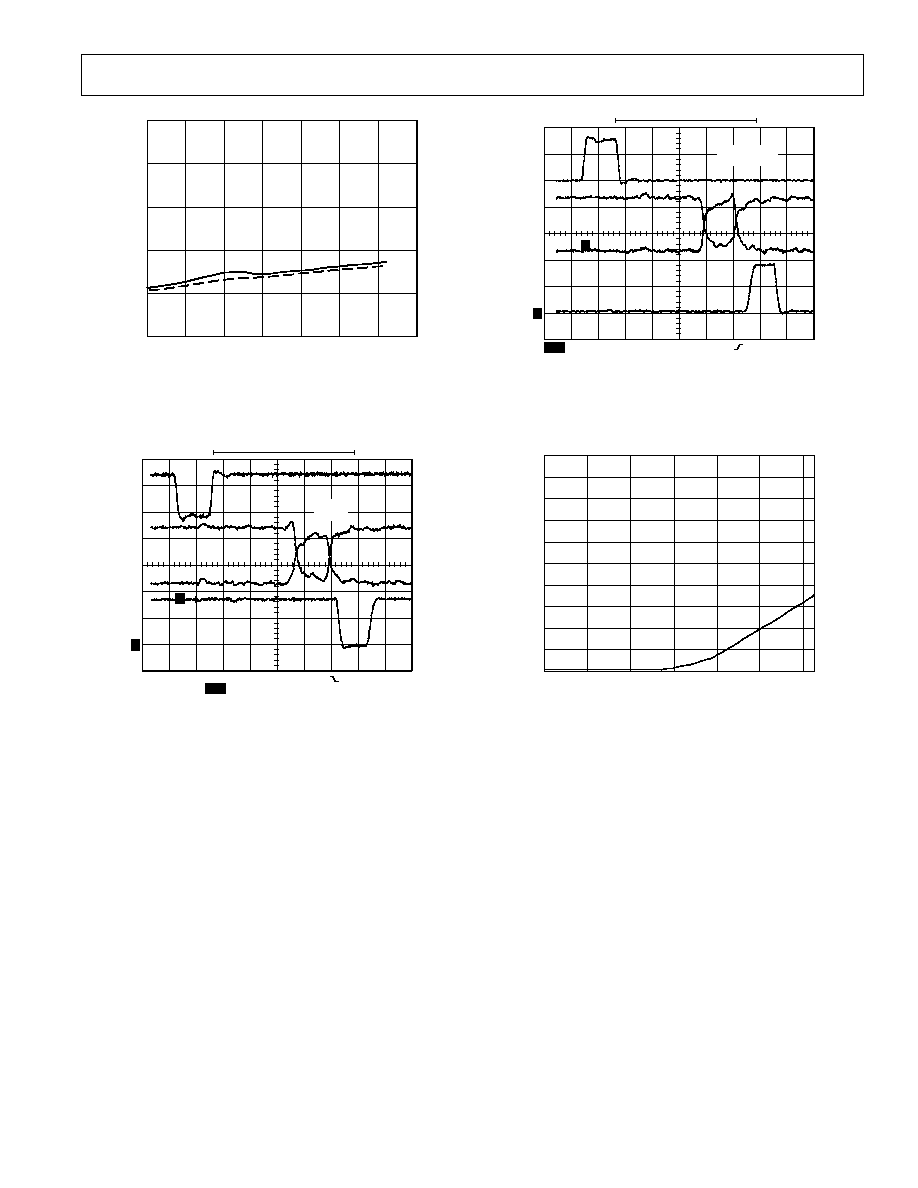
Figure 19. Supply Current vs. Temperature
3
2
1
T
T
T
4
T
100FT
CABLE
CH1 1.00V CH2 1.00V M40.0ns CH3 640mV
CH3 2.00V
CH4
2.00V
[ T ]
Figure 20. Driving 100 ft. Cable L-H Transition
3
2
1
T
T
T
4
T
100FT CAT 5
CABLE
CH1
1.00V CH2 1.00V M40.0ns CH3 640mV
CH3 2.00V CH4 2.00V
[ T ]
Figure 21. Driving 100 ft. Cable H-L Transition
TEMPERATURE C
100
0
40
80
20
0
20
40
60
90
60
30
20
10
80
70
50
40
SHUTDOWN CURRENT mA
Figure 22. Shutdown Current vs. Temperature
ADM3491
10
REV. 0
Table I. Transmitting Truth Table
Transmitting
Inputs
Outputs
RE
DE
DI
Z
Y
X
1
1
0
1
X
1
0
1
0
0
0
X
Hi-Z
Hi-Z
1
0
X
Hi-Z
Hi-Z
Table II. Receiving Truth Table
Receiving
Inputs
Outputs
RE
DE
AB
RO
0
X
> +0.2 V
1
0
X
< 0.2 V
0
0
X
Inputs O/C
1
1
X
X
Hi-Z
RE
V
CC
RO
R
A
B
Z
Y
GND
DE
DI
ADM3491
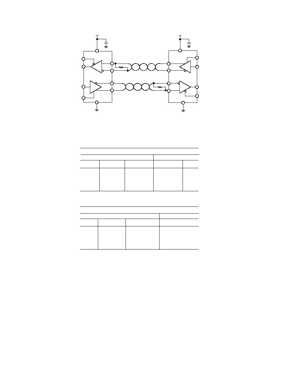
RS-485/RS-422 LINK
ADM3491
GND
RE
RO
DI
DE
V
CC
Y
Z
A
+3.3V
0.1 F
0.1 F
+3.3V
B
D
D
R
Figure 23. ADM3491 Full-Duplex Data Link
ADM3491
11
REV. 0
Table III. Comparison of RS-422 and RS-485 Interface Standards
Specification
RS-422
RS-485
Transmission Type
Differential
Differential
Maximum Cable Length
4000 ft.
4000 ft.
Minimum Driver Output Voltage
±
2 V
±
1.5 V
Driver Load Impedance
100
54
Receiver Input Resistance
4 k
min
12 k
min
Receiver Input Sensitivity
±
200 mV
±
200 mV
Receiver Input Voltage Range
7 V to +7 V
7 V to +12 V
APPLICATIONS INFORMATION
Differential Data Transmission
Differential data transmission is used to reliably transmit data at
high rates over long distances and through noisy environments.
Differential transmission nullifies the effects of ground shifts
and noise signals which appear as common-mode voltages on
the line.
Two main standards are approved by the Electronics Industries
Association (EIA) which specify the electrical characteristics of
transceivers used in differential data transmission. The RS-422
standard specifies data rates up to 10 MBaud and line lengths
up to 4000 ft. A single driver can drive a transmission line with
up to 10 receivers.
The RS-485 standard was defined to cater to true multipoint
communications. This standard meets or exceeds all the re-
quirements of RS-422, but also allows multiple drivers and
receivers to be connected to a single bus. An extended common
mode range of 7 V to +12 V is defined.
The most significant difference between RS-422 and RS-485 is
the fact that the drivers may be disabled thereby allowing more
than one to be connected to a single line. Only one driver should
be enabled at a time, but the RS-485 standard contains addi-
tional specifications to guarantee device safety in the event of
line contention.
Cable and Data Rate
The transmission line of choice for RS-485 communications is a
twisted pair. Twisted pair cable tends to cancel common-mode
noise and also causes cancellation of the magnetic fields gener-
ated by the current flowing through each wire, thereby reducing
the effective inductance of the pair.
The ADM3491 is designed for bidirectional data communica-
tions on multipoint transmission lines. A typical application
showing a multipoint transmission network is illustrated in
Figure 23. Only one driver can transmit at a particular time, but
multiple receivers may be enabled simultaneously.
As with any transmission line, it is important that reflections are
minimized. This may be achieved by terminating the extreme
ends of the line using resistors equal to the characteristic im-
pedance of the line. Stub lengths of the main line should also be
kept as short as possible. A properly terminated transmission
line appears purely resistive to the driver.
Receiver Open-Circuit Fail Safe
The receiver input includes a fail-safe feature that guarantees a
logic high on the receiver when the inputs are open circuit or
floating.
ADM3491
12
REV. 0
C321681/98
PRINTED IN U.S.A.
OUTLINE DIMENSIONS
Dimensions shown in inches and (mm).
14-Lead Plastic DIP
(N-14)
14
1
7
8
0.795 (20.19)
0.725 (18.42)
0.280 (7.11)
0.240 (6.10)
PIN 1
0.325 (8.25)
0.300 (7.62)
0.015 (0.381)
0.008 (0.204)
0.195 (4.95)
0.115 (2.93)
SEATING
PLANE
0.022 (0.558)
0.014 (0.356)
0.060 (1.52)
0.015 (0.38)
0.210 (5.33)
MAX
0.130
(3.30)
MIN
0.070 (1.77)
0.045 (1.15)
0.100
(2.54)
BSC
0.160 (4.06)
0.115 (2.93)
14-Lead Narrow Body Small Outline (SOIC)
(R-14)
14
8
7
1
0.3444 (8.75)
0.3367 (8.55)
0.2440 (6.20)
0.2284 (5.80)
0.1574 (4.00)
0.1497 (3.80)
PIN 1
SEATING
PLANE
0.0098 (0.25)
0.0040 (0.10)
0.0192 (0.49)
0.0138 (0.35)
0.0688 (1.75)
0.0532 (1.35)
0.0500
(1.27)
BSC
0.0099 (0.25)
0.0075 (0.19)
0.0500 (1.27)
0.0160 (0.41)
8
°
0
°
0.0196 (0.50)
0.0099 (0.25)
x 45
°
16-Lead Thin Shrink Small Outline (TSSOP)
(RU-16)
16
9
8
1
0.201 (5.10)
0.193 (4.90)
0.256 (6.50)
0.246 (6.25)
0.177 (4.50)
0.169 (4.30)
PIN 1
SEATING
PLANE
0.006 (0.15)
0.002 (0.05)
0.0118 (0.30)
0.0075 (0.19)
0.0256
(0.65)
BSC
0.0433
(1.10)
MAX
0.0079 (0.20)
0.0035 (0.090)
0.028 (0.70)
0.020 (0.50)
8
°
0
°