 | –≠–ª–µ–∫—Ç—Ä–æ–Ω–Ω—ã–π –∫–æ–º–ø–æ–Ω–µ–Ω—Ç: ADM483EAN | –°–∫–∞—á–∞—Ç—å:  PDF PDF  ZIP ZIP |

REV. 0
Information furnished by Analog Devices is believed to be accurate and
reliable. However, no responsibility is assumed by Analog Devices for its
use, nor for any infringements of patents or other rights of third parties
which may result from its use. No license is granted by implication or
otherwise under any patent or patent rights of Analog Devices.
a
ADM483E
One Technology Way, P.O. Box 9106, Norwood, MA 02062-9106, U.S.A.
Tel: 617/329-4700
World Wide Web Site: http://www.analog.com
Fax: 617/326-8703
© Analog Devices, Inc., 1997
15 kV ESD Protected, EMC Compliant
Slew Rate Limited, EIA RS-485 Transceiver
FUNCTIONAL BLOCK DIAGRAM
FEATURES
Robust RS-485 Transceiver
15 kV ESD Protection Using HBM
2 kV EFT Protection Meets IEC1000-4-4
High EM Immunity Meets IEC1000-4-3
Reduced Slew Rate for Low EM Interference
250 kbps Data Rate
Single +5 V 10% Supply
≠7 V to +12 V Bus Common-Mode Range
12 k Input Impedance
Short Circuit Protection
Excellent Noise Immunity
36 A Supply Current
0.1 A Shutdown Current
APPLICATIONS
Low Power RS-485 Systems
Electrically Harsh Environments
EMI Sensitive Applications
DTE-DCE Interface
Packet Switching
Local Area Networks
D
R
A
B
DI
DE
RE
RO
ADM483E
GENERAL DESCRIPTION
The ADM483E is a robust, low power differential line trans-
ceiver suitable for communication on multipoint bus transmis-
sion lines. Internal protection against electrostatic discharge
(ESD), electrical fast transient (EFT) and electromagnetic
immunity (EMI) allows operation in electrically harsh environ-
ments. ESD protection on the I-O lines meets
±
15 kV when
tested using the Human Body Model. EFT protection meets
±
2 kV in accordance with IEC1000-4-4, while EMI immunity is
in excess of 10 V/m meeting IEC1000-4-3.
The level of unwanted emissions is also carefully controlled
using slew limiting on the driver outputs. This reduces reflec-
tions with improperly terminated cables and also minimizes
electromagnetic interference. The controlled slew rate limits the
data rate to 250 kbps.
The ADM483E is intended for balanced data transmission and
complies with both EIA Standards RS-485 and RS-422. It
contains a differential line driver and a differential line receiver
and is suitable for half duplex data transmission, as the driver
and receiver share the same differential pins.
The input impedance on the ADM483E is 12 k
, allowing up
to 32 transceivers on the bus.
The ADM483E operates from a single +5 V
±
10% power sup-
ply. Excessive power dissipation caused by bus contention or by
output shorting is prevented by a thermal shutdown circuit. This
feature forces the driver output into a high impedance state if,
during fault conditions, a significant temperature increase is
detected in the internal driver circuitry.
The receiver contains a fail-safe feature that results in a logic
high output state if the inputs are unconnected (floating).
The ADM483E is fabricated on BiCMOS, an advanced mixed
technology process combining low power CMOS with robust
bipolar technology.
It is fully specified over the industrial temperature range and is
available in 8-lead DIP and SOIC packages.

≠2≠
REV. 0
ADM483E≠SPECIFICATIONS
Parameter
Min
Typ
Max
Units
Test Conditions/Comments
DRIVER
Differential Output Voltage, V
OD
5.0
V
V
CC
= 5.25 V. R =
, Figure 1
2.0
5.0
V
R = 50
(RS-422), Figure 1
1.5
5.0
V
R = 27
(RS-485), Figure 1
1.5
5.0
V
V
TST
= ≠7 V to +12 V, Figure 2, V
CC
4.75 V
|V
OD
| for Complementary Output States
0.2
V
R = 27
or 50
, Figure 1
Common-Mode Output Voltage V
OC
3
V
R = 27
or 50
, Figure 1
|V
OC
| for Complementary Output States
0.2
V
R = 27
or 50
Output Short Circuit Current (V
OUT
= High)
250
mA
≠7 V
V
O
+12 V
Output Short Circuit Current (V
OUT
= Low)
250
mA
≠7 V
V
O
+12 V
CMOS Input Logic Threshold Low, V
INL
1.4
0.8
V
CMOS Input Logic Threshold High, V
INH
2.0
1.4
V
Logic Input Current (DE, DI)
±
1.0
µ
A
RECEIVER
Differential Input Threshold Voltage, V
TH
≠0.2
+0.2
V
≠7 V
V
CM
+12 V
Input Voltage Hysteresis,
V
TH
70
mV
V
CM
= 0 V
Input Resistance
12
k
≠7 V
V
CM
+12 V
Input Current (A, B)
+1
mA
V
IN
= 12 V
≠0.8
mA
V
IN
= ≠7 V
Logic Enable Input Current (RE)
±
1
µ
A
CMOS Output Voltage Low, V
OL
0.4
V
I
OUT
= +4.0 mA
CMOS Output Voltage High, V
OH
4.0
V
I
OUT
= ≠4.0 mA
Short Circuit Output Current
7
85
mA
V
OUT
= GND or V
CC
Three-State Output Leakage Current
±
1.0
µ
A
0.4 V
V
OUT
+2.4 V
POWER SUPPLY CURRENT
Outputs Unloaded, Receivers Enabled
I
CC
(ADM483E)
36
60
µ
A
DE = 0 V (Disabled) RE = 0 V
270
360
µ
A
DE = 5 V (Enabled) = RE = 0 V
Supply Current in Shutdown
0.1
10
µ
A
DE = 0 V, RE = V
CC
ESD/EFT IMMUNITY
ESD Protection
±
15
kV
HBM Air Discharge. A, B Pins
±
3.5
kV
HBM 3015.7 Contact Discharge. All Pins
EFT Protection
±
2
kV
IEC1000-4-4, A, B Pins
EMI Immunity
10
V/m
IEC1000-4-3
Specifications subject to change without notice.
TIMING SPECIFICATIONS
Parameter
Min
Typ
Max
Units
Test Conditions/Comments
DRIVER
Propagation Delay Input to Output T
PLH
, T
PHL
250
2000
ns
R
L
Diff = 54
C
L1
= C
L2
= 100 pF, Figure 5
Driver O/P to O/P T
SKEW
100
800
ns
R
L
Diff = 54
C
L1
= C
L2
= 100 pF, Figure 5
Driver Rise/Fall Time T
R
, T
F
250
2000
ns
R
L
Diff = 54
C
L1
= C
L2
= 100 pF, Figure 5
Driver Enable to Output Valid
250
2000
ns
R
L
= 500
, C
L
= 100 pF, Figure 3
Driver Disable Timing
300
3000
ns
R
L
= 500
, C
L
= 15 pF, Figure 3
RECEIVER
Propagation Delay Input to Output T
PLH
, T
PHL
250
2000
ns
C
L
= 15 pF, Figure 5
Skew |T
PLH
≠T
PHL
|
200
ns
Receiver Enable T
EN1
10
50
ns
R
L
= 1 k
, C
L
= 15 pF, Figure 4
Receiver Disable T
EN2
10
50
ns
R
L
= 1 k
, C
L
= 15 pF, Figure 4
SHUTDOWN
Time to Shutdown
50
200
600
ns
Driver Enable from Shutdown
2000
ns
R
L
= 500
, C
L
= 100 pF, Figure 3
Receiver Enable from Shutdown
2500
ns
R
L
= 1 k
, C
L
= 15 pF, Figure 4
Specifications subject to change without notice.
(V
CC
= +5 V 10%. All specifications T
MIN
to T
MAX
unless otherwise noted)
(V
CC
= +5 V 10%. All specifications T
MIN
to T
MAX
unless otherwise noted.)

ADM483E
≠3≠
REV. 0
ABSOLUTE MAXIMUM RATINGS*
(T
A
= +25
∞
C unless otherwise noted)
V
CC
. . . . . . . . . . . . . . . . . . . . . . . . . . . . . . . . . . . . . . . . . .+7 V
Inputs
Driver Input (DI) . . . . . . . . . . . . . . . . ≠0.5 V to V
CC
+ 0.5 V
Control Inputs (DE, RE) . . . . . . . . . . ≠0.5 V to V
CC
+ 0.5 V
Receiver Inputs (A, B) . . . . . . . . . . . . . . . . . ≠14 V to +14 V
Outputs
Driver Outputs . . . . . . . . . . . . . . . . . . . . ≠12.5 V to +12.5 V
Receiver Output . . . . . . . . . . . . . . . . . ≠0.5 V to V
CC
+0.5 V
ESD Rating: Air (Human Body Model) (A, B Pins) . .
±
15 kV
ESD Rating: Contact (Human Body Model)
(A, B Pins) . . . . . . . . . . . . . . . . . . . . . . . . . . . . . . . . .
±
8 kV
ESD Rating MIL-STD-883B Method 3015
(Except A, B) . . . . . . . . . . . . . . . . . . . . . . . . . . . . . .
±
3.5 kV
EFT Rating (IEC1000-4-4) (A, B Pins) . . . . . . . . . . . .
±
2 kV
EMI Immunity (IEC1000-4-3) . . . . . . . . . . . . . . . . . . 10 V/m
Power Dissipation 8-Pin DIP . . . . . . . . . . . . . . . . . . . 727 mW
JA
, Thermal Impedance . . . . . . . . . . . . . . . . . . +135
∞
C/W
Power Dissipation 8-Pin SOIC . . . . . . . . . . . . . . . . . 470 mW
JA
, Thermal Impedance . . . . . . . . . . . . . . . . . . +110
∞
C/W
Operating Temperature Range
Industrial (A Version) . . . . . . . . . . . . . . . . ≠40
∞
C to +85
∞
C
Storage Temperature Range . . . . . . . . . . . ≠65
∞
C to +150
∞
C
Lead Temperature (Soldering, 10 sec) . . . . . . . . . . . . +300
∞
C
Vapor Phase (60 sec) . . . . . . . . . . . . . . . . . . . . . . . . +215
∞
C
Infrared (15 sec) . . . . . . . . . . . . . . . . . . . . . . . . . . . . +220
∞
C
*Stresses above those listed under "Absolute Maximum Ratings" may cause
permanent damage to the device. This is a stress rating only; functional operation
of the device at these or any other conditions above those indicated in the
operational sections of this specification is not implied. Exposure to absolute
maximum ratings for extended periods may affect device reliability.
ORDERING GUIDE
Model
Temperature Range
Package Option
ADM483EAN
≠40
∞
C to +85
∞
C
N-8
ADM483EAR
≠40
∞
C to +85
∞
C
SO-8
PIN FUNCTION DESCRIPTION
Pin Mnemonic Function
1
RO
Receiver Output. When enabled if A > B by
200 mV, then RO = High. If A < B by
200 mV, then RO = Low.
2
RE
Receiver Output Enable. A low level enables
the receiver output, RO. A high level places it
in a high impedance state.
3
DE
Driver Output Enable. A high level enables
the driver differential outputs, A and B. A
low level places it in a high impedance state.
4
DI
Driver Input. When the driver is enabled a
logic Low on DI forces A low and B high
while a logic High on DI forces A high and B
low.
5
GND
Ground Connection, 0 V.
6
A
Noninverting Receiver Input A/Driver
Output A.
7
B
Inverting Receiver Input B/Driver Output B.
8
V
CC
Power Supply, 5 V
±
10%.
PIN CONFIGURATION
RE
DE
DI
V
CC
B
A
GND
1
2
3
4
8
7
6
5
TOP VIEW
(Not to Scale)
ADM483E
RO
Table I. Selection Table
Part No.
Duplex
Data Rate
Low Power
Tx/Rx
I
CC
No of Tx/Rx
ESD
EFT
EMI
kb/s
Shutdown
Enable
A
On Bus
kV
kV
V/m
ADM483E
Half
250
Yes
Yes
36
32
±
15
±
2
10

≠4≠
REV. 0
ADM483E
V
OD
V
OC
R
R
Figure 1. Driver Voltage Measurement Test Circuit
V
OD3
V
TST
60
375
375
Figure 2. Driver Voltage Measurement Test Circuit 2
R
L
S1
S2
V
CC
C
L
V
OUT
A
B
0V OR 3V
DE IN
DE
Figure 3. Driver Enable/Disable Test Circuit
R
L
S2
V
CC
C
L
V
OUT
RE IN
RE
S1
+15V
≠15V
Figure 4. Receiver Enable/Disable Test Circuit
Test Circuits
≠VO
VO
1/2VO
0V
3V
1.5V
1.5V
T
PLH
T
SKEW
VO
0V
90% POINT
10% POINT
90% POINT
10% POINT
T
PHL
B
A
T
SKEW
T
R
T
F
Figure 6. Driver Propagation Delay, Rise/Fall Timing
T
PLH
T
PHL
0V
0V
1.5V
1.5V
A≠B
RO
V
OL
V
OH
Figure 8. Receiver Propagation Delay
Switching Characteristics
RL
DIFF
C
L1
C
L2
D
R
RO
RE
A
B
DI
Figure 5. Receiver Propagation Delay Test Circuit
T
ZH
1.5V
DE
1.5V
3V
0V
2.3V
T
HZ
V
OH
V
OH
≠ 0.5V
0V
A, B
V
OL
+ 0.5V
T
ZL
2.3V
T
LZ
V
OL
A, B
Figure 7. Driver Enable/Disable Timing
T
ZH
1.5V
1.5V
3V
0V
1.5V
T
HZ
V
OH
V
OH
≠ 0.5V
0V
R
V
OL
+ 0.5V
T
ZL
1.5V
T
LZ
V
OL
R
RE
O/P LOW
O/P HIGH
Figure 9. Receiver Enable/Disable Timing
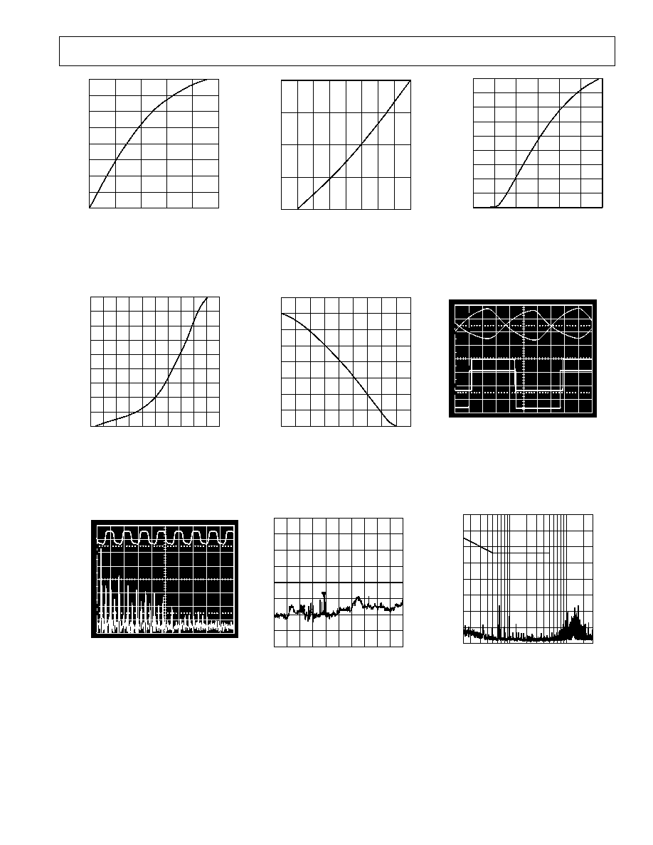
Typical Performance Characteristics≠ADM483E
REV. 0
≠5≠
OUTPUT VOLTAGE ≠ Volts
40
35
0
0
0.5
2.5
1.0
1.5
2.0
20
15
10
5
30
25
OUTPUT CURRENT ≠ mA
Figure 11. Receiver Output Low
Voltage vs. Output Current
OUTPUT VOLTAGE ≠ Volts
0
0.5
5.0
1.0 1.5 2.0 2.5 3.0 3.5 4.0 4.5
0
OUTPUT CURRENT ≠ mA
≠10
≠90
≠50
≠60
≠70
≠80
≠20
≠40
≠30
Figure 14. Driver Output High
Voltage vs. Output Current
10
0%
100
90
10dB/DIV
500kHz/DIV
0
5MHz
Figure 17. Driver Output Waveform
and FFT Plot Transmitting @ 150 kHz
OUTPUT VOLTAGE ≠ Volts
0
≠5
≠20
3.4
3.6
5.0
3.8
4.0
4.2
4.4
4.6
4.8
≠10
≠15
OUTPUT CURRENT ≠ mA
Figure 12. Receiver Output High
Voltage vs. Output Current
OUTPUT VOLTAGE ≠ Volts
80
0
0
0.5
4.5
1.0
1.5 2.0
3.0
3.5
4.0
2.5
70
40
30
20
10
60
50
OUTPUT CURRENT ≠ mA
Figure 15. Driver Differential Output
Voltage vs. Output Current
LIMIT
30
200
FREQUENCY ≠ MHz
80
70
60
50
40
30
20
10
0
dBµV
Figure 18. Radiated Emissions
OUTPUT VOLTAGE ≠ Volts
0
OUTPUT CURRENT ≠ mA
0.5
3.0
1.0
1.5
2.0
2.5
90
80
0
40
30
20
10
70
50
60
Figure 13. Driver Output Low
Voltage vs. Output Current
10
0%
100
90
T
T
T
RO
DI
Figure 16. ADM483E Driving
4000 ft. of Cable
LOG FREQUENCY (0.15≠30) ≠ MHz
0.3
0.6
1
3
6
10
30
80
0
70
40
30
20
10
60
50
LIMIT
dBµV
Figure 19. Conducted Emissions