 | ÐлекÑÑоннÑй компоненÑ: ADM488AN | СкаÑаÑÑ:  PDF PDF  ZIP ZIP |
Äîêóìåíòàöèÿ è îïèñàíèÿ www.docs.chipfind.ru
REV. 0
Information furnished by Analog Devices is believed to be accurate and
reliable. However, no responsibility is assumed by Analog Devices for its
use, nor for any infringements of patents or other rights of third parties
which may result from its use. No license is granted by implication or
otherwise under any patent or patent rights of Analog Devices.
a
ADM488/ADM489
One Technology Way, P.O. Box 9106, Norwood, MA 02062-9106, U.S.A.
Tel: 617/329-4700
World Wide Web Site: http://www.analog.com
Fax: 617/326-8703
© Analog Devices, Inc., 1997
Full-Duplex, Low Power,
Slew Rate Limited, EIA RS-485 Transceivers
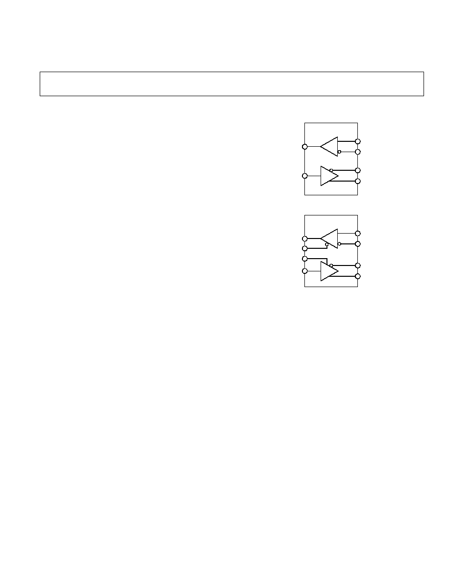
FUNCTIONAL BLOCK DIAGRAMS
FEATURES
Meets EIA RS-485 Standard
250 kbps Data Rate
Single +5 V
10% Supply
7 V to +12 V Bus Common-Mode Range
12 k Input Impedance
2 kV EFT Protection Meets IEC1000-4-4
High EM Immunity Meets IEC1000-4-3
Reduced Slew Rate for Low EM Interference
Short Circuit Protection
Excellent Noise Immunity
30
A Supply Current
APPLICATIONS
Low Power RS-485 Systems
DTE-DCE Interface
Packet Switching
Local Area Networks
Data Concentration
Data Multiplexers
Integrated Services Digital Network (ISDN)
GENERAL DESCRIPTION
The ADM488 and ADM489 are low power differential line
transceiver suitable for communication on multipoint bus trans-
mission lines.
They are intended for balanced data transmission and comply
with both EIA Standards RS-485 and RS-422. Both products
contains a single differential line driver and a single differential
line receiver making them suitable for full duplex data transfer.
The ADM489 contains an additional receiver and driver enable
control.
The input impedance is 12 k
, allowing 32 transceivers to be
connected on the bus.
The ADM488/ADM489 operates from a single +5 V
±
10%
power supply. Excessive power dissipation caused by bus con-
tention or by output shorting is prevented by a thermal shut-
down circuit. This feature forces the driver output into a high
impedance state if during fault conditions a significant tempera-
ture increase is detected in the internal driver circuitry.
The receiver contains a fail-safe feature that results in a logic
high output state if the inputs are unconnected (floating).
The ADM488/ADM489 is fabricated on BiCMOS, an ad-
vanced mixed technology process combining low power CMOS
with fast switching bipolar technology.
The ADM488/ADM489 is fully specified over the industrial
temperature range and is available in DIP, SOIC and TSSOP
packages.
ADM488
R
D
RO
DI
A
B
Z
Y
ADM489
R
D
RO
DI
A
B
Z
Y
RE
DE

2
REV. 0
ADM488/ADM489SPECIFICATIONS
(V
CC
= +5 V 10%. All specifications T
MIN
to T
MAX
unless
otherwise noted)
Parameter
Min
Typ
Max
Units
Test Conditions/Comments
DRIVER
Differential Output Voltage, V
OD
5.0
V
R =
, Figure 1
2.0
5.0
V
V
CC
= 5 V, R = 50
(RS-422), Figure 1
1.5
5.0
V
R = 27
(RS-485), Figure 1
1.5
5.0
V
V
TST
= 7 V to +12 V, Figure 2, V
CC
= 5 V
±
5%
|V
OD
| for Complementary Output States
0.2
V
R = 27
or 50
, Figure 1
Common-Mode Output Voltage V
OC
3
V
R = 27
or 50
, Figure 1
|V
OC
| for Complementary Output States
0.2
V
R = 27
or 50
Output Short Circuit Current (V
OUT
= High)
250
mA
7 V
V
O
+12 V
Output Short Circuit Current (V
OUT
= Low)
250
mA
7 V
V
O
+12 V
CMOS Input Logic Threshold Low, V
INL
1.4
0.8
V
CMOS Input Logic Threshold High, V
INH
2.0
1.4
V
Logic Input Current (DE, DI)
±
1.0
µ
A
RECEIVER
Differential Input Threshold Voltage, V
TH
0.2
+0.2
V
7 V
V
CM
+12 V
Input Voltage Hysteresis,
V
TH
70
mV
V
CM
= 0 V
Input Resistance
12
k
7 V
V
CM
+12 V
Input Current (A, B)
+1
mA
V
IN
= 12 V
0.8
mA
V
IN
= 7 V
Logic Enable Input Current (
RE)
±
1
µ
A
CMOS Output Voltage Low, V
OL
0.4
V
I
OUT
= +4.0 mA
CMOS Output Voltage High, V
OH
4.0
V
I
OUT
= 4.0 mA
Short Circuit Output Current
7
85
mA
V
OUT
= GND or V
CC
Three-State Output Leakage Current
±
1.0
µ
A
0.4 V
V
OUT
+2.4 V
POWER SUPPLY CURRENT
Outputs Unloaded, Receivers Enabled
I
CC
30
60
µ
A
DE = 0 V (Disabled)
37
74
µ
A
DE = 5 V (Enabled)
Specifications subject to change without notice.
TIMING SPECIFICATIONS
Parameter
Min
Typ
Max
Units
Test Conditions/Comments
DRIVER
Propagation Delay Input to Output T
PLH
, T
PHL
250
2000
ns
R
L
Diff = 54
, C
L1
= C
L2
= 100 pF, Figure 5
Driver O/P to
O/P T
SKEW
100
800
ns
R
L
Diff = 54
, C
L1
= C
L2
= 100 pF, Figure 5
Driver Rise/Fall Time T
R
, T
F
250
2000
ns
R
L
Diff = 54
, C
L1
= C
L2
= 100 pF, Figure 5
Driver Enable to Output Valid
250
2000
ns
R
L
= 500
, C
L
= 100 pF, Figure 2
Driver Disable Timing
300
3000
ns
R
L
= 500
, C
L
= 15 pF, Figure 2
Data Rate
250
kbps
RECEIVER
Propagation Delay Input to Output T
PLH
, T
PHL
250
2000
ns
C
L
= 15 pF, Figure 5
Skew |T
PLH
T
PHL
|
100
ns
Receiver Enable T
EN1
10
50
ns
R
L
= 1 k
, C
L
= 15 pF, Figure 4
Receiver Disable T
EN2
10
50
ns
R
L
= 1 k
, C
L
= 15 pF, Figure 4
Data Rate
250
kbps
Specifications subject to change without notice.
(V
CC
= +5 V 10%. All specifications T
MIN
to T
MAX
unless otherwise noted)

ADM488/ADM489
3
REV. 0
ABSOLUTE MAXIMUM RATINGS*
(T
A
= +25
°
C unless otherwise noted)
V
CC
. . . . . . . . . . . . . . . . . . . . . . . . . . . . . . . . . . . . . . . . +7 V
Inputs
Driver Input (DI) . . . . . . . . . . . . . . . 0.3 V to V
CC
+ 0.3 V
Control Inputs (DE,
RE) . . . . . . . . . 0.3 V to V
CC
+ 0.3 V
Receiver Inputs (A, B) . . . . . . . . . . . . . . . . 14 V to +14 V
Outputs
Driver Outputs . . . . . . . . . . . . . . . . . . . . . 14 V to +12.5 V
Receiver Output . . . . . . . . . . . . . . . . 0.5 V to V
CC
+ 0.5 V
Power Dissipation 8-Lead DIP . . . . . . . . . . . . . . . . . 700 mW
JA
, Thermal Impedance . . . . . . . . . . . . . . . . . . . 120
°
C/W
Power Dissipation 8-Lead SOIC . . . . . . . . . . . . . . . . 520 mW
JA
, Thermal Impedance . . . . . . . . . . . . . . . . . . . 110
°
C/W
Power Dissipation 14-Lead DIP . . . . . . . . . . . . . . . . 800 mW
JA
, Thermal Impedance . . . . . . . . . . . . . . . . . . . 140
°
C/W
Power Dissipation 14-Lead SOIC . . . . . . . . . . . . . . . 800 mW
JA
, Thermal Impedance . . . . . . . . . . . . . . . . . . . 120
°
C/W
ORDERING GUIDE
Model
Temperature Range
Package Description
Package Option
ADM488AR
40
°
C to +85
°
C
8-Lead Narrow Body (SOIC)
SO-8
ADM488AN
40
°
C to +85
°
C
8-Lead Plastic DIP
N-8
ADM489AN
40
°
C to +85
°
C
14-Lead Plastic DIP (Narrow)
N-14
ADM489AR
40
°
C to +85
°
C
14-Lead Narrow Body (SOIC)
R-14
ADM489ARU
40
°
C to +85
°
C
16-Lead Thin Shrink Small Outline Package (TSSOP)
RU-16
Power Dissipation 16-Lead TSSOP . . . . . . . . . . . . . . 800 mW
JA
, Thermal Impedance . . . . . . . . . . . . . . . . . . . 150
°
C/W
Operating Temperature Range
Industrial (A Version) . . . . . . . . . . . . . . . 40
°
C to +85
°
C
Storage Temperature Range . . . . . . . . . . . . 65
°
C to +150
°
C
Lead Temperature (Soldering, 10 secs) . . . . . . . . . . . +300
°
C
Vapor Phase (60 secs) . . . . . . . . . . . . . . . . . . . . . . +215
°
C
Infrared (15 secs) . . . . . . . . . . . . . . . . . . . . . . . . . . . +220
°
C
ESD Rating, MIL-STD-883B . . . . . . . . . . . . . . . . . . . . . 4 kV
EFT Rating, IEC1000-4-4 . . . . . . . . . . . . . . . . . . . . . . . 2 kV
*Stresses above those listed under Absolute Maximum Ratings may cause perma-
nent damage to the device. This is a stress rating only; functional operation of the
device at these or any other conditions above those listed in the operational
sections of this specification is not implied. Exposure to absolute maximum ratings
for extended periods of time may affect device reliability.
ADM488/ADM489
4
REV. 0
ADM488 PIN FUNCTION DESCRIPTIONS
Pin
Mnemonic
Function
1
V
CC
Power Supply, 5 V
±
10%.
2
RO
Receiver Output. When A > B by 200 mV,
RO = high. If A < B by 200 mV, RO = low.
3
DI
Driver Input. A logic Low on DI forces Y low
and Z high while a logic High on DI forces Y
high and Z low.
4
GND
Ground Connection, 0 V
5
Y
Noninverting Driver, Output Y
6
Z
Inverting Driver, Output Z
7
B
Inverting Receiver Input B
8
A
Noninverting Receiver Input A
ADM489 PIN FUNCTION DESCRIPTIONS
DIP/SOIC
TSSOP
Pin
Pin
Mnemonic Function
1, 8, 13
2, 9, 10,
NC
No Connect. No connections
13, 16
are required to this pin.
2
3
RO
Receiver Output. When
enabled if A > B by 200 mV
then RO = high. If A < B by
200 mV then RO = low.
3
4
RE
Receiver Output Enable. A
low level enables the receiver
output, RO. A high level
places it in a high impedance
state.
4
5
DE
Driver Output Enable. A
high level enables the driver
differential outputs, Y and Z.
A low level places it in a high
impedance state.
5
6
DI
Driver Input. When the
driver is enabled, a logic Low
on DI forces Y low and Z
high, while a logic High on
DI forces Y high and Z low.
6, 7
7, 8
GND
Ground Connection, 0 V
9
11
Y
Noninverting Driver
Output Y
10
12
Z
Inverting Driver Output Z
11
14
B
Inverting Receiver Input B
12
15
A
Noninverting Receiver
Input A
14
1
V
CC
Power Supply, 5 V
±
10%.
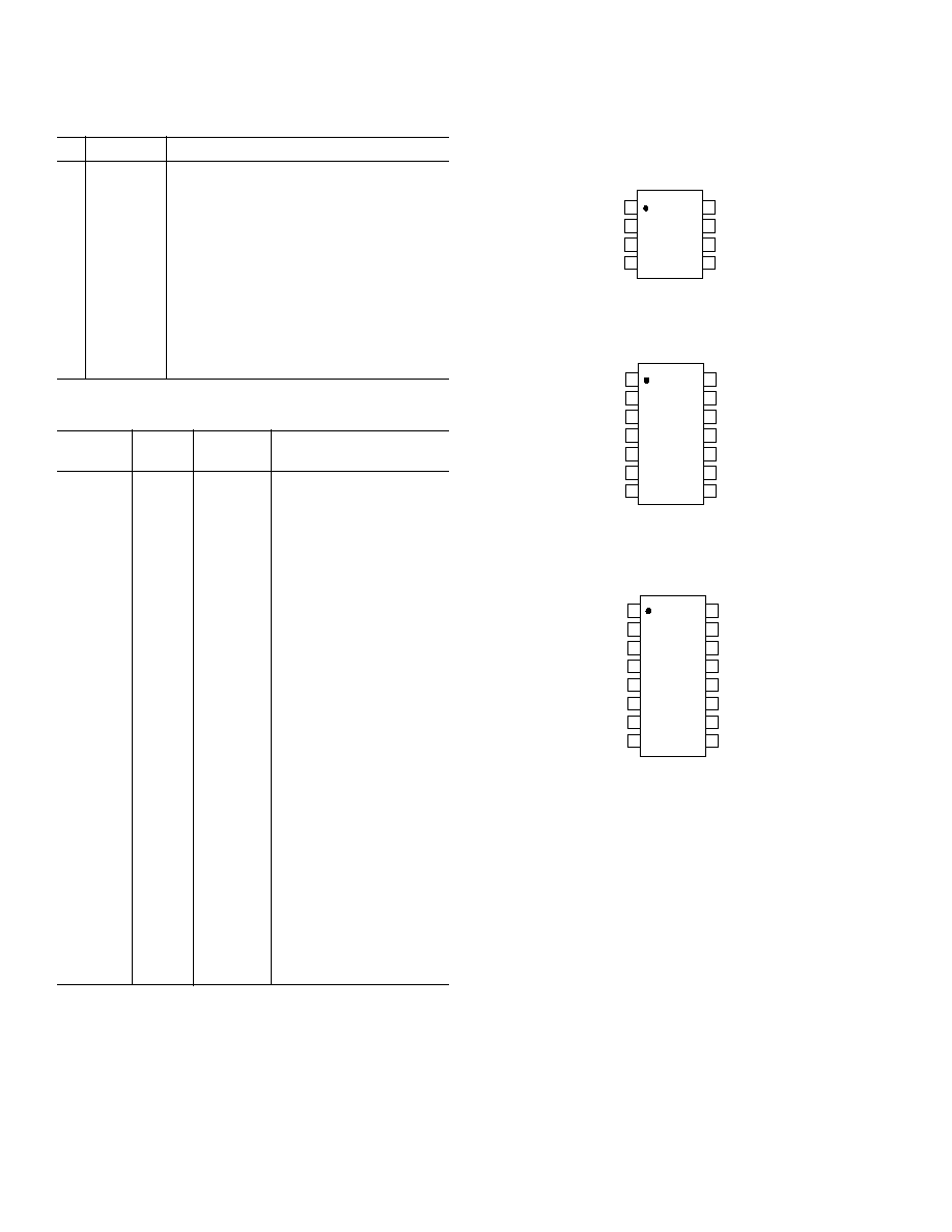
PIN CONFIGURATIONS
8-Lead DIP/SO
1
2
3
4
8
7
6
5
TOP VIEW
(Not to Scale)
ADM488
V
CC
Y
Z
B
A
RO
DI
GND
14-Lead DIP/SO
14
13
12
11
10
9
8
1
2
3
4
7
6
5
TOP VIEW
(Not to Scale)
NC = NO CONNECT
NC
B
A
NC
V
CC
RO
RE
DE
ADM489
NC
Y
Z
DI
GND
GND
16-Lead TSSOP
14
13
12
11
16
15
10
9
8
1
2
3
4
7
6
5
TOP VIEW
(Not to Scale)
ADM489
NC = NO CONNECT
V
CC
NC
B
A
NC
NC
RO
RE
NC
Y
Z
DE
DI
GND
GND
NC
ADM488/ADM489
5
REV. 0
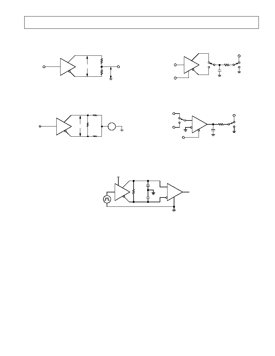
V
OD
V
OC
R
R
Figure 1. Driver Voltage Measurement Test Circuit
V
OD3
V
TST
60
375
375
Figure 2. Driver Enable/Disable Test Circuit
Test Circuits
R
L
S1
S2
V
CC
C
L
V
OUT
A
B
0V OR 3V
DE IN
DE
Figure 3. Driver Voltage Measurement Test Circuit 2
R
L
S2
V
CC
C
L
V
OUT
RE IN
RE
S1
+1.5V
1.5V
Figure 4. Receiver Enable/Disable Test Circuit
RL
DIFF
C
L1
C
L2
D
R
RO
RE
A
B
DI
+3V
DE
Y
Z
Figure 5. Driver/Receiver Propagation Delay Test Circuit
ADM488/ADM489
6
REV. 0
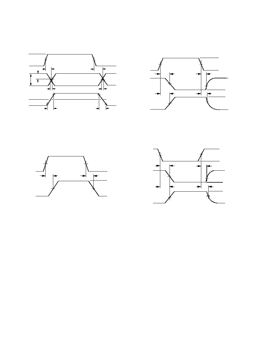
Switching Characteristics
VO
VO
1/2VO
0V
3V
1.5V
1.5V
T
PLH
T
SKEW
+VO
0V
90% POINT
10% POINT
90% POINT
10% POINT
T
PHL
B
A
T
SKEW
T
R
T
F
Figure 6. Driver Propagation Delay, Rise/Fall Timing
T
PLH
T
PHL
0V
0V
1.5V
1.5V
AB
RO
V
OL
V
OH
Figure 7. Receiver Propagation Delay
T
ZH
1.5V
DE
1.5V
3V
0V
2.3V
T
HZ
V
OH
V
OH
0.5V
0V
A, B
V
OL
+ 0.5V
T
ZL
2.3V
T
LZ
V
OL
A, B
Figure 8. Driver Enable/Disable Timing
T
ZH
1.5V
1.5V
3V
0V
1.5V
T
HZ
V
OH
V
OH
0.5V
0V
R
V
OL
+ 0.5V
T
ZL
1.5V
T
LZ
V
OL
R
RE
O/P LOW
O/P HIGH
Figure 9. Receiver Enable/Disable Timing
ADM488/ADM489
7
REV. 0
Typical Performance Characteristics
OUTPUT VOLTAGE Volts
40
35
0
0
0.5
2.5
1.0
1.5
2.0
20
15
10
5
30
25
OUTPUT CURRENT mA
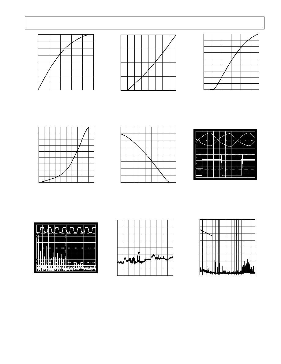
Figure 10. Receiver Output Low
Voltage vs. Output Current
OUTPUT VOLTAGE Volts
0
0.5
5.0
1.0 1.5 2.0 2.5 3.0 3.5 4.0 4.5
0
OUTPUT CURRENT mA
10
90
50
60
70
80
20
40
30
Figure 13. Driver Output High
Voltage vs. Output Current
Figure 16. Driver Output Waveform
and FFT Plot Transmitting @ 150 kHz
10
0%
100
90
T
T
T
RO
DI
10
0%
100
90
10dB/DIV
500kHz/DIV
0
5MHz
OUTPUT VOLTAGE Volts
0
5
20
3.4
3.6
5.0
3.8
4.0
4.2
4.4
4.6
4.8
10
15
OUTPUT CURRENT mA
Figure 11. Receiver Output High
Voltage vs. Output Current
OUTPUT VOLTAGE Volts
80
0
0
0.5
4.5
1.0
1.5 2.0
3.0
3.5
4.0
2.5
70
40
30
20
10
60
50
OUTPUT CURRENT mA
Figure 14. Driver Differential Output
Voltage vs. Output Current
LIMIT
30
200
FREQUENCY MHz
80
70
60
50
40
30
20
10
0
dBµV
Figure 17. Radiated Emissions
OUTPUT VOLTAGE Volts
0
OUTPUT CURRENT mA
0.5
3.0
1.0
1.5
2.0
2.5
90
80
0
40
30
20
10
70
50
60
Figure 12. Driver Output Low
Voltage vs. Output Current
Figure 15. Driving 4000 ft. of Cable
LOG FREQUENCY (0.1530) MHz
0.3
0.6
1
3
6
10
30
80
0
70
40
30
20
10
60
50
LIMIT
dBµV
Figure 18. Conducted Emissions
ADM488/ADM489
8
REV. 0
GENERAL INFORMATION
The ADM488/ADM489 is a ruggedized RS-485 transceiver that
operates from a single +5 V supply.
It contains protection against radiated and conducted interference.
It is ideally suited for operation in electrically harsh environ-
ments or where cables may be plugged/unplugged. It is also
immune to high RF field strengths without special shielding
precautions. It is intended for balanced data transmission and
complies with both EIA Standards RS-485 and RS-422. It con-
tains a differential line driver and a differential line receiver, and
is suitable for full duplex data transmission.
The input impedance on the ADM488/ADM489 is 12 k
,
allowing up to 32 transceivers on the differential bus.
The ADM488/ADM489 operates from a single +5 V
±
10%
power supply. Excessive power dissipation caused by bus con-
tention or by output shorting is prevented by a thermal shut-
down circuit. This feature forces the driver output into a high
impedance state if, during fault conditions, a significant tem-
perature increase is detected in the internal driver circuitry.
The receiver contains a fail-safe feature that results in a logic
high output state if the inputs are unconnected (floating).
A high level of robustness is achieved using internal protection
circuitry, eliminating the need for external protection compo-
nents such as tranzorbs or surge suppressors.
Low electromagnetic emissions are achieved using slew limited
drivers, minimizing interference both conducted and radiated.
The ADM488/ADM489 can transmit at data rates up to
250 kbps.
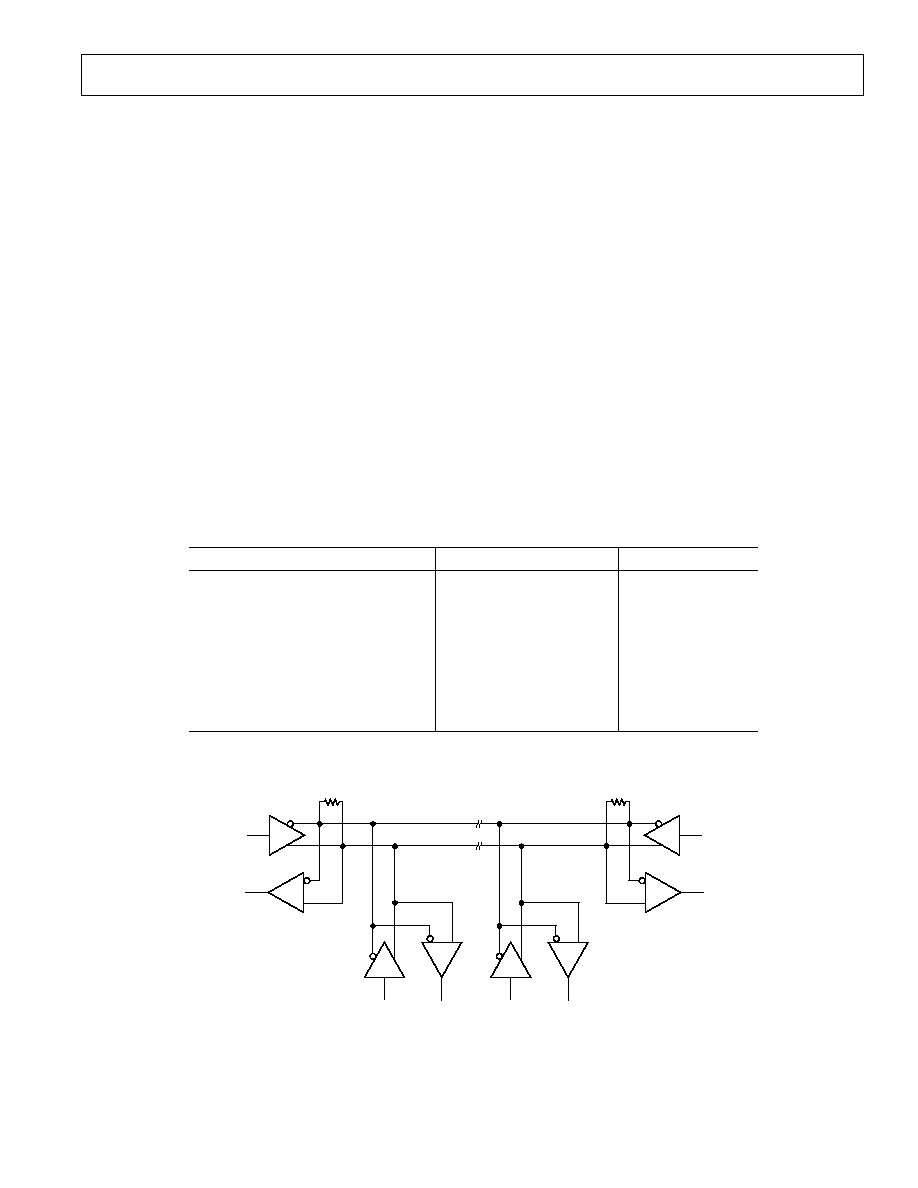
A typical application for the ADM488/ADM489 is illustrated in
Figure 19. This shows a full-duplex link where data may be
transferred at rates up to 250 kbps. A terminating resistor is
shown at both ends of the link. This termination is not critical
since the slew rate is controlled by the ADM488/ADM489 and
reflections are minimized.
The communications network may be extended to include
multipoint connections as shown in Figure 25. Up to 32 trans-
ceivers may be connected to the bus.
Tables I and II show the truth tables for transmitting and
receiving.
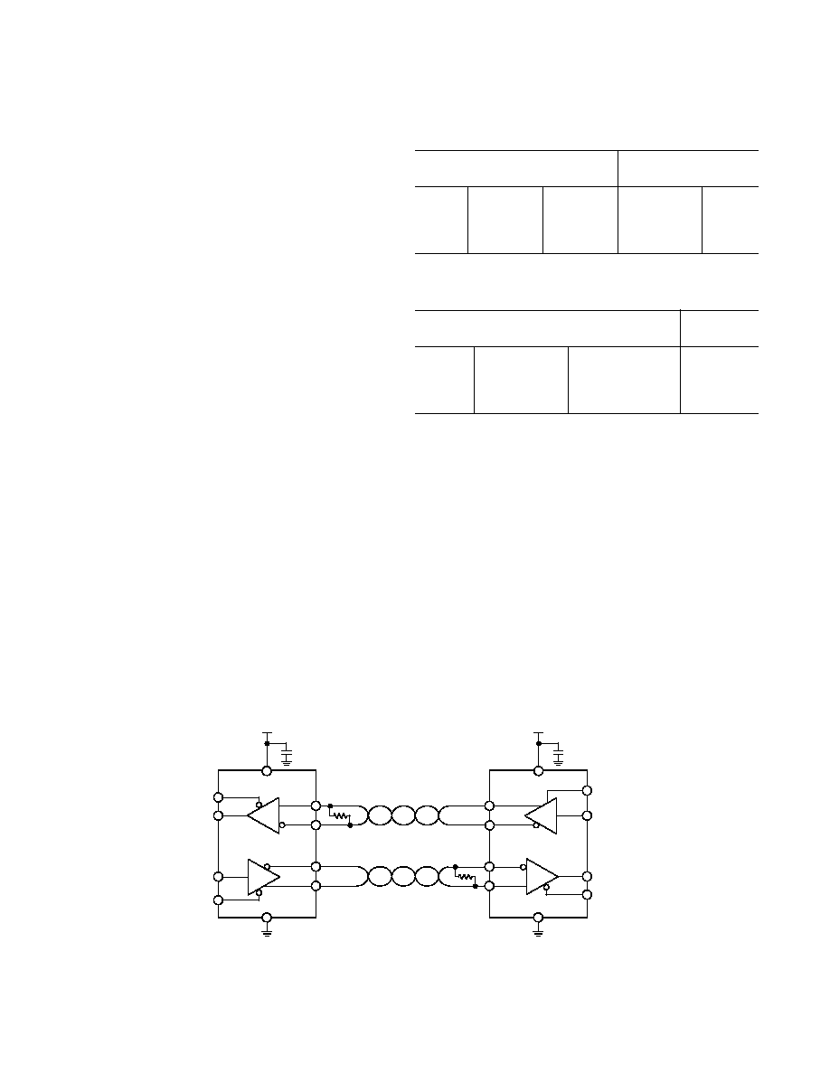
Table I. Transmitting Truth Table
Inputs
Outputs
RE
DE
DI
Z
Y
X
1
1
0
1
X
1
0
1
0
0
0
X
Hi-Z
Hi-Z
1
0
X
Hi-Z
Hi-Z
X = Don't Care.
Table II. Receiving Truth Table
Inputs
Output
RE
DE
A-B
RO
0
0
+0.2 V
1
0
1
+0.2 V
0
0
0
Inputs O/C
1
1
0
X
Hi-Z
X = Don't Care.
EFT TRANSIENT PROTECTION SCHEME
The ADM488/ADM489 uses protective clamping structures on
its inputs and outputs that clamp the voltage to a safe level and
dissipates the energy present in ESD (Electrostatic) and EFT
(Electrical Fast Transients) discharges.
FAST TRANSIENT BURST IMMUNITY (IEC1000-4-4)
IEC1000-4-4 (previously 801-4) covers electrical fast-transient/
burst (EFT) immunity. Electrical fast transients occur as a
result of arcing contacts in switches and relays. The tests simu-
late the interference generated when, for example, a power relay
disconnects an inductive load. A spark is generated due to the
well known back EMF effect. In fact, the spark consists of a
burst of sparks as the relay contacts separate. The voltage ap-
pearing on the line, therefore, consists of a burst of extremely
fast transient impulses. A similar effect occurs when switching
on fluorescent lights.
ADM488
D
RO
DI
A
B
Z
Y
RE
DE
+5V
0.1 F
RS-485/RS-422 LINK
R
R
ADM489
+5V
0.1 F
D
RO
DI
RE
DE
GND
GND
V
CC
V
CC
A
B
Z
Y
Figure 19. ADM488/ADM489 Full-Duplex Data Link
ADM488/ADM489
9
REV. 0
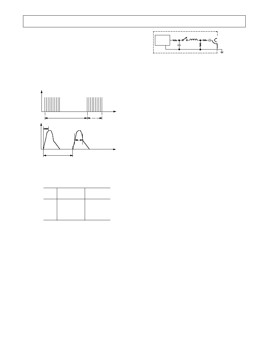
The fast transient burst test, defined in IEC1000-4-4, simulates
this arcing and its waveform is illustrated in Figure 20. It
consists of a burst of 2.5 kHz to 5 kHz transients repeating at
300 ms intervals. It is specified for both power and data lines.
Four severity levels are defined in terms of an open-circuit volt-
age as a function of installation environment. The installation
environments are defined as
1. Well-protected
2. Protected
3. Typical Industrial
4. Severe Industrial
300ms
16ms
V
t
V
0.2/0.4ms
t
5ns
50ns
Figure 20. IEC1000-4-4 Fast Transient Waveform
Table III shows the peak voltages for each of the environments.
Table III.
V
PEAK
(kV)
V
PEAK
(kV)
Level
PSU
I-O
1
0.5
0.25
2
1
0.5
3
2
1
4
4
2
A simplified circuit diagram of the actual EFT generator is
illustrated in Figure 21.
These transients are coupled onto the signal lines using an EFT
coupling clamp. The clamp is 1 m long and completely sur-
rounds the cable, providing maximum coupling capacitance
(50 pF to 200 pF typ) between the clamp and the cable. High
energy transients are capacitively coupled onto the signal lines.
Fast rise times (5 ns) as specified by the standard result in very
effective coupling. This test is very severe since high voltages are
coupled onto the signal lines. The repetitive transients can often
cause problems, where single pulses do not. Destructive latchup
may be induced due to the high energy content of the transients.
Note that this stress is applied while the interface products are
powered up and are transmitting data. The EFT test applies
hundreds of pulses with higher energy than ESD. Worst case
transient current on an I-O line can be as high as 40 A.
HIGH
VOLTAGE
SOURCE
R
C
C
C
Z
S
L
R
M
C
D
50
OUTPUT
Figure 21. EFT Generator
Test results are classified according to the following:
1. Normal performance within specification limits.
2. Temporary degradation or loss of performance that is self-
recoverable.
3. Temporary degradation or loss of function or performance
that requires operator intervention or system reset.
4. Degradation or loss of function that is not recoverable due to
damage.
The ADM488/ADM489 has been tested under worst case con-
ditions using unshielded cables, and meets Classification 2 at
severity Level 4. Data transmission during the transient condi-
tion is corrupted, but it may be resumed immediately following
the EFT event without user intervention.
RADIATED IMMUNITY (IEC1000-4-3)
IEC1000-4-3 (previously IEC801-3) describes the measurement
method and defines the levels of immunity to radiated electro-
magnetic fields. It was originally intended to simulate the elec-
tromagnetic fields generated by portable radio transceivers or
any other device that generates continuous wave radiated electro-
magnetic energy. Its scope has since been broadened to include
spurious EM energy, which can be radiated from fluorescent
lights, thyristor drives, inductive loads, etc.
Testing for immunity involves irradiating the device with an EM
field. There are various methods of achieving this including use
of anechoic chamber, stripline cell, TEM cell and GTEM cell.
These consist essentially of two parallel plates with an electric
field developed between them. The device under test is placed
between the plates and exposed to the electric field. There are
three severity levels having field strengths ranging from 1 V to
10 V/m. Results are classified as follows:
1. Normal Operation.
2. Temporary Degradation or loss of function that is self-
recoverable when the interfering signal is removed.
3. Temporary degradation or loss of function that requires
operator intervention or system reset when the interfering
signal is removed.
4. Degradation or loss of function that is not recoverable due to
damage.
ADM488/ADM489
10
REV. 0
The ADM488/ADM489 comfortably meets Classification 1 at
the most stringent (Level 3) requirement. In fact, field strengths
up to 30 V/m showed no performance degradation and error-
free data transmission continued even during irradiation.
Table IV.
Level
V/m
Field Strength
1
1
2
3
3
10
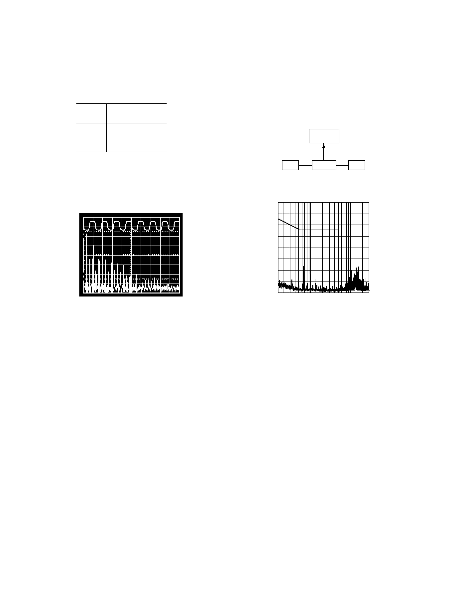
EMI EMISSIONS
The ADM488/ADM489 contains internal slew rate limiting in
order to minimize the level of electromagnetic interference
generated. Figure 22 shows an FFT plot when transmitting a
150 kHz data stream.
10
0%
100
90
10dB/DIV
500kHz/DIV
0
5MHz
Figure 22. Driver Output Waveform and FFT Plot Trans-
mitting @ 150 kHz
As may be seen, the slew limiting attenuates the high frequency
components. EMI is therefore reduced, as are reflections due to
improperly terminated cables.
EN55022, CISPR22 defines the permitted limits of radiated
and conducted interference from Information Technology
Equipment (ITE).
The objective is to control the level of emissions, both con-
ducted and radiated.
For ease of measurement and analysis, conducted emissions are
assumed to predominate below 30 MHz, while radiated emis-
sions predominate above this frequency.
CONDUCTED EMISSIONS
This is a measure of noise that is conducted onto the mains
power supply. The noise is measured using a LISN (Linc Im-
pedance Stabilizing Network) and a spectrum analyzer. The test
setup is illustrated in Figure 23. The spectrum analyzer is set to
scan the spectrum from 0 MHz to 30 MHz. Figure 24 shows
that the level of conducted emissions from the ADM488/
ADM489 are well below the allowable limits.
SPECTRUM
ANALYZER
DUT
LISN
PSU
Figure 23. Conducted Emissions Test Setup
LOG FREQUENCY (0.1530) MHz
0.3
0.6
1
3
6
10
30
80
0
70
40
30
20
10
60
50
LIMIT
dBµV
Figure 24. Conducted Emissions
ADM488/ADM489
11
REV. 0
Table V. Comparison of RS-422 and RS-485 Interface Standards
Specification
RS-422
RS-485
Transmission Type
Differential
Differential
Maximum Data Rate
10 MB/s
10 MB/s
Maximum Cable Length
4000 ft.
4000 ft.
Minimum Driver Output Voltage
±
2 V
±
1.5 V
Driver Load Impedance
100
54
Receiver Input Resistance
4 k
min
12 k
min
Receiver Input Sensitivity
±
200 mV
±
200 mV
Receiver Input Voltage Range
7 V to +7 V
7 V to +12 V
Number of Drivers/Receivers Per Line
1/10
32/32
D
R
D
R
D
D
R
R
RT
RT
Figure 25. Typical RS-485 Network
APPLICATIONS INFORMATION
Differential Data Transmission
Differential data transmission is used to reliably transmit data
at high rates over long distances and through noisy environ-
ments. Differential transmission nullifies the effects of ground
shifts and noise signals, which appear as common-mode volt-
ages on the line. Two main standards are approved by the
Electronics Industries Association (EIA), which specify the
electrical characteristics of transceivers used in differential
data transmission.
The RS-422 standard specifies data rates up to 10 MBaud and
line lengths up to 4000 ft. A single driver can drive a transmis-
sion line with up to 10 receivers.
In order to cater to true multipoint communications, the RS-
485 standard was defined. This standard meets or exceeds all
the requirements of RS-422 and also allows for up to 32 drivers
and 32 receivers to be connected to a single bus. An extended
common-mode range of 7 V to +12 V is defined. The most
significant difference between RS-422 and RS-485 is the fact
that the drivers may be disabled thereby allowing more than
one (32, in fact) to be connected to a single line. Only one
driver should be enabled at a time but the RS-485 standard
contains additional specifications to guarantee device safety in
the event of line contention.
Cable and Data Rate
The transmission line of choice for RS-485 communications is a
twisted pair. Twisted pair cable tends to cancel common mode
noise and also causes cancellation of the magnetic fields gener-
ated by the current flowing through each wire, thereby reducing
the effective inductance of the pair.
The ADM488/ADM489 is designed for bidirectional data com-
munications on multipoint transmission lines. A typical applica-
tion showing a multipoint transmission network is illustrated in
Figure 25. An RS-485 transmission line can have as many as
32 transceivers on the bus. Only one driver can transmit at
a particular time but multiple receivers may simultaneously
be enabled.
As with any transmission line, it is important that reflections are
minimized. This may be achieved by terminating the extreme
ends of the line using resistors equal to the characteristic imped-
ance of the line. Stub lengths of the main line should also be
kept as short as possible. A properly terminated transmission
line appears purely resistive to the driver.

ADM488/ADM489
12
REV. 0
C3160129/97
PRINTED IN U.S.A.
8-Lead Narrow Body (SOIC)
(SO-8)
0.1968 (5.00)
0.1890 (4.80)
8
5
4
1
0.2440 (6.20)
0.2284 (5.80)
PIN 1
0.1574 (4.00)
0.1497 (3.80)
0.0688 (1.75)
0.0532 (1.35)
SEATING
PLANE
0.0098 (0.25)
0.0040 (0.10)
0.0192 (0.49)
0.0138 (0.35)
0.0500
(1.27)
BSC
0.0098 (0.25)
0.0075 (0.19)
0.0500 (1.27)
0.0160 (0.41)
8
°
0
°
0.0196 (0.50)
0.0099 (0.25)
x 45
°
8-Lead Plastic DIP
(N-8)
8
1
4
5
0.430 (10.92)
0.348 (8.84)
0.280 (7.11)
0.240 (6.10)
PIN 1
SEATING
PLANE
0.022 (0.558)
0.014 (0.356)
0.060 (1.52)
0.015 (0.38)
0.210 (5.33)
MAX
0.130
(3.30)
MIN
0.070 (1.77)
0.045 (1.15)
0.100
(2.54)
BSC
0.160 (4.06)
0.115 (2.93)
0.325 (8.25)
0.300 (7.62)
0.015 (0.381)
0.008 (0.204)
0.195 (4.95)
0.115 (2.93)
OUTLINE DIMENSIONS
Dimensions shown in inches and (mm).
14-Lead Plastic DIP
(N-14)
14
1
7
8
0.795 (20.19)
0.725 (18.42)
0.280 (7.11)
0.240 (6.10)
PIN 1
0.325 (8.25)
0.300 (7.62)
0.015 (0.381)
0.008 (0.204)
0.195 (4.95)
0.115 (2.93)
SEATING
PLANE
0.022 (0.558)
0.014 (0.356)
0.060 (1.52)
0.015 (0.38)
0.210 (5.33)
MAX
0.130
(3.30)
MIN
0.070 (1.77)
0.045 (1.15)
0.100
(2.54)
BSC
0.160 (4.06)
0.115 (2.93)
14-Lead Narrow Body (SOIC)
(R-14)
14
8
7
1
0.3444 (8.75)
0.3367 (8.55)
0.2440 (6.20)
0.2284 (5.80)
0.1574 (4.00)
0.1497 (3.80)
PIN 1
SEATING
PLANE
0.0098 (0.25)
0.0040 (0.10)
0.0192 (0.49)
0.0138 (0.35)
0.0688 (1.75)
0.0532 (1.35)
0.0500
(1.27)
BSC
0.0099 (0.25)
0.0075 (0.19)
0.0500 (1.27)
0.0160 (0.41)
8
°
0
°
0.0196 (0.50)
0.0099 (0.25)
x 45
°
16-Lead Thin Shrink Small Outline Package (TSSOP)
(RU-16)
16
9
8
1
0.201 (5.10)
0.193 (4.90)
0.256 (6.50)
0.246 (6.25)
0.177 (4.50)
0.169 (4.30)
PIN 1
SEATING
PLANE
0.006 (0.15)
0.002 (0.05)
0.0118 (0.30)
0.0075 (0.19)
0.0256
(0.65)
BSC
0.0433
(1.10)
MAX
0.0079 (0.20)
0.0035 (0.090)
0.028 (0.70)
0.020 (0.50)
8
°
0
°