 | ÐлекÑÑоннÑй компоненÑ: ADM5170 | СкаÑаÑÑ:  PDF PDF  ZIP ZIP |
Äîêóìåíòàöèÿ è îïèñàíèÿ www.docs.chipfind.ru
ADM5170
REV. 0
One Technology Way, P.O. Box 9106, Norwood. MA 02062-9106, U.S.A.
Tel: 617/329-4700
Fax: 617/326-8703
a
Information furnished by Analog Devices is believed to be accurate and
reliable. However, no responsibility is assumed by Analog Devices for its
use, nor for any infringements of patents or other rights of third parties
which may result from its use. No license is granted by implication or
otherwise under any patent or patent rights of Analog Devices.
Octal, RS-232/RS-423 Line Driver
Truth Table
Inputs
Outputs
EN
Data
EIA RS-232E
1
RS-423A
0
0
(V
DD
3 V)
5 V to 6 V
0
1
(V
SS
3 V)
5 V to 6 V
1
X
High Z
High Z
1
Minimum Output Level
FEATURES
Eight Single Ended Line Drivers in One Package
Meets EIA Standard RS-232E, RS-423A and
CCITT V.10/X.26
Resistor Programmable Slew Rate
Wide Supply Voltage Range
Low Power CMOS
3-State Outputs
TTL/CMOS Compatible Inputs
Output Short Circuit Protection
Available in 28-Pin DIP/PLCC
Low Power Replacement for UC5170C
APPLICATIONS
High Speed Communication
Computer I-O Ports Peripherals
High Speed Modems
Printers
Logic Level Translation
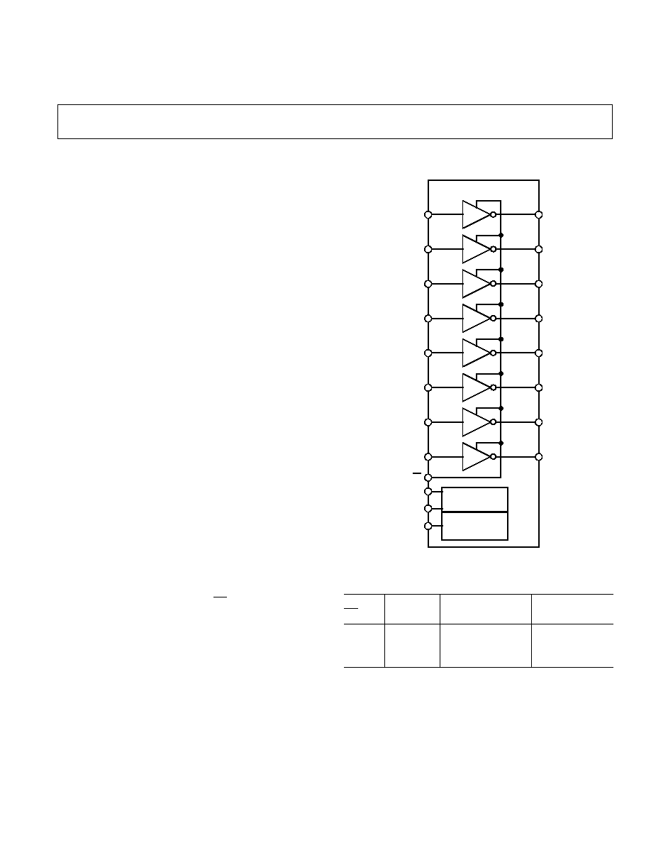
FUNCTIONAL BLOCK DIAGRAM
A
B
C
D
E
F
G
H
A
I
B
I
C
I
D
I
E
I
F
I
G
I
H
I
RS-232/RS-423
MODE SELECT
A
O
B
O
C
O
D
O
E
O
F
O
G
O
H
O
ADM5170
SLEW RATE
CONTROL
EN
MS+
MS
SRA
GENERAL DESCRIPTION
The ADM5170 is an octal line driver suitable for digital communi-
cation systems with data rates up to 116 kB/s. Input TTL or
CMOS signal levels are inverted and translated into either EIA
RS-232E or RS-423A signal levels depending on the status of the
Mode Select inputs MS+ and MS. With both Mode Select inputs
at GND, RS-423 operation is selected while with MS+ connected
to V
DD
and MS connected to V
SS
, RS-232 operation is selected.
The output slew rates may be controlled using an external resistor
connected between the SRA (Slew Rate Adjust) pin and GND.
Resistor values between 2 k
and 10 k
may be selected giving a
slew rate which can be adjusted from 10 V/
µ
s to 2.2 V/
µ
s. This
adjustment of the slew rate allows tailoring of the output character-
istics to suit the interface cable being used.
The outputs may be disabled using the EN (Enable Input). This
feature permits sharing of a common output line.
The ADM5170 is fabricated on an advanced CMOS process
featuring low power consumption. In the disabled state the power
consumption reduces from 500 mW to 40 mW. The ADM5170 is
available in both 28-pin DIP and 28-lead PLCC packages.
Parameter
Min
Typ
Max
Units
Test Conditions/Comments
POWER REQUIREMENTS
V
DD
Range
9
15
V
V
SS
Range
9
15
V
I
DD
(Disabled)
2
4
mA
EN = High,
I
DD
(Enabled)
25
36
mA
R
L
=
, EN = 0 V
I
SS
(Disabled)
2
4
mA
EN = High
I
SS
(Enabled)
23
36
mA
R
L
=
, EN = 0 V
DIGITAL INPUTS
Input Logic Threshold High, V
INH
2.0
V
Input Logic Threshold Low, V
INL
0.8
V
Input Clamp Voltage, V
INK
1.1
1.8
V
I
IN
= 15 mA
Input High Level Current, I
INH
1
µ
A
V
INH
= 2.4 V
Input Low Level Current, I
INL
1
µ
A
V
INL
= 0.4 V
OUTPUTS
RS-423A Outputs
EN = 0.8 V, MS+ = MS = 0 V
High Level Output Voltage
5.0
5.3
6.0
V
R
L
=
, V
IN
= 0.8 V
5.0
5.3
6.0
V
R
L
= 3 k
, V
IN
= 0.8 V
4.5
5.2
6.0
V
R
L
= 450
, V
IN
= 0.8 V
Low Level Output Voltage
5.0
5.3
6.0
V
R
L
=
, V
IN
= 2.0 V
5.0
5.6
6.0
V
R
L
= 3 k
, V
IN
= 2.0 V
4.5
5.4
6.0
V
R
L
= 450
, V
IN
= 2.0 V
Output Balance, V
BAL
0.05
0.4
V
R
L
= 450
, V
BAL
= V
OH
V
OL
RS-232 Outputs
EN = 0.8 V, MS+ = V
DD
, MS = V
SS
High Level Output Voltage
7.0
7.6
V
DD
V
R
L
=
, V
IN
= 0.8 V
7.0
7.6
V
DD
V
R
L
= 3 k
, V
IN
= 0.8 V
Low Level Output Voltage
7.0
7.7
V
SS
V
R
L
=
, V
IN
= 2.0 V
7.0
7.7
V
SS
V
R
L
= 3 k
, V
IN
= 2.0 V
Off-State Output Current, I
OZ
100
100
µ
A
EN = 2.0 V, V
O
=
±
6 V, V
DD
= 15 V, V
SS
= 15 V
Short Circuit Current, I
OS
15
50
100
mA
V
IN
= 0 V, EN = 0 V
15
40
100
mA
V
IN
= 5 V, EN = 0 V
Specifications subject to change without notice.
Parameter
Min
Typ
Max
Units
Test Conditions/Comments
Output Slew Rate
Fig 1, Fig 2. R
SRA
= 2 k
, R
L
= 450
, C
L
= 50 pF
6.65
10
14
V/
µ
s
Rising/Falling Edge, t
R
, t
F
Output Slew Rate
Fig 1, Fig 2. R
SRA
= 10 k
, R
L
= 450
, C
L
= 50 pF
1.33
2.0
3
V/
µ
s
Rising/Falling Edge, t
R
, t
F
Output to Hi-Z Propagation Delay (Disable)
Fig 1, Fig 3. R
SRA
= 10 k
, R
L
= 450
, C
L
= 50 pF
0.3
1.0
µ
s
t
HZ
0.5
1.0
µ
s
t
LZ
Hi-Z to Valid Output Propagation Delay (Enable)
Fig 1, Fig 3. R
SRA
= 10 k
, R
L
= 450
, C
L
= 50 pF
6.0
15
µ
s
t
ZH
7.0
15
µ
s
t
ZL
REV. 0
ADM5170SPECIFICATIONS
2
TIMING CHARACTERISTICS
( V
DD
= +10 V
±
10%, V
SS
= 10 V
±
10%, MS+ = MS = 0 V. All Specifications T
MIN
to T
MAX
unless otherwise noted.)
( V
DD
= +10 V
±
10%, V
SS
= 10 V
±
10% V, MS+ = MS = 0 V, R
SRA
=
10 k
. All Specifications T
MIN
to T
MAX
unless otherwise noted.)
Specifications subject to change without notice.
REV. 0
3
ADM5170
ABSOLUTE MAXIMUM RATINGS*
(T
A
= 25
°
C unless otherwise noted)
V
DD
. . . . . . . . . . . . . . . . . . . . . . . . . . . . . . . . . . . . . . . . . . . +15 V
V
SS
. . . . . . . . . . . . . . . . . . . . . . . . . . . . . . . . . . . . . . . . . . . . . 15 V
Input Voltages
V
IN
. . . . . . . . . . . . . . . . . . . . . . . . . . . . . . . 0.3 to (V
DD
+ 0.3 V)
Ouput Voltages
V
OUT
. . . . . . . . . . . . . . . . . . . . . . . . . . . . . . . . . . 12 V to +12 V
Output Short Circuit Duration . . . . . . . . . . . . . . . . . . Continuous
Power Dissipation Plastic DIP . . . . . . . . . . . . . . . . . . . . 1250 mW
(Derate at 12.5 mW/
°
C above +50
°
C)
JA
, Thermal Impedance . . . . . . . . . . . . . . . . . . . . . . . . . 75
°
C/W
Power Dissipation PLCC . . . . . . . . . . . . . . . . . . . . . . . 1000 mW
(Derate at 10 mW/
°
C above +50
°
C)
JA
, Thermal Impedance . . . . . . . . . . . . . . . . . . . . . . . . . 80
°
C/W
Operating Temperature Range
Commercial (J Version) . . . . . . . . . . . . . . . . . . . . 0
°
C to +70
°
C
Industrial (A Version) . . . . . . . . . . . . . . . . . . . . 40
°
C to +85
°
C
Lead Temperature (Soldering 10 sec) . . . . . . . . . . . . . . . . +300
°
C
Vapour Phase (60 sec) . . . . . . . . . . . . . . . . . . . . . . . . . . +215
°
C
Infrared (15 sec) . . . . . . . . . . . . . . . . . . . . . . . . . . . . . . . +220
°
C
*This is a stress rating only and functional operation of the device at these or any
other conditions above those indicated in the operation sections of this specifica-
tion is not implied. Exposure to absolute maximum rating conditions for extended
periods of time may affect reliability.
ORDERING GUIDE
Model
Temperature Range
Package Option
ADM5170JN
0
°
C to +70
°
C
N-28
ADM5170AN
40
°
C to +85
°
C
N-28
ADM5170JP
0
°
C to +70
°
C
P-28A
ADM5170AP
40
°
C to +85
°
C
P-28A
CAUTION
ESD (electrostatic discharge) sensitive device. Electrostatic charges as high as 4000 V readily
accumulate on the human body and test equipment and can discharge without detection. Although
the ADM5170 features proprietary ESD protection circuitry, permanent damage may occur on
devices subjected to high energy electrostatic discharges. Therefore, proper ESD precautions are
recommended to avoid performance degradation or loss of functionality.
WARNING!
ESD SENSITIVE DEVICE
RS-232/RS-423
MODE SELECT
SLEW RATE
CONTROL
MS+
MS
SRA
EN
V
IN
R
L
C
L
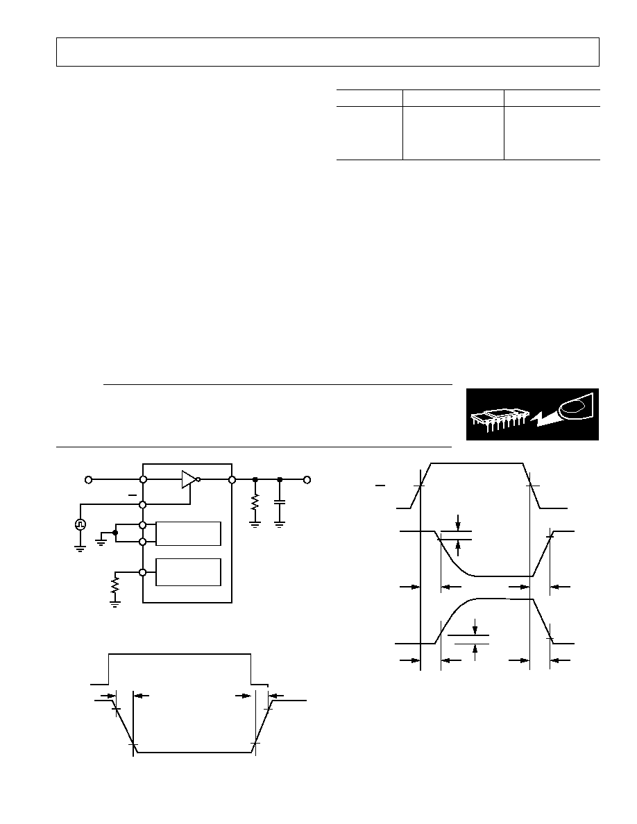
Figure 1. Timing Test Circuit
90%
t
F
10%
90%
10%
t
R
V
IN
V
OUT
Figure 2. Rise/Fall Timing Waveforms
Figure 3. Enable/Disable Timing Waveforms
INPUT
EN
OUTPUT
V
IN
= 0V
t
HZ
0.5V
0.5V
t
LZ
t
ZL
t
ZH
90%
90%
1.5V
1.5V
OUTPUT
V
IN
= 5V
V
OL
V
OH
Slew Rate Programming
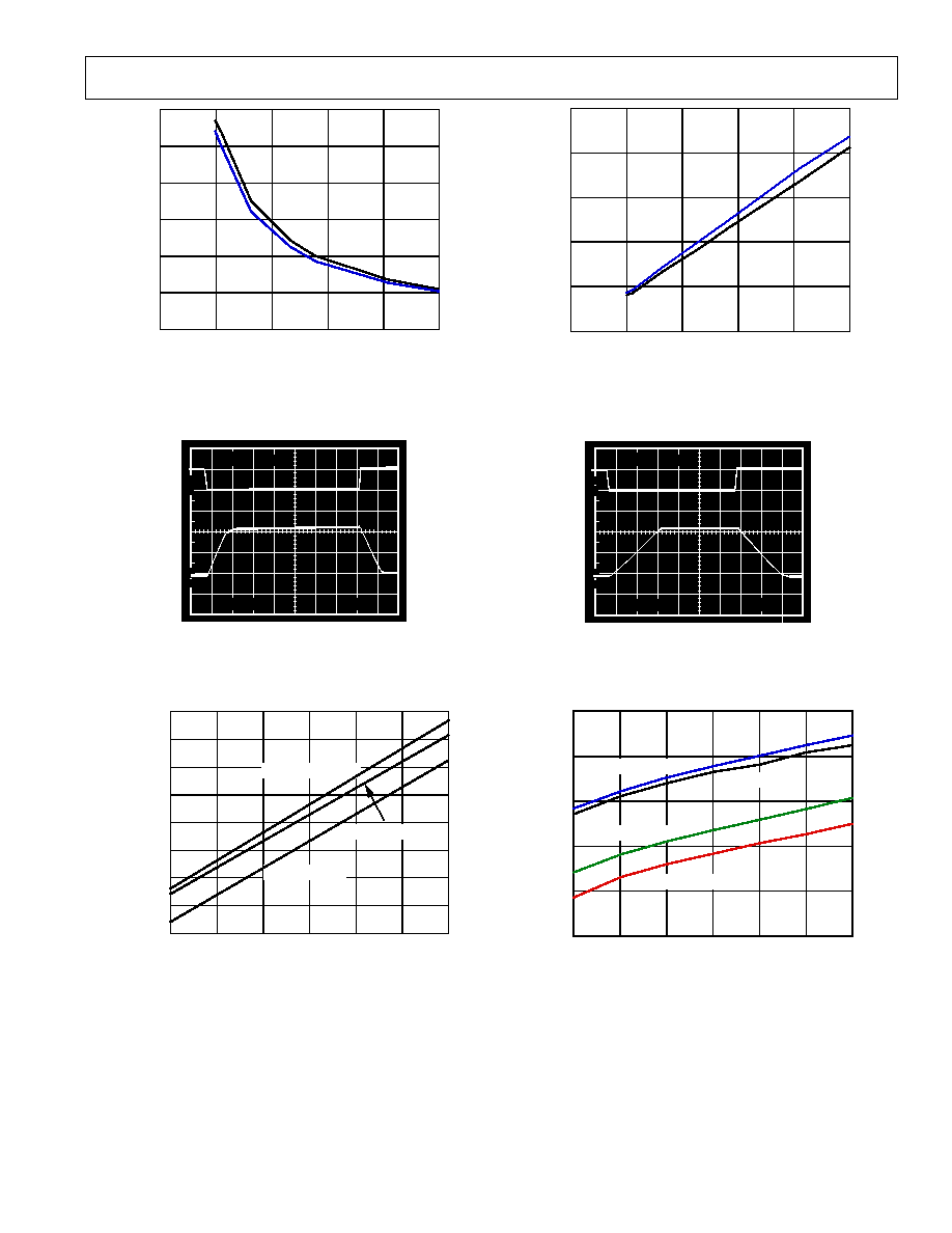
The slew rate for the ADM5170 is controlled by a single resistor
connected between the SRA pin and GND. The slew rate is
approximately.
Slew Rate (V/
µ
s) = 20/R
SRA
(k
)
Resistors between 2 k
and 10 k
may be used providing a slew
rate which may be varied from 10 V/
µ
s to 2.2 V/
µ
s. Figure 5 in the
Typical Performance Characteristics section shows how the slew
rate varies with R
SRA
while Figure 8 shows how the transition time
(10% to 90%) varies with R
SRA
. Waveshaping of the output allows
the user to control the level of interference (near-end crosstalk)
which may be coupled to adjacent circuits in an interconnection.
The recommended output characteristics for cable length and data
rate are given in the EIA RS-423A specifications.
Maximum Data Rate (kB/s) = 300/t (for rates from 1 kB/s to
100 kB/s).
Cable Length (feet) = 100 X t (Max Length = 4000 ft.)
where t is the transition time (in
µ
s) for the output to swing from
10% to 90% of its steady state values. The absolute maximum data
rate is 100 kB/s and the maximum cable length is limited to 4000 ft.
Output Mode Programming
The ADM5170 has two programmable output modes which
provide different output voltage levels. The low output mode meets
the specifications of EIA standards RS-423A while the high output
mode meets the RS-232 specifications. The high output mode
provides greater output swings and is suitable for driving lines
where higher attenuation levels must be tolerated. This mode is
selected by connecting the mode select pins to the supplies, MS+ to
V
DD
and MS to V
SS
. The low output mode is selected by connect-
ing both mode select pins MS+ and MS to GND. This mode
provides a controlled output swing with lower output levels.
Inputs
Outputs
MS+
MS
EN
Data
Output
GND
GND
0
0
5 V to 6 V (RS-423)
GND
GND
0
1
5 V to 6 V (RS-423)
V
DD
V
SS
0
0
(V
DD
3 V) (RS-232)
1
V
DD
V
SS
0
1
(V
SS
+ 3 V) (RS-232)
1
X
X
1
X
High Z
1
Minimum Output Level.
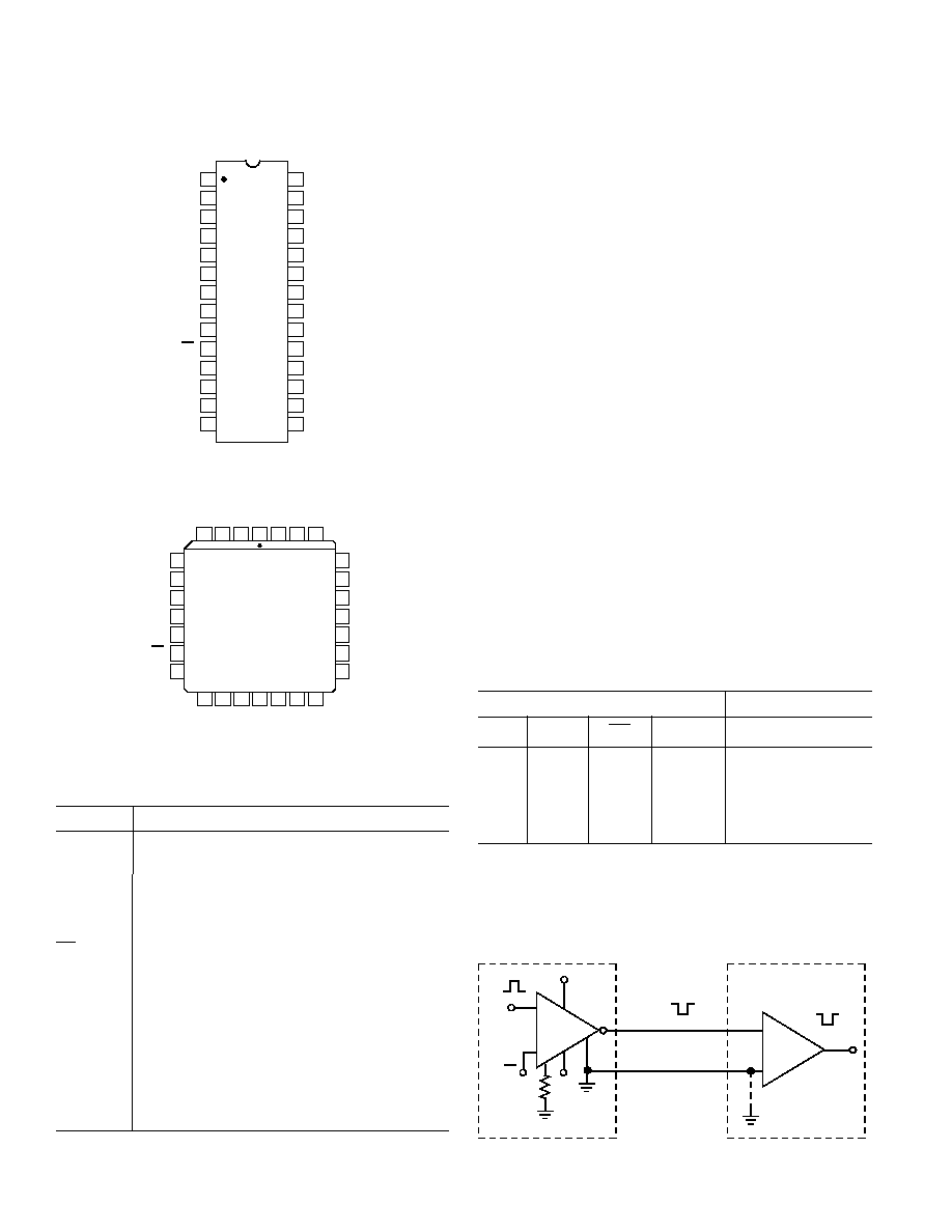
Typical Application Circuit
A typical application circuit using a single driver in the ADM5170
is shown in Figure 4. This circuit is suitable for either RS-232 or
RS-423 communication. An ADM5180 octal receiver is used to
translate the signal back to CMOS logic level at the receiving end.
V
L
V
H
1/8
ADM5170
EN
V
SS
V
DD
TIE TO GND
FOR RS-232
INPUT
RS-232/RS-422A
TRANSMISSION
+V
V
R
SL
1/8
ADM5180
V
L
V
H
PIN FUNCTION DESCRIPTION
Mnemonic
Function
V
DD
Power Supply Input, +10 V
±
10%.
V
SS
Power Supply Input, 10 V
±
10%.
GND
Ground Pin. Must be connected to 0 V.
A
I
. . . H
I
Digital Input to Drivers A to H.
A
O
. . . H
O
RS-232/RS-423 Output from Drivers A to H.
EN
Enable Pin. When high, all outputs are 3-stated.
MS+, MS
Mode Select Inputs. Used to control the output
level swing. With MS+ & MS connected to GND,
RS-423A output levels are selected. With MS+
connected to V
DD
and MS connected to V
SS
,
RS-232 output levels are developed.
SRA
Slew Rate Adjust Input. An external resistor (2 k
to 10 k
) connected between this pin and GND is
used to control the Output Slew Rate (10 V/
µ
s to
2.2 V/
µ
s).
REV. 0
4
ADM5170
PIN CONFIGURATIONS
DIP
GND
NC = NO CONNECT
NC
A
O
H
O
H
I
B
O
C
O
C
I
F
O
F
I
E
I
A
I
B
I
G
I
G
O
D
I
E
O
D
O
V
DD
EN
MS+
V
SS
SRA
MS
NC
NC
NC
NC
13
18
1
2
28
27
5
6
7
24
23
22
3
4
26
25
8
21
9
20
10
19
11
12
17
16
14
15
TOP VIEW
(Not to Scale)
ADM5170
PLCC
NC = NO CONNECT
G
O
F
O
E
O
V
DD
MS+
F
I
E
I
B
O
C
O
D
O
EN
V
SS
C
I
D
I
B
I
A
I
H
O
H
I
G
I
A
O
SRA
NC
NC
MS
GND
NC
NC
NC
26
27
28
4
2
3
15 18
17
16
12
14
13
25
24
21
20
19
23
22
TOP VIEW
(Not to Scale)
1
5
6
9
10
11
7
8
ADM5170
Figure 4. RS-232/RS-423A Typical Application Circuit
5
Typical Performance CharacteristicsADM5170
Figure 8. Typical Rise/Fall Times (RS-423A Mode) vs.
R
SRA
Figure 5. Typical Slew Rate vs. R
SRA
5
0
10
3
1
2
2
0
4
8
6
4
R
SRA
k
TRANSITION TIME
µ
s
t
r
t
f
12
0
10
6
2
2
4
0
10
8
8
6
4
R
SRA
k
SLEW RATE V/µ
s
t
r
t
f
10
90
100
0%
5V
A1
1
µ
s
20V
5V
Figure 9. Slew Rate (R
SRA
= 10 k
)
Figure 6. Slew Rate (R
SRA
= 2 k
)
V
DD
/
V
SS
V
DRIVER OUTPUT VOLTAGE V
15
7
15
9
8
10
9
11
10
12
13
14
14
13
12
11
V
OL
(R
L
=
3k
)
V
OH/
V
OL
(R
L
=
)
V
OH
(R
L
=
3k
)
Figure 10. V
OH
/V
OL
vs. V
DD
/V
SS
(RS-423 Mode)
Figure 7. V
OH
/V
OL
vs. V
DD
/V
SS
(RS-232 Mode)
V
DD
/
V
SS
V
DRIVER OUTPUT VOLTAGE V
5.6
5.1
15
5.4
5.2
10
5.3
9
5.5
14
13
12
11
V
OH
(R
L
= 450
)
V
OH
(R
L
=
)
V
OL
(R
L
= 450
)
V
OL
(R
L
=
)
REV. 0
10
90
100
0%
5V
A1
1
µ
s
20V
5V
6
ADM5170
10
0
25
6
2
5
4
0
8
20
15
10
OUTPUT CURRENT
mA
DRIVER OUTPUT VOLTAGE
V
V
OH
V
OL
6
0
25
3
1
5
2
0
5
4
20
15
10
OUTPUT CURRENT
mA
DRIVER OUTPUT VOLTAGE
V
V
OH
V
OL
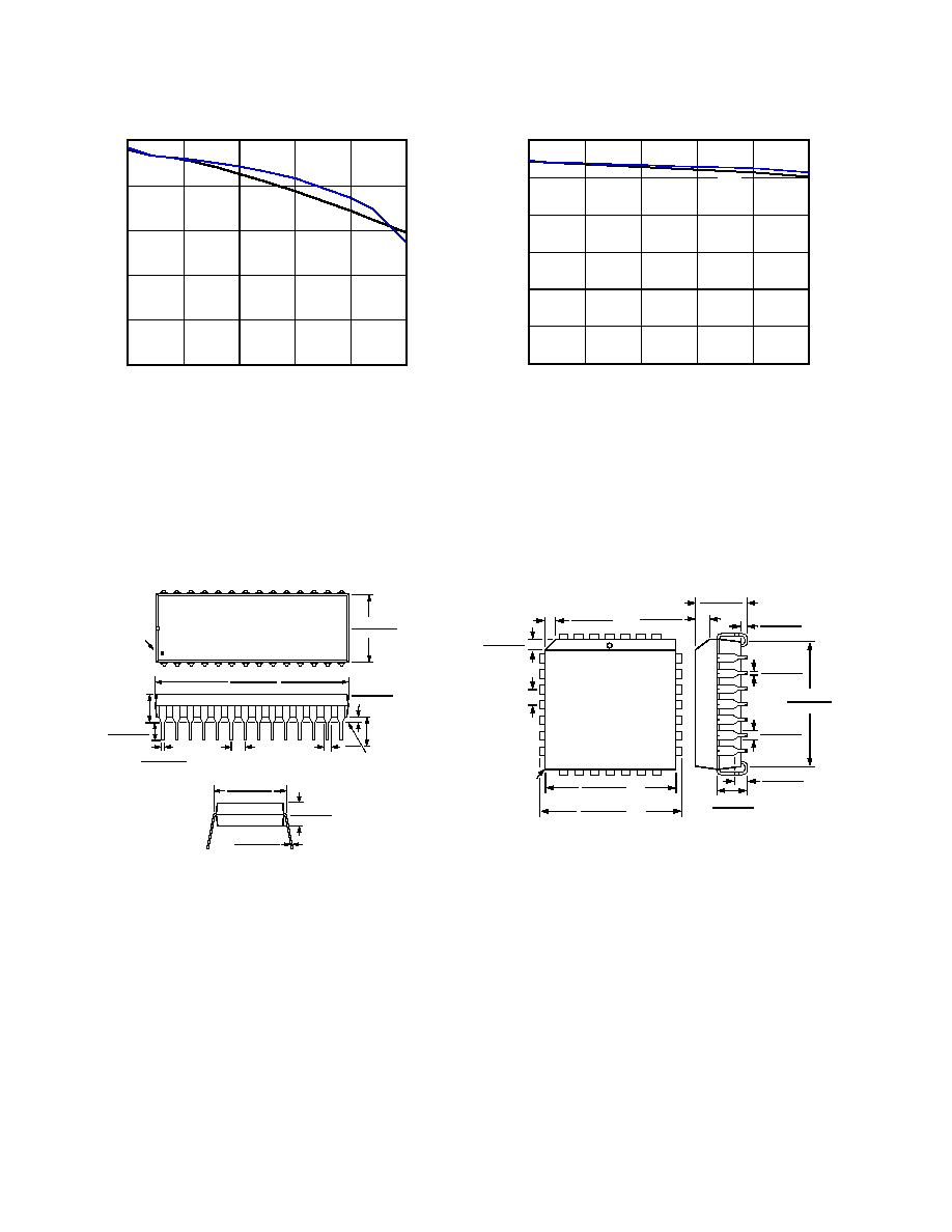
Figure 11. Driver Output Voltage vs. Output Current
(RS-232 Mode)
Figure 12. Driver Output Voltage vs. Output Current
(RS-423 Mode)
PIN
1
0.580 (14.73)
0.485 (12.32)
1
14
15
28
0.625 (15.87)
0.600 (15.24)
0.015 (0.381)
0.008 (0.204)
0.195 (4.95)
0.125 (3.18)
0.250
(6.35)
MAX
0.022 (0.558)
0.014 (0.356)
0.100
(2.54)
BSC
0.200 (5.05)
0.125 (3.18)
0.070 (1.77)
MAX
0.060 (1.52)
0.015 (0.38)
0.150
(3.81)
MIN
SEATING
PLANE
1.565 (39.70)
1.380 (35.10)
OUTLINE DIMENSIONS
Dimensions shown in inches and (mm).
28-Lead Plastic DIP
28-Lead Plastic Leaded Chip Carrier (PLCC)
(N Suffix)
(P Suffix)
0.048 (1.21)
0.042 (1.07)
0.456 (11.58)
0.450 (11.43)
SQ
0.495 (12.57)
0.485 (12.32)
SQ
0.048 (1.21)
0.042 (1.07)
0.050
(1.27)
BSC
26
4
TOP VIEW
25
19
12
11
PIN 1
IDENTIFIER
5
18
0.020
(0.50)
R
0.032 (0.81)
0.026 (0.66)
0.021 (0.53)
0.013 (0.33)
0.056 (1.42)
0.042 (1.07)
0.025 (0.63)
0.015 (0.38)
0.180 (4.57)
0.165 (4.19)
0.430 (10.92)
0.390 (9.91)
0.110 (2.79)
0.085 (2.16)
0.040 (1.01)
0.025 (0.64)
REV. 0
C18537.510/93
PRINTED IN U.S.A.