 | ÐлекÑÑоннÑй компоненÑ: ADM561 | СкаÑаÑÑ:  PDF PDF  ZIP ZIP |
Äîêóìåíòàöèÿ è îïèñàíèÿ www.docs.chipfind.ru
One Technology Way, P.O. Box 9106, Norwood. MA 02062-9106, U.S.A.
Tel: 617/329-4700
Fax: 617/326-8703
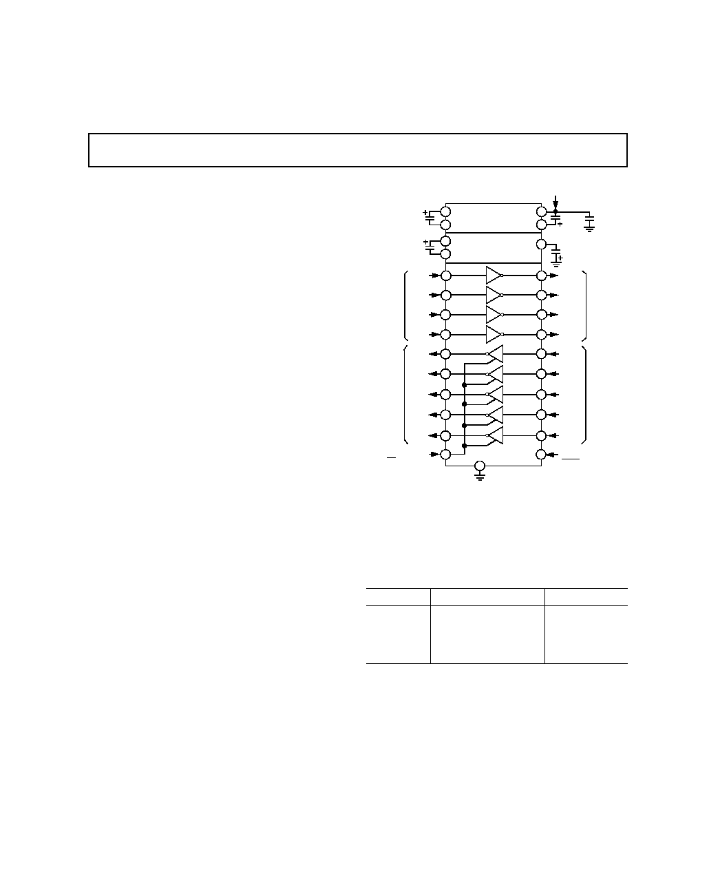
FUNCTIONAL BLOCK DIAGRAM
REV. 0
Information furnished by Analog Devices is believed to be accurate and
reliable. However, no responsibility is assumed by Analog Devices for its
use, nor for any infringements of patents or other rights of third parties
which may result from its use. No license is granted by implication or
otherwise under any patent or patent rights of Analog Devices.
a
Ultralow Power, +3.3 V, RS-232
Notebook PC Serial Port Drivers/Receivers
ADM560/ADM561
FEATURES
RS-232 Compatible
Operates with 3 V or 5 V Logic
Ultralow Power CMOS: 1.3 mA Operation
Low Power Shutdown: 0.2
µ
A
Suitable for Serial Port Mice
116 kbits/s Data Rate
1
µ
F Charge Pump Capacitors
Single +3 V to +3.6 V Power Supply
Two Receivers Active in Shutdown (ADM560)
APPLICATIONS
Laptop Computers
Palmtop Computers
Notebook Computers
Peripherals
Modems
Printers
Battery Operated Equipment
GENERAL DESCRIPTION
The ADM560/ADM561 are four driver/five receiver interface
devices designed to meet the EIA-232 standard while operating
with a single +3.3 V power supply. The devices feature an on-
board dc-to-dc converter, eliminating the need for dual
±
5 V
power supplies. This dc-dc converter contains a voltage doubler
and voltage inverter which internally generates
±
6.6 V from the
input +3.3 V power supply.
The ADM560 and ADM561 consume only 5 mW making
them ideally suited for battery and other power-sensitive appli-
cations. A shutdown facility is also provided which reduces the
power to 0.66
µ
W.
The ADM560 contains active low shutdown and active high
receiver enable signals. In shutdown mode, two receivers remain
active thereby allowing monitoring of peripheral devices. This
feature allows the device to be shut down until a peripheral
device begins communication. The active receivers can alert the
processor which can then take the ADM560 out of the shut-
down mode.
The ADM561 features active high shutdown and an active
low receiver enable. In this device all receivers are disabled in
shutdown.
The ADM560/ADM561 is fabricated using CMOS technology
for minimal power consumption. It features a high level of over-
voltage protection and latch-up immunity. The receiver inputs
ADM560
ADM561
GND
10
SHDN (ADM561)
SHDN
(ADM560)
25
CMOS
OUTPUTS
24
R5
IN
R5
OUT
R5
18
19
R4
IN
R4
OUT
R4
23
22
R1
IN
R1
OUT
R1
R3
IN
R3
OUT
R3
27
26
9
R2
IN
R2
OUT
R2
4
5
8
T1
IN
EIA/TIA-232
OUTPUTS
CMOS
INPUTS
T1
OUT
T3
IN
T3
OUT
T3
20
7
2
1
T1
+3.3V TO +6.6V
VOLTAGE
DOUBLER
+6.6V TO 6.6V
VOLTAGE
INVERTER
16
15
14
12
17
1
µ
F
10V
13
1
µ
F
6.3V
+3.3V INPUT
V
CC
V+
V
C1+
C1
C2+
C2
1
µ
F
10V
1
µ
F
10V
T4
IN
T4
OUT
T4
21
28
11
0.1
µ
F
T2
IN
T2
OUT
6
3
T2
EIA/TIA-232
INPUTS
EN (ADM560)
EN
(ADM561)
can withstand up to
±
25 V levels. The transmitter inputs can be
driven from either 3 V or 5 V logic levels. This allows operation
in mixed 3 V/5 V power supply systems.
The ADM560/ADM561 is packaged in a 28-pin SO and a
28-pin SSOP package.
ORDERING GUIDE
Model
Temperature Range
Package Option
ADM560JR
0
°
C to +70
°
C
R-28
ADM560JRS
0
°
C to +70
°
C
RS-28
ADM561JR
0
°
C to +70
°
C
R-28
ADM561JRS
0
°
C to +70
°
C
RS-28
Parameter
Min
Typ
Max
Units
Test Conditions/Comments
Output Voltage Swing
±
5.0
±
5.5
Volts
V
CC
= 3.3 V, Three Transmitter Outputs
Loaded with 3 k
to Ground
±
4
±
4.5
Volts
V
CC
= 3.0 V, All Transmitter Outputs
Loaded into 3 k
to Ground
V
CC
Power Supply Current
1.3
2
mA
No Load, T
IN
= V
CC
2.2
3.0
mA
No Load,T
IN
= GND
Shutdown Supply Current
0.2
5
µ
A
SHDN
= GND (ADM560); SHDN
= V
CC
(ADM561), T
IN
= V
CC
Input Logic Threshold Low, V
INL
0.4
V
T
IN,
EN, EN, SHDN, SHDN,
Input Logic Threshold High, V
INH
2.4
V
T
IN,
EN, EN, SHDN, SHDN
Logic Pullup Current
3
20
µ
A
T
IN
= GND
EIA-232 Input Voltage Range
25
+25
V
EIA-232 Input Threshold Low
0.4
0.8
V
EIA-232 Input Threshold High
1.1
2.4
V
EIA-232 Input Hysteresis
0.3
V
EIA-232 Input Resistance
3
5
7
k
CMOS Output Voltage Low, V
OL
0.4
V
I
OUT
= 1.6 mA
CMOS Output Voltage High, V
OH
2.8
V
I
OUT
= 40
µ
A
CMOS Output Leakage Current
0.05
±
5
µ
A
EN
= V
CC
, EN = GND, 0 V
R
OUT
V
CC
Output Enable Time
200
ns
Output Disable Time
300
ns
Receiver Propagation Delay
TPHL
0.4
1
µ
s
TPLH
1.3
2
µ
s
Instantaneous Slew Rate
30
V/
µ
s
C
L
= 50 pF, R
L
= 3 k
7 k
Transition Region Slew Rate
5.0
V/
µ
s
R
L
= 3 k
, C
L
= 2500 pF
Measured from +3 V to 3 V or
3 V to +3 V
Transmitter Output Resistance
300
V
CC
= V+ = V = 0 V, V
OUT
=
±
2 V
RS-232 Output Short Circuit Current
±
10
mA
Specifications subject to change without notice.
ADM560/ADM561SPECIFICATIONS
REV. 0
2
(V
CC
= +3.3 V
±
10%, C1C4 = 1
µ
F. All specifications T
MIN
to T
MAX
unless otherwise noted.)
ABSOLUTE MAXIMUM RATINGS*
(T
A
= +25
°
C unless otherwise noted)
V
CC
. . . . . . . . . . . . . . . . . . . . . . . . . . . . . . . . . . 0.3 V to +6 V
V+ . . . . . . . . . . . . . . . . . . . . . . . . . . . . . (V
CC
0.3 V) to +14 V
V . . . . . . . . . . . . . . . . . . . . . . . . . . . . . . . . . . +0.3 V to 14 V
Input Voltages
T
IN
. . . . . . . . . . . . . . . . . . . . . . . . . 0.3 V to (V+, +0.3 V)
R
IN
. . . . . . . . . . . . . . . . . . . . . . . . . . . . . . . . . . . . . . . .
±
25 V
Output Voltages
T
OUT
. . . . . . . . . . . . . . . . . . . (V+, +0.3 V) to (V, 0.3 V)
R
OUT
. . . . . . . . . . . . . . . . . . . . . . . . 0.3 V to (V
CC
+0.3 V)
Short Circuit Duration
T
OUT
. . . . . . . . . . . . . . . . . . . . . . . . . . . . . . . . . Continuous
Power Dissipation
SSOP . . . . . . . . . . . . . . . . . . . . . . . . . . . . . . . . . . . . 900 mW
SOIC . . . . . . . . . . . . . . . . . . . . . . . . . . . . . . . . . . . . 900 mW
Operating Temperature Range
Commercial (J Version) . . . . . . . . . . . . . . . . . .0
°
C to +70
°
C
Storage Temperature Range . . . . . . . . . . . . . 65
°
C to +150
°
C
Lead Temperature (Soldering, 10 sec). . . . . . . . . . . . . +300
°
C
ESD Rating . . . . . . . . . . . . . . . . . . . . . . . . . . . . . . . . . >2000 V
*This is a stress rating only and functional operation of the device at these or any
other conditions above those indicated in the operation sections of this specifica-
tion is not implied. Exposure to absolute maximum rating conditions for extended
periods of time may affect reliability.
ADM560/ADM561
REV. 0
3
Table I.
ADM560
ADM561
SHDN
= 1
SHDN = 0
Normal Operation
EN = 1 Receivers Active
EN
= 0; Receivers Active
EN = 0 Receivers Inactive
EN
= 1; Receivers Inactive
SHDN
= 0
SHDN = 1
Shutdown Mode
EN = 1 Receivers R1R3 Inactive
EN
= 0; Receivers Inactive
EN = 1 Receivers R4 & R5 Active
EN
= 1; Receivers Inactive
EN = 0 Receivers R1R5 Inactive
PIN FUNCTION DESCRIPTION
Mnemonic
Function
V
CC
Power Supply Input 3.3 V
±
10%.
V+
Internally Generated Positive Supply (+6.6 V
Nominal).
V
Internally Generated Negative Supply (6.6 V
Nominal).
GND
Ground Pin. Must Be Connected to 0 V.
C1+, C1
External Capacitor 1 Is Connected Between
These Pins.
C2+, C2
External Capacitor 2 Is Connected Between
These Pins.
T
IN
Transmitter (Driver) Inputs. These Inputs
Accept 3 V or 5 V Logic Levels. An Internal
400 k
Pull-Up Resistor to V
CC
Is Connected
On Each Input.
T
OUT
Transmitter (Driver) Outputs (Typically
±
6 V).
R
IN
Receiver Inputs. These inputs accept RS-232
Signal Levels. An Internal 5 k
Pull-Down
Resistor to GND Is Connected on Each of
These Inputs.
R
OUT
Receiver Outputs. These are 3 V Logic
Levels.
EN/EN
Receiver Enable (Active High on ADM560);
Active Low on ADM561) Refer to Table I.
SHDN
/SHDN
Shutdown Control (Active Low on ADM560);
(Active High on ADM561) Refer to Table I.
PIN CONFIGURATIONS
1
2
3
7
28
27
26
22
8
9
10
21
20
19
11
12
18
17
4
5
25
24
6
23
TOP VIEW
(Not to Scale)
13
14
16
15
ADM560
ADM561
R2
OUT
R2
IN
R5
IN
T4
IN
R3
IN
T1
OUT
T2
OUT
T3
OUT
T4
OUT
R5
OUT
V+
V
V
CC
C1+
C1
C2+
C2
GND
SHDN
(ADM560)
SHDN (ADM561)
R3
OUT
T3
IN
R4
IN
R4
OUT
R1
IN
R1
OUT
T1
IN
T2
IN
EN (ADM560)
EN
(ADM561)
REV. 0
4
ADM560/ADM561
GENERAL DESCRIPTION
The ADM560/ADM561 are RS-232 transmission line drivers/
receivers which operate from a single +3.3 V supply. This is
achieved by integrating step up voltage converters and level
shifting transmitters and receivers onto the same chip. CMOS
technology is used to keep the power dissipation to an absolute
minimum. The ADM560/ADM561 is a modification, enhance-
ment and improvement to the AD230AD241 family and
derivatives thereof. It is essentially plug-in compatible and does
not have materially different applications.
The ADM560/ADM561 contains an internal voltage doubler
and a voltage inverter which generates
±
6.6 V from the +3.3 V
input. Four external 1
µ
F capacitors are required for the internal
voltage converter.
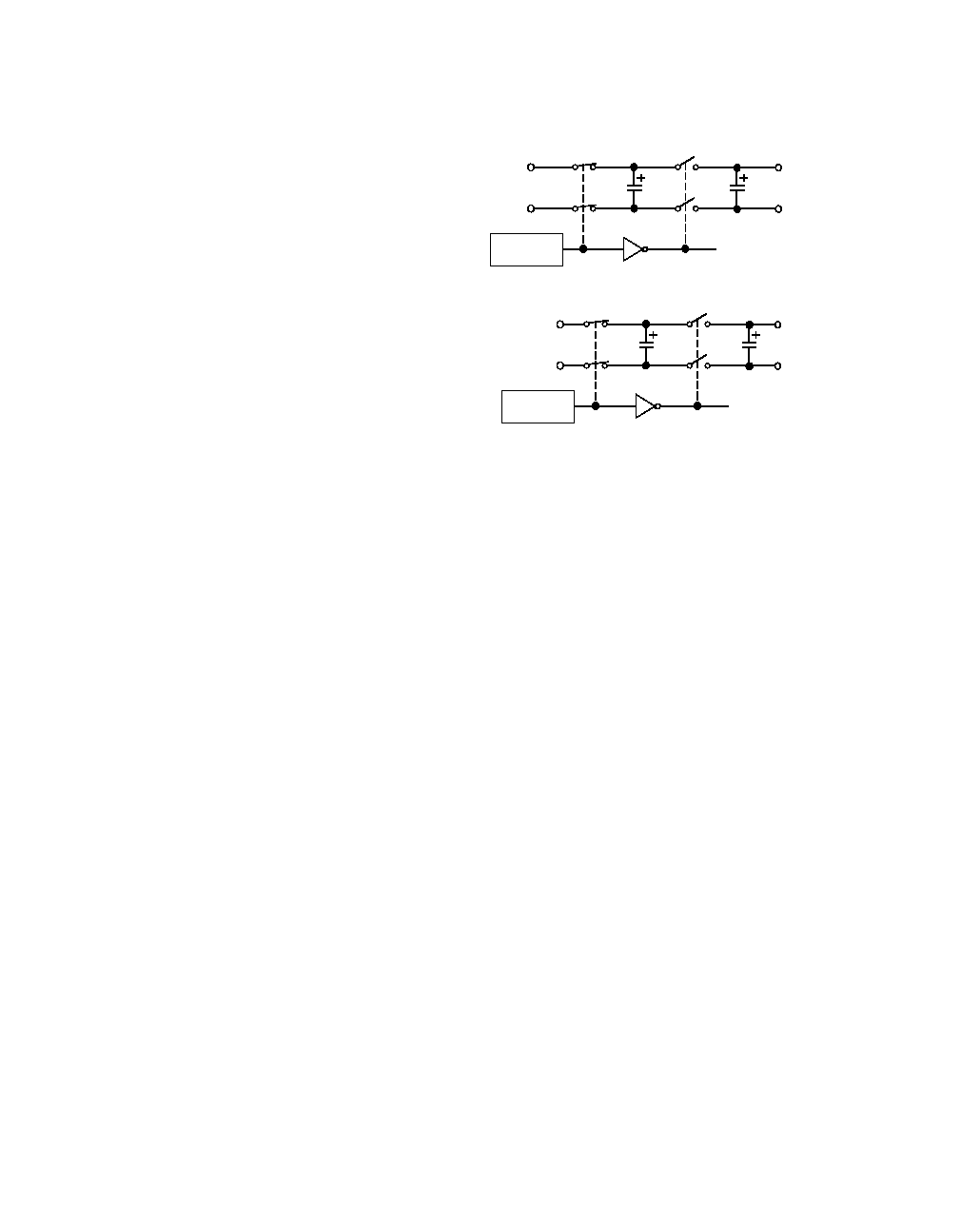
CIRCUIT DESCRIPTION
The internal circuitry consists of three main sections. These
are:
1. A charge pump voltage converter
2. 3 V Logic to EIA-232 transmitters
3. EIA-232 to 3 V Logic receivers.
Charge Pump DC-DC Voltage Converter
The Charge Pump Voltage converter consists of an oscillator
and a switching matrix. The converter generates a
±
6.6 V sup-
ply from the input +3.3 V level. This is done in two stages using
a switched capacitor technique as illustrated below. First, the
3.3 V input supply is doubled to 6.6 V using capacitor C1 as the
charge storage element. The 6.6 V level is then inverted to gen-
erate 6.6 V using C2 as the storage element.
Capacitors C3 and C4 are used to reduce the output ripple.
Their values are not critical and can be reduced if higher levels
of ripple are acceptable. The charge pump capacitors C1 and
C2 may also be reduced at the expense of higher output imped-
ance on the V+ and V supplies.
The V+ and V supplies may also be used to power external
circuitry if the current requirements are small.
Transmitter (Driver) Section
The Drivers convert 3 V or 5 V logic input levels into EIA-232
output levels. With V
CC
= +3.3 V and driving an EIA-232 load,
the output voltage swing is typically
±
5.5 V.
S1
S3
V+ = 2V
CC
S2
S4
INTERNAL
OSCILLATOR
C1
C3
V
CC
GND
V
CC
Figure 1. Charge Pump Voltage Doubler
S1
S3
S2
S4
INTERNAL
OSCILLATOR
C2
C4
V = (V+)
GND
V+
GND
FROM
VOLTAGE
DOUBLER
Figure 2. Charge Pump Voltage Inverter
Unused inputs may be left unconnected, as an internal 400 k
pull-up resistor pulls them high forcing the outputs into a low
state. The input pull-up resistors typically source 8
µ
A when
grounded so unused inputs should either be connected to V
CC
or left unconnected in order to minimize power consumption.
Receiver Section
The receivers are inverting level shifters which accept EIA-232
input levels and translate them into 3 V logic output levels.
The inputs have internal 5 k
pull-down resistors to ground
and are also protected against overvoltages of up to
±
25 V. The
guaranteed switching thresholds are 0.4 V minimum and 2.4 V
maximum. Unconnected inputs are pulled to 0 V by the internal
5 k
pull-down resistor. This, therefore, results in a Logic 1
output level for unconnected inputs or for inputs connected to
GND.
The receivers have schmitt trigger input with a hysteresis level
of 0.3 V. This ensures error-free reception for both noisy inputs
and for inputs with slow transition times.
ENABLE AND SHUTDOWN
Table I shows the truth table for the enable and shutdown con-
trol signals. When disabled, all receivers are placed in a high
impedance state. In shutdown, all transmitters are disabled and
all receivers on the ADM561 are disabled. On the ADM560,
receivers R4 and R5 remain enabled in shutdown.
ADM560/ADM561
REV. 0
5
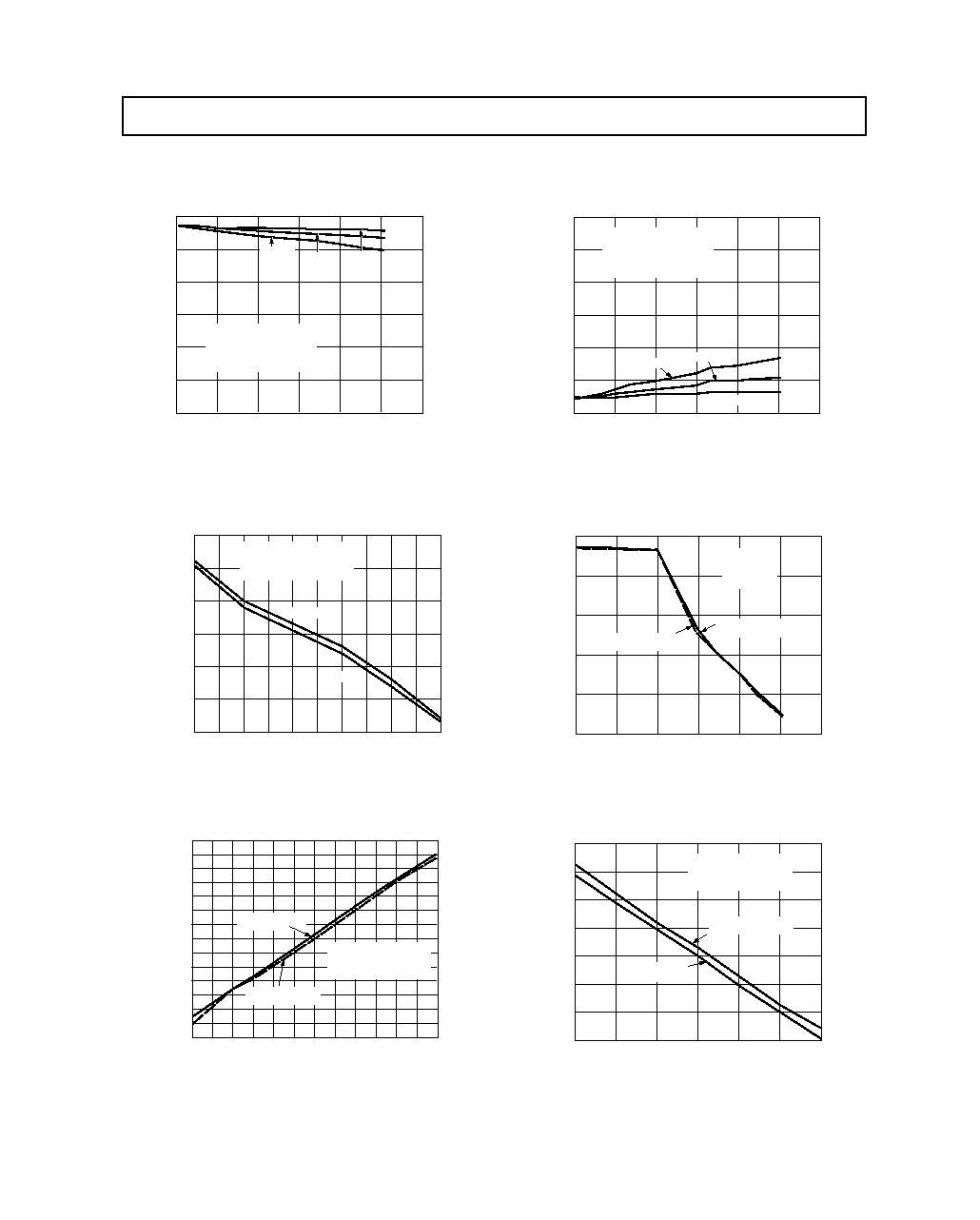
Typical Performance Curves
6
0
3000
3
1
500
2
0
5
4
2500
2000
1500
1000
LOAD CAPACITANCE pF
V
OH
Volts
20kbps
80kbps
160kbps
T
A
= +25
°
C
V
CC
= +3.3V
4 TRANSMITTERS LOADED
WITH RL = 5k
|| CL
C1 C4 = 1µF
Figure 3. Transmitter Output Voltage High vs. Load
Capacitance
6.25
4.75
5
5.25
0
5.75
3
4
2
1
| I
OUT
| mA
| T
OUT
| Volts
T
A
= +25
°
C
C1 C4 = 1µF
V
CC
= +3.3V
TRANSMITTERS UNLOADED
T
OUT
HIGH
T
OUT
LOW
Figure 4. Transmitter Output Voltage vs. Load Current
10.5
3.5
5.5
5.5
2.5
7.5
6.5
8.5
9.5
5.0
4.5
4.0
3.5
3.0
4.5
V
CC
Volts
V
OH
Volts
1 TRANSMITTER
LOADED
4 TRANSMITTERS
LOADED
T
A
= +25
°
C
C1 C4 = 1µF
TRANSMITTERS LOADED
WITH 5k
|| 2500pF
Figure 5. Transmitter Output Voltage High vs. V
CC
0
6
3000
3
5
500
4
0
1
2
2500
2000
1500
1000
LOAD CAPACITANCE pF
V
OL
Volts
160kbps
80kbps
20kbps
T
A
= +25
°
C
V
CC
= +3.3V
4 TRANSMITTERS LOADED
WITH RL = 5k
|| C
L
C1 C4 = 1µF
Figure 6. Transmitter Output Voltage Low vs. Load
Capacitance
7.5
2.5
3000
5.5
3.5
500
4.5
0
6.5
2500
2000
1500
1000
LOAD CAPACITANCE pF
SLEW RATE V/µs
T
A
= +25
°
C
V
CC
= +3.3V
R
L
= 5k
C1 C4 = 1µF
3 TRANSMITTERS
LOADED
4 TRANSMITTERS
LOADED
Figure 7. Transmitter Slew Rate vs. Load Capacitance
3
10
5.5
7
9
3.0
8
2.5
4
6
5
5.0
4.5
4.0
3.5
V
CC
Volts
V
OL
Volts
T
A
= +25
°
C
C1 C4 = 1µF
TRANSMITTERS LOADED
WITH 5k
|| 2500pF
4 TRANSMITTERS
LOADED
1 TRANSMITTER
LOADED
Figure 8. Transmitter Output Voltage Low vs. V
CC
REV. 0
6
ADM560/ADM561
PRINTED IN U.S.A.
C194057/94
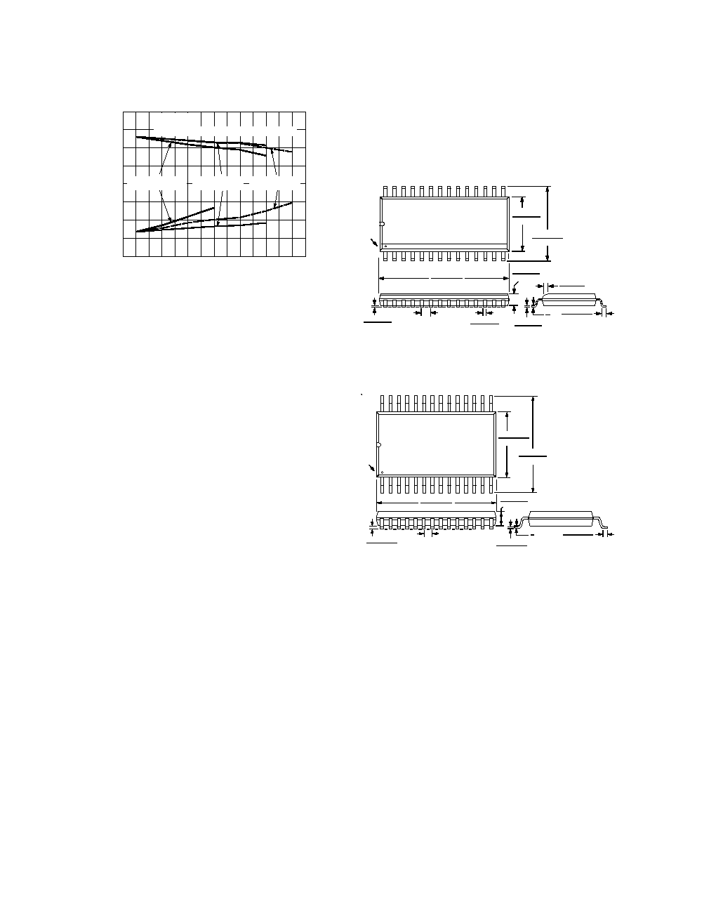
OUTLINE DIMENSIONS
Dimensions shown in inches and (mm).
28-Lead SO
(R-28)
0.019 (0.49)
0.014 (0.35)
0.05 (1.27)
BSC
0.708 (18.02)
0.696 (17.67)
0.01 (0.254)
0.006 (0.15)
0.096 (2.44)
0.089 (2.26)
0.013 (0.32)
0.009 (0.23)
0.042 (1.067)
0.018 (0.457)
6
°
0
°
0.03 (0.76)
0.02 (0.51)
PIN 1
0.299 (7.6)
0.291 (7.39)
0.414 (10.52)
0.398 (10.10)
15
14
1
28
1. LEAD NO. IDENTIFIED BY A DOT.
28-Lead SSOP
(RS-28)
1. LEAD NO. 1 IDENTIFIED BY A DOT.
2 LEADS WILL BE EITHER TIN PLATED OR SOLDER DIPPED
0.009 (0.229)
0.005 (0.127)
0.037 (0.94)
0.022 (0.559)
8
°
0
°
0.0256 (0.65)
BSC
0.407 (10.34)
0.397 (10.08)
0.008 (0.203)
0.002 (0.050)
0.07 (1.78)
0.066 (1.67)
PIN 1
15
14
1
28
0.311 (7.9)
0.301 (7.64)
0.212 (5.38)
0.205 (5.207)
10
10
5
0
0
5
20
15
13
10
5
25
CURRENT mA
OUTPUT VOLTAGE V+, V Volts
V+ AND V
EQUALLY LOADED
V+ LOADED
NO LOAD ON V
V LOADED
NO LOAD ON V+
T
A
= +25
°
C
V
CC
= 3.3V
C1 C4 = 1µF ALL TRANSMITTERS UNLOADED
Figure 9. V+, V vs. Load Current