Document Outline
- Specifications
- Pinout
- Package drawings
- Ordering Guide
- Features
- Applications
- Product Description
- Absolute Maximum Ratings
- Functional Block Diagram
- Pin Function Description
- Circuit Description
- Typical Characteristics
- APPLICATIONS
- Diagrams
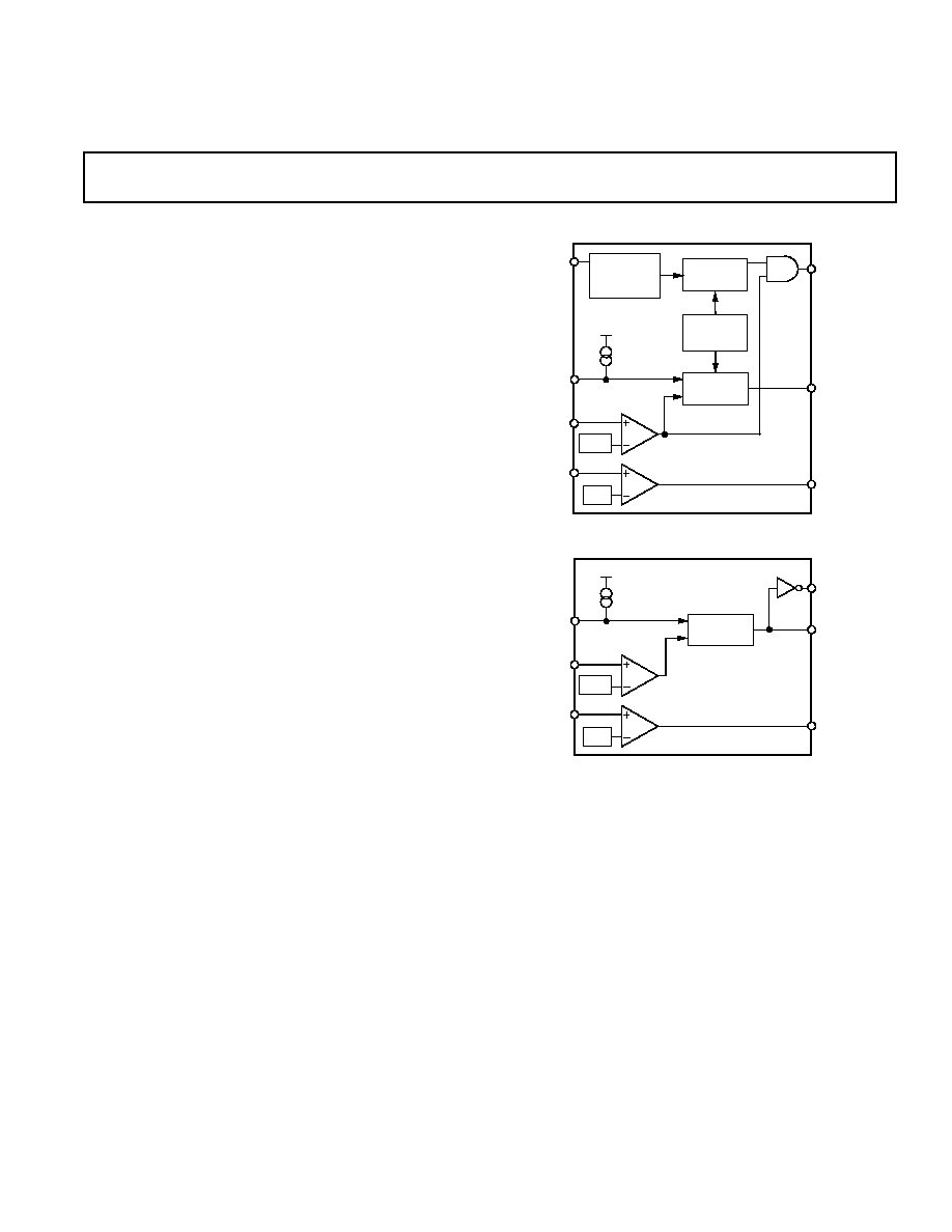
- ADM706 Functional Block Diagram
- ADM708 Functional Block Diagram
- RESET , MR and WDO Timing
- Watchdog Timing
- Power-Fail Comparator
- Adding Hysteresis to the Power-Fail Comparator
- RESET Valid Below 1 V
- Typical Application Circuit
- RESET from WDO
- Monitoring 3 V/3.3 V and an Additional Supply, VX
- Bidirectional I-O RESET
FUNCTIONAL BLOCK DIAGRAMS
REV. A
Information furnished by Analog Devices is believed to be accurate and
reliable. However, no responsibility is assumed by Analog Devices for its
use, nor for any infringements of patents or other rights of third parties
which may result from its use. No license is granted by implication or
otherwise under any patent or patent rights of Analog Devices.
a
+3 V, Voltage Monitoring
P Supervisory Circuits
FEATURES
Precision Supply-Voltage Monitor
+2.63 V (ADM706P/R, ADM708R)
+2.93 V (ADM706S, ADM708S)
+3.08 V (ADM706T, ADM708T)
100 A Quiescent Current
200 ms Reset Pulsewidth
Debounced Manual Reset Input (
MR)
Independent Watchdog Timer--1.6 sec Timeout
(ADM706x)
Reset Output
Active High (ADM706P)
Active Low (ADM706R/S/T)
Both Active High and Active Low (ADM708R/S/T)
Voltage Monitor for Power-Fail or Low Battery Warning
Guaranteed
RESET Valid with V
CC
= 1 V
Superior Upgrade for MAX706P/R/S/T, MAX708R/S/T
APPLICATIONS
Microprocessor Systems
Computers
Controllers
Intelligent Instruments
Critical P Monitoring
Automotive Systems
Battery Operated Systems
Portable Instruments
GENERAL DESCRIPTION
The ADM706P/R/S/T and the ADM708R/S/T microprocessor
supervisory circuits are suitable for monitoring either 3 V or 3.3 V
power supplies.
The ADM706P/R/S/T provide the following functions:
1. Power-supply monitoring circuitry which generates a Reset
output during power-up, power-down and brownout condi-
tions. The reset output remains operational with V
CC
as low
as 1 V.
2. Independent watchdog monitoring circuitry which is acti-
vated if the watchdog input has not been toggled within
1.6 seconds.
3. A 1.25 V threshold detector for power fail warning, low bat-
tery detection, or to monitor an additional power supply.
4. An active low debounced manual reset input (
MR).
The ADM706R, ADM706S, ADM706T are identical except for
the reset threshold monitor levels which are 2.63 V, 2.93 V, and
3.08 V respectively. The ADM706P is identical to the ADM706R
in that the reset threshold is 2.63 V. It differs only in that it has
an active high reset output.
ADM706P/R/S/T, ADM708R/S/T
The ADM708R/S/T provide the same functionality as the
ADM706R/S/T and only differ in that:
1.
A watchdog timer function is not available.
2.
An active high reset output (RESET) in addition to the
active low (
RESET) output is available.
All parts are available in 8-lead DIP and narrow SOIC packages.
One Technology Way, P.O. Box 9106, Norwood, MA 02062-9106, U.S.A.
Tel: 781/329-4700
World Wide Web Site: http://www.analog.com
Fax: 781/326-8703
� Analog Devices, Inc., 1999
WATCHDOG
TRANSITION
DETECTOR
WATCHDOG
TIMER
1.25V
V
REF
*
WATCHDOG
INPUT (WDI)
POWER FAIL
INPUT (PFI)
POWER FAIL
OUTPUT (
PFO
)
WATCHDOG
OUTPUT(
WDO
)
RESET
,
(P = RESET)
*
VOLTAGE REFERENCE = 2.63V (P/R), 2.93V (S), 3.08V (T)
ADM706
RESET &
WATCHDOG
TIMEBASE
RESET
GENERATOR
MR
V
CC
70 A
V
CC
1.25V
V
REF
*
POWER FAIL
INPUT (PFI)
POWER FAIL
OUTPUT (
PFO
)
RESET
*
VOLTAGE REFERENCE = 2.63V (R), 2.93V (S), 3.08V (T)
ADM708
RESET
GENERATOR
MR
V
CC
70 A
V
CC
RESET

Parameter
Min
Typ
Max
Units
Test Conditions/Comments
V
CC
Operating Voltage Range
1.0
5.5
V
Supply Current
100
200
�
A
V
CC
< 3.6 V
150
350
�
A
V
CC
< 5.5 V
Reset Threshold (V
RST
)
2.55
2.63
2.70
V
ADM70_P/R
2.85
2.93
3.00
V
ADM70_S
3.00
3.08
3.15
V
ADM70_T
Reset Threshold Hysteresis
20
mV
Reset Pulsewidth
160
200
280
ms
ADM70_P/R, V
CC
= 3 V
160
200
280
ms
ADM70_S/T, V
CC
= 3.3 V
200
ms
V
CC
= 5.0 V
RESET Output Voltage
ADM70_R/S/T
V
OH
0.8
�
V
CC
V
V
RST
(max) < V
CC
< 3.6 V, I
SOURCE
= 500
�
A
V
OL
0.3
V
V
RST
(max) < V
CC
< 3.6 V, I
SINK
= 1.2 mA
V
OH
V
CC
�1.5 V
V
4.5 V < V
CC
< 5.5 V, I
SOURCE
= 800
�
A
V
OL
0.4
V
4.5 V < V
CC
< 5.5 V, I
SINK
= 3.2 mA
V
OL
0.3
V
V
CC
= 1 V, I
SINK
= 100
�
A
RESET Output Voltage
ADM706P
V
OH
V
CC
�0.6 V
V
V
RST
(max) < V
CC
< 3.6 V, I
SOURCE
= 215
�
A
V
OL
0.3
V
V
RST
(max) < V
CC
< 3.6 V, I
SINK
= 1.2 mA
V
OH
V
CC
�1.5 V
V
4.5 V < V
CC
< 5.5 V, I
SOURCE
= 800
�
A
V
OL
0.4
V
4.5 V < V
CC
< 5.5 V, I
SINK
= 3.2 mA
RESET Output Voltage
ADM708_
V
OH
0.8
�
V
CC
V
V
RST
(max) < V
CC
< 3.6 V, I
SOURCE
= 500
�
A
V
OL
0.3
V
V
RST
(max) < V
CC
< 3.6 V, I
SINK
= 500
�
A
V
OH
V
CC
�1.5 V
V
4.5 V < V
CC
< 5.5 V, I
SOURCE
= 800
�
A
V
OL
0.4
V
4.5 V < V
CC
< 5.5 V, I
SINK
= 1.2 mA
Watchdog Timeout Period
1.00
1.60
2.25
sec
ADM70_P/R; V
CC
= 3 V. ADM70_S/T,
V
CC
= 3.3 V
WDI Pulsewidth
V
IL
= 0.4 V, V
IH
= (V
CC
)
�
(0.8)
100
ns
V
RST
(max) < V
CC
< 3.6 V
50
ns
4.5 V < V
CC
< 5.5 V
WDI Input Threshold
ADM706_
V
IL
0.6
V
V
RST
(max) < V
CC
< 3.6 V
V
IH
0.7
�
V
CC
V
V
RST
(max) < V
CC
< 3.6 V
V
IL
0.8
V
V
CC
= 5.0 V
V
IH
3.5
V
V
CC
= 5.0 V
WDI Input Current
�1.0
0.02
1.0
�
A
WDI = 0 V or V
CC
WDO Output Voltage
V
OH
0.8
�
V
CC
V
V
RST
(max) < V
CC
< 3.6 V, I
SOURCE
= 500
�
A
V
OL
0.3
V
V
RST
(max) < V
CC
< 3.6 V, I
SINK
= 500
�
A
V
OH
V
CC
�1.5 V
V
4.5 V < V
CC
< 5.5 V, I
SOURCE
= 800
�
A
V
OL
0.4
V
4.5 V < V
CC
< 5.5 V, I
SINK
= 1.2 mA
MR Pull Up Current
MR = 0 V
25
70
250
�
A
V
RST
(max) < V
CC
< 3.6 V
100
250
600
�
A
4.5 V < V
CC
< 5.5 V
MR Pulsewidth
500
ns
V
RST
(max) < V
CC
< 3.6 V
150
ns
4.5 V < V
CC
< 5.5 V
MR Input Threshold
V
IL
0.6
V
V
RST
(max) < V
CC
< 3.6 V
V
IH
0.7
�
V
CC
V
V
RST
(max) < V
CC
< 3.6 V
V
IL
0.8
V
4.5 V < V
CC
< 5.5 V
V
IH
2.0
V
4.5 V < V
CC
< 5.5 V
ADM706P/R/S/T, ADM708R/S/T�SPECIFICATIONS
REV. A
�2�
(V
CC
= 2.70 V to 5.5 V (ADM70_P/R),
V
CC
= 3.00 V to 5.5 V (ADM70_S), V
CC
= 3.15 V to 5.5 V (ADM70_T), T
A
= T
MIN
to T
MAX
unless otherwise noted.)
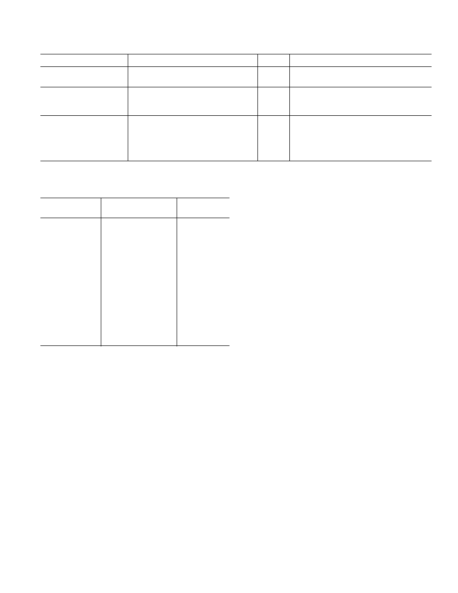
ORDERING GUIDE
Temperature
Package
Model
Range
Options
ADM706PAN
�40
�
C to +85
�
C
N-8
ADM706PAR
�40
�
C to +85
�
C
SO-8
ADM706RAN
�40
�
C to +85
�
C
N-8
ADM706RAR
�40
�
C to +85
�
C
SO-8
ADM706SAN
�40
�
C to +85
�
C
N-8
ADM706SAR
�40
�
C to +85
�
C
SO-8
ADM706TAN
�40
�
C to +85
�
C
N-8
ADM706TAR
�40
�
C to +85
�
C
SO-8
ADM708RAN
�40
�
C to +85
�
C
N-8
ADM708RAR
�40
�
C to +85
�
C
SO-8
ADM708SAN
�40
�
C to +85
�
C
N-8
ADM708SAR
�40
�
C to +85
�
C
SO-8
ADM708TAN
�40
�
C to +85
�
C
N-8
ADM708TAR
�40
�
C to +85
�
C
SO-8
Parameter
Min
Typ
Max
Units
Test Conditions/Comments
MR to Reset Output Delay
750
ns
V
RST
(max) < V
CC
< 3.6 V
250
ns
4.5 V < V
CC
< 5.5 V
PFI Input Threshold
1.2
1.25
1.3
V
ADM70_P/R; V
CC
= 3 V. ADM70_S/T,
V
CC
= 3.3 V, PFI falling
PFI Input Current
�25
0.01
25
nA
PFO Output Voltage
V
OH
0.8
�
V
CC
V
V
RST
(max) < V
CC
< 3.6 V, I
SOURCE
= 500
�
A
V
OL
0.3
V
V
RST
(max) < V
CC
< 3.6 V, I
SINK
= 1.2 mA
V
OH
V
CC
�1.5 V
V
4.5 V < V
CC
< 5.5 V, I
SOURCE
= 800
�
A
V
OL
0.4
V
4.5 V < V
CC
< 5.5 V, I
SINK
= 3.2 mA
ADM706P/R/S/T, ADM708R/S/T
ABSOLUTE MAXIMUM RATINGS*
(T
A
= +25
�
C unless otherwise noted)
V
CC
. . . . . . . . . . . . . . . . . . . . . . . . . . . . . . . . . . �0.3 V to +6 V
All Other Inputs . . . . . . . . . . . . . . . . . . �0.3 V to V
CC
+ 0.3 V
Input Current
V
CC
. . . . . . . . . . . . . . . . . . . . . . . . . . . . . . . . . . . . . . . . 20 mA
GND . . . . . . . . . . . . . . . . . . . . . . . . . . . . . . . . . . . . . . . 20 mA
Digital Output Current . . . . . . . . . . . . . . . . . . . . . . . . . 20 mA
Power Dissipation, N-8 DIP . . . . . . . . . . . . . . . . . . . . 727 mW
JA
Thermal Impedance . . . . . . . . . . . . . . . . . . . . . 135
�
C/W
Power Dissipation, SO-8 SOIC . . . . . . . . . . . . . . . . . . 470 mW
JA
Thermal Impedance . . . . . . . . . . . . . . . . . . . . . 110
�
C/W
Operating Temperature Range
Industrial (A Version) . . . . . . . . . . . . . . . . . �40
�
C to +85
�
C
Lead Temperature (Soldering, 10 secs) . . . . . . . . . . . . +300
�
C
Vapor Phase (60 secs) . . . . . . . . . . . . . . . . . . . . . . . +215
�
C
Infrared (15 secs) . . . . . . . . . . . . . . . . . . . . . . . . . . . +220
�
C
Storage Temperature Range . . . . . . . . . . . . . �65
�
C to +150
�
C
ESD Rating . . . . . . . . . . . . . . . . . . . . . . . . . . . . . . . . . . .>5 kV
*Stresses above those listed under Absolute Maximum Ratings may cause perma-
nent damage to the device. This is a stress rating only; functional operation of the
device at these or any other conditions above those listed in the operational
sections of this specification is not implied. Exposure to absolute maximum
ratings for extended periods of time may affect device reliability.
REV. A
�3�
REV. A
�4�
ADM706P/R/S/T, ADM708R/S/T
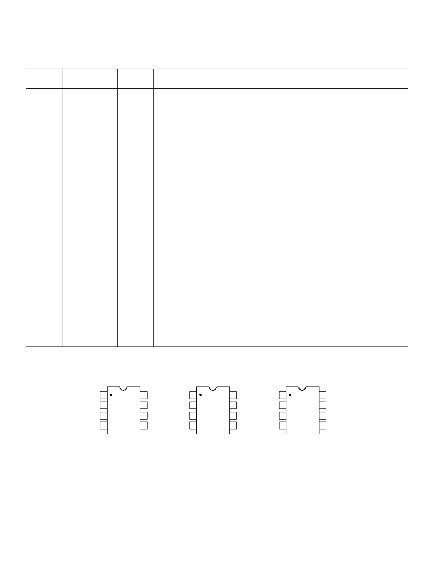
PIN FUNCTION DESCRIPTIONS
Pin No.
Pin No.
Mnemonic
ADM706
ADM708
Function
MR
1
1
Manual Reset Input. When taken below 0.6 V a RESET is generated.
MR can be
driven from TTL, CMOS logic or from a manual reset switch as it is internally
debounced. An internal 70
�
A pull-up current holds the input high when floating.
V
CC
2
2
Power Supply Input.
GND
3
3
0 V. Ground reference for all signals.
PFI
4
4
Power Fail Input. PFI is the noninverting input to the Power Fail Comparator.
When PFI is less than 1.25 V, PFO goes low. If unused, PFI should be connected
to GND.
PFO
5
5
Power Fail Output.
PFO is the output from the Power Fail Comparator. It goes
low when PFI is less than 1.25 V.
WDI
6
N/A
Watchdog Input. WDI is a three level input. If WDI remains either high or low
for longer than the watchdog timeout period, the watchdog output
WDO goes
low. The timer resets with each transition at the WDI input. Either a high-to-low
or a low-to-high transition will clear the counter. The internal timer is also
cleared whenever reset is asserted. The Watchdog Timer is disabled when WDI is
left floating or connected to a three-state buffer.
NC
N/A
6
No Connect.
RESET
7 (R/S/T Only)
7
Logic Output.
RESET goes low for 200 ms when triggered. It can be triggered
either by V
CC
being below the reset threshold or by a low signal on the manual
reset (
MR) input. RESET will remain low whenever V
CC
is below the reset
threshold. It remains low for 200 ms after V
CC
goes above the reset threshold or
MR goes from low to high. A watchdog timeout will not trigger RESET unless
WDO is connected to MR.
RESET
7 (P Only)
8
Logic Output. RESET is an active high output suitable for systems which use
active high RESET logic. It is the inverse of
RESET.
WDO
8
N/A
Logic Output. The Watchdog Output,
WDO, goes low if the internal watchdog
timer times out as a result of inactivity on the WDI input. It remains low until
the watchdog timer is cleared.
WDO also goes low during low line conditions.
Whenever V
CC
is below the reset threshold,
WDO remains low. As soon as V
CC
goes above the reset threshold,
WDO goes high immediately.
PIN CONFIGURATIONS
MR
V
CC
GND
PFI
WDO
RESET
WDI
PFO
1
2
3
4
8
7
6
5
TOP VIEW
(Not to Scale)
ADM706
P
MR
V
CC
GND
PFI
NC = NO CONNECT
RESET
RESET
NC
PFO
1
2
3
4
8
7
6
5
TOP VIEW
(Not to Scale)
ADM708
R/S/T
MR
V
CC
GND
PFI
WDO
RESET
WDI
PFO
1
2
3
4
8
7
6
5
TOP VIEW
(Not to Scale)
ADM706
R/S/T

REV. A
�5�
ADM706P/R/S/T, ADM708R/S/T
WATCHDOG
TRANSITION
DETECTOR
WATCHDOG
TIMER
1.25V
V
REF
*
WATCHDOG
INPUT (WDI)
POWER FAIL
INPUT (PFI)
POWER FAIL
OUTPUT (
PFO
)
WATCHDOG
OUTPUT(
WDO
)
RESET
,
(P = RESET)
*
VOLTAGE REFERENCE = 2.63V (P/R), 2.93V (S), 3.08V (T)
ADM706
RESET &
WATCHDOG
TIMEBASE
RESET
GENERATOR
MR
V
CC
70 A
V
CC
Figure 1. ADM706 Functional Block Diagram
1.25V
V
REF
*
POWER FAIL
INPUT (PFI)
POWER FAIL
OUTPUT (
PFO
)
RESET
*
VOLTAGE REFERENCE = 2.63V (R), 2.93V (S), 3.08V (T)
ADM708
RESET
GENERATOR
MR
V
CC
70 A
V
CC
RESET
Figure 2. ADM708 Functional Block Diagram
CIRCUIT INFORMATION
Power Fail Reset
The reset output provides a reset (
RESET or RESET) output
signal to the Microprocessor whenever the V
CC
input is below
the reset threshold. The actual reset threshold voltage is depen-
dent on whether a P/R, S, or T suffix device is used. An internal
timer holds the reset output active for 200 ms after the voltage
on V
CC
rises above the threshold. This is intended as a power-on
reset signal for the microprocessor. It allows time for both the
power supply and the microprocessor to stabilize after power-
up. If a power supply brownout or interruption occurs, the reset
line is similarly activated and remains active for 200 ms after the
supply recovers. If another interruption occurs during an active
reset period, then the reset timeout period continues for an ad-
ditional 200 ms.
The reset output is guaranteed to remain valid with V
CC
as low
as 1 V. This ensures that the microprocessor is held in a stable
shutdown condition as the power supply starts up.
The ADM706P provides an active high reset (RESET) signal;
the ADM706R/S/T provides an active low (
RESET) signal;
while the ADM708R/S/T provides both RESET and
RESET.
Manual Reset
The manual reset input (
MR) allows other reset sources such as
a manual reset switch to generate a processor reset. The input is
effectively debounced by the timeout period (200 ms typical).
The
MR input is TTL/CMOS compatible so it may also be
driven by any logic reset output. If unused, the
MR input may
be tied high or left floating.
V
CC
RESET
MR
WDO
VRT
VRT
t
RS
t
RS
MR
EXTERNALLY
DRIVEN LOW
NOTE: RESET = COMPLEMENT OF
RESET
Figure 3.
RESET, MR and WDO Timing
Watchdog Timer (ADM706)
The watchdog timer circuit may be used to monitor the activity
of the microprocessor in order to check that it is not stalled in
an indefinite loop. An output line on the processor is used to
toggle the Watchdog Input (WDI) line. If this line is not toggled
within the timeout period (1.6 sec), the watchdog output
(
WDO) is driven low. The WDO output may be connected to a
nonmaskable interrupt (NMI) on the processor. Therefore, if
the watchdog timer times out, an interrupt is generated. The in-
terrupt service routine should then be used to rectify the
problem.
The watchdog timer is cleared by either a high-to-low or by a
low-to-high transition on WDI. Pulses as narrow as 50 ns are
detected. The timer is also cleared by RESET/
RESET going
active. Therefore the watchdog timeout period begins after reset
goes inactive.
When V
CC
falls below the reset threshold,
WDO is forced low
whether or not the watchdog timer has timed out. Normally
this would generate an interrupt but it is overridden by RESET/
RESET going active.
The watchdog monitor can be deactivated by floating the
Watchdog Input (WDI). The
WDO output can now be used as
a low line output since it will only go low when V
CC
falls below
the reset threshold.
t
WP
t
WD
WDI
WDO
RESET
t
RS
RESET EXTERNALLY
TRIGGERED BY
MR
t
WD
t
WD
Figure 4. Watchdog Timing