 | ÐлекÑÑоннÑй компоненÑ: ADM812SAR | СкаÑаÑÑ:  PDF PDF  ZIP ZIP |
ADM811/ADM812 Data Sheet
REV. 0
Information furnished by Analog Devices is believed to be accurate and
reliable. However, no responsibility is assumed by Analog Devices for its
use, nor for any infringements of patents or other rights of third parties
which may result from its use. No license is granted by implication or
otherwise under any patent or patent rights of Analog Devices.
a
ADM811/ADM812
One Technology Way, P.O. Box 9106, Norwood, MA 02062-9106, U.S.A.
Tel: 781/329-4700
World Wide Web Site: http://www.analog.com
Fax: 781/326-8703
© Analog Devices, Inc., 1999
Microprocessors
Supervisory Circuit in 4-Lead SOT-143
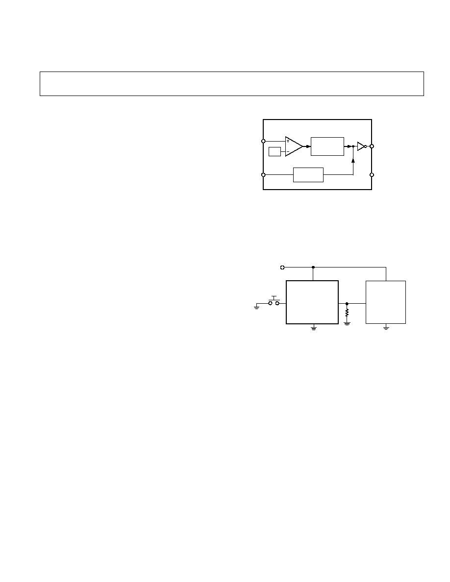
FUNCTIONAL BLOCK DIAGRAM
DEBOUNCE
RESET
/RESET
GND
V
CC
MR
V
REF
ADM811/ADM812
RESET
GENERATOR
FEATURES
Superior Upgrade for MAX811/MAX812
Specified Over Temperature
Low Power Consumption (5 A Typ)
Precision Voltage Monitor: +3 V, +3.3 V, +5 V Options
Reset Assertion Down to 1 V V
CC
140 ms Min Power-On Reset
Logic Low
RESET Output (ADM811)
Logic High RESET Output (ADM812)
Built-In Manual Reset
APPLICATIONS
Microprocessor Systems
Controllers
Intelligent Instruments
Automotive Systems
Safety Systems
Portable Instruments
GENERAL DESCRIPTION
The ADM811/ADM812 are reliable voltage monitoring devices
suitable for use in most voltage monitoring applications.
The ADM811/ADM812 are designed to monitor five different
voltages, each allowing for a 5% or 10% degradation of standard
PSU voltages before a reset occurs. These voltages have been
selected for the effective monitoring of +3 V, +3.3 V and +5 V
supply voltage levels.
Included in this circuit is a debounced Manual Reset input.
Reset can be activated using an electrical switch (or an input
from another digital device) or by a degradation of the supply
voltage. The Manual Reset function is very useful especially if
the circuit in which the ADM811/ADM812 is operating enters
into a state that can only be detected by the user. Allowing the
user to manually reset a system can reduce the damage or dan-
ger that could be otherwise caused by an out-of-control or
locked up system.
V
CC
RESET
RESET
ADM811
V
CC
MR
GND
GND
P
SYSTEM
100k
Figure 1. Typical Operating Circuit

2
REV. 0
ADM811/ADM812SPECIFICATIONS
(V
CC
= Full Operating Range, T
A
= T
MIN
to T
MAX
, V
CC
typ = +5 V
for L/M, +3.3 V for T/S, +3 V for R Models unless otherwise noted)
P
arameter
Min
Typ
Max
Units
Test Conditions/Comments
SUPPLY
Voltage
1.0
5.5
V
T
A
= 0
°
C to +70
°
C
1.2
V
T
A
= 40
°
C to +85
°
C
Current
8
15
µ
A
V
CC
< +5.5 V, ADM81_L/M, I
OUT
= 0 A
5
10
µ
A
V
CC
< +3.6 V, ADM81_R/S/T, I
OUT
= 0 A
RESET VOLTAGE THRESHOLD
ADM81_L
4.54
4.63
4.72
V
T
A
= +25
°
C
ADM81_L
4.50
4.75
V
T
A
= 40
°
C to +85
°
C
ADM81_M
4.30
4.38
4.46
V
T
A
= +25
°
C
ADM81_M
4.25
4.50
V
T
A
= 40
°
C to +85
°
C
ADM81_T
3.03
3.08
3.14
V
T
A
= +25
°
C
ADM81_T
3.00
3.15
V
T
A
= 40
°
C to +85
°
C
ADM81_S
2.88
2.93
2.98
V
T
A
= +25
°
C
ADM81_S
2.85
3.00
V
T
A
= 40
°
C to +85
°
C
ADM81_R
2.58
2.63
2.68
V
T
A
= +25
°
C
ADM81_R
2.55
2.70
V
T
A
= 40
°
C to +85
°
C
RESET THRESHOLD
TEMPERATURE COEFFICIENT
30
ppm/
°
C
V
CC
TO RESET/
RESET DELAY
40
µ
s
V
OD
= 125 mV, ADM81_L/M
20
µ
s
V
OD
= 125 mV, ADM81_R/S/T
RESET ACTIVE TIMEOUT PERIOD
140
560
ms
V
CC
= V
TH(MAX)
300
700
ms
(ADM811-3T Only)
MANUAL RESET
Minimum Pulsewidth
10
µ
s
Glitch Immunity
100
ns
RESET/
RESET Propagation Delay
0.5
µ
s
Pull-Up Resistance
10
20
30
k
The Manual Reset Circuit Will Act On
An Input Rising Above
2.3
V
V
CC
> V
TH(MAX),
ADM81_L/M
An Input Falling Below
0.8
V
V
CC
> V
TH(MAX),
ADM81_L/M
An Input Rising Above
0.7
×
V
CC
V
V
CC
> V
TH(MAX),
ADM81_R/S/T
An Input Falling Below
0.25
×
V
CC
V
V
CC
> V
TH(MAX),
ADM81_R/S/T
RESET Output Voltage
Low (ADM812R/S/T)
0.3
V
V
CC
= V
TH(MAX)
, I
SINK
= 1.2 mA
Low (ADM812L/M)
0.4
V
V
CC
= V
TH(MAX)
, I
SINK
= 3.2 mA
High (ADM812R/S/T/L/M)
0.8 V
CC
V
1.8 V < V
CC
< V
TH(MIN)
, I
SOURCE
= 150
µ
A
Low (ADM811R/S/T)
0.3
V
V
CC
= V
TH(MIN)
, I
SINK
= 1.2 mA
Low (ADM811L/M)
0.4
V
V
CC
= V
TH(MIN)
, I
SINK
= 3.2 mA
Low (ADM811R/S/T/L/M)
0.3
V
V
CC
> 1.0 V, I
SINK
= 50
µ
A
High (ADM811R/S/T)
0.8 V
CC
V
V
CC
> V
TH(MAX)
, I
SOURCE
= 500
µ
A
High (ADM811L/M)
V
CC
1.5
V
V
CC
> V
TH(MAX)
, I
SOURCE
= 800
µ
A
Specifications subject to change without notice.
ABSOLUTE MAXIMUM RATINGS*
(Typical values are at T
A
= +25
°
C unless otherwise noted)
Terminal Voltage (With Respect to Ground)
V
CC
. . . . . . . . . . . . . . . . . . . . . . . . . . . . . . . 0.3 V to +6 V
All Other Inputs . . . . . . . . . . . . . . . . . 0.3 V to V
CC
+ 0.3 V
Input Current
V
CC
. . . . . . . . . . . . . . . . . . . . . . . . . . . . . . . . . . . . . 20 mA
MR . . . . . . . . . . . . . . . . . . . . . . . . . . . . . . . . . . . . . 20 mA
Output Current
RESET, RESET . . . . . . . . . . . . . . . . . . . . . . . . . . . 20 mA
Power Dissipation (T
A
= +70
°
C)
RT-4, SOT-143 . . . . . . . . . . . . . . . . . . . . . . . . . . . 200 mW
Derate by 4 mW/
°
C above +70
°
C
JA
Thermal Impedance . . . . . . . . . . . . . . . . . . . . 330
°
C/W
Operating Temperature Range . . . . . . . . . . . 40
°
C to +85
°
C
Storage Temperature Range . . . . . . . . . . . . 65
°
C to +160
°
C
Lead Temperature (Soldering, 10 sec) . . . . . . . . . . . . +300
°
C
Vapor Phase (60 sec) . . . . . . . . . . . . . . . . . . . . . . . . +215
°
C
Infrared (15 secs) . . . . . . . . . . . . . . . . . . . . . . . . . . . +220
°
C
ESD Rating . . . . . . . . . . . . . . . . . . . . . . . . . . . . . . . . . . . 3 kV
*Stresses above those listed under Absolute Maximum Ratings may cause perma-
nent damage to the device. This is a stress rating only; functional operation of the
device at these or any other conditions above those listed in the operational
sections of this specification is not implied. Exposure to absolute maximum ratings
for extended periods of time may affect device reliability.
ADM811/ADM812
3
REV. 0
PIN FUNCTION DESCRIPTIONS
Pin
Mnemonic
Function
1
GND
0 V. Ground reference for all signals.
2
RESET (ADM811) Active Low Logic Output. RESET
remains low while V
CC
is below the
reset threshold or when
MR is low,
RESET then remains low for at least
140 ms (at least 300 ms for the
ADM811-3T) after V
CC
rises above
the reset threshold.
2
RESET (ADM812) Active High Logic Output. RESET
remains high while V
CC
is below the
reset threshold or when
MR is low,
RESET then remains high for 240 ms
(typical) after V
CC
rises above the
reset threshold.
3
MR
Manual Reset. This active low
debounced input will ignore input
pulses of 100 ns or less (typical) and
is guaranteed to accept input pulses
of greater than 10
µ
s. Leave floating
when not used.
4
V
CC
+3 V, +3.3 V or +5 V monitored
supply voltage.
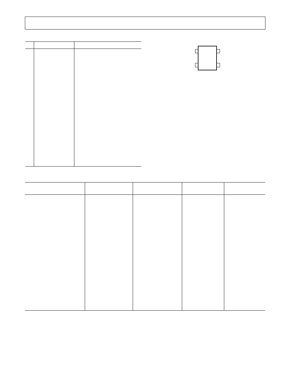
PIN CONFIGURATION
1
2
TOP VIEW
(Not to Scale)
4
3
GND
ADM811/
ADM812
RESET
/RESET
V
CC
MR
ORDERING GUIDE
Reset
Temperature
Brand
Model*
Threshold
Range
Information
Quantity
ADM811LART-REEL
4.63 V
40
°
C to +85
°
C
MBV
10K
ADM811LART-REEL-7
4.63 V
40
°
C to +85
°
C
MBV
3K
ADM811MART-REEL
4.38 V
40
°
C to +85
°
C
MBT
10K
ADM811MART-REEL-7
4.38 V
40
°
C to +85
°
C
MBT
3K
ADM811TART-REEL
3.08 V
40
°
C to +85
°
C
MBG
10K
ADM811TART-REEL-7
3.08 V
40
°
C to +85
°
C
MBG
3K
ADM811-3TART-REEL
3.08 V
40
°
C to +85
°
C
MB3
10K
ADM811-3TART-RL7
3.08 V
40
°
C to +85
°
C
MB3
3K
ADM811SART-REEL
2.93 V
40
°
C to +85
°
C
MBE
10K
ADM811SART-REEL-7
2.93 V
40
°
C to +85
°
C
MBE
3K
ADM811RART-REEL
2.63 V
40
°
C to +85
°
C
MBB
10K
ADM811RART-REEL-7
2.63 V
40
°
C to +85
°
C
MBB
3K
ADM812LART-REEL
4.63 V
40
°
C to +85
°
C
MCV
10K
ADM812LART-REEL-7
4.63 V
40
°
C to +85
°
C
MCV
3K
ADM812MART-REEL
4.38 V
40
°
C to +85
°
C
MCT
10K
ADM812MART-REEL-7
4.38 V
40
°
C to +85
°
C
MCT
3K
ADM812TART-REEL
3.08 V
40
°
C to +85
°
C
MCG
10K
ADM812TART-REEL-7
3.08 V
40
°
C to +85
°
C
MCG
3K
ADM812SART-REEL
2.93 V
40
°
C to +85
°
C
MCE
10K
ADM812SART-REEL-7
2.93 V
40
°
C to +85
°
C
MCE
3K
ADM812RART-REEL
2.63 V
40
°
C to +85
°
C
MCB
10K
ADM812RART-REEL-7
2.63 V
40
°
C to +85
°
C
MCB
3K
*Only available in reels.
Parts in bold are ex-stock, please contact factory for availability.
ADM811/ADM812
4
REV. 0
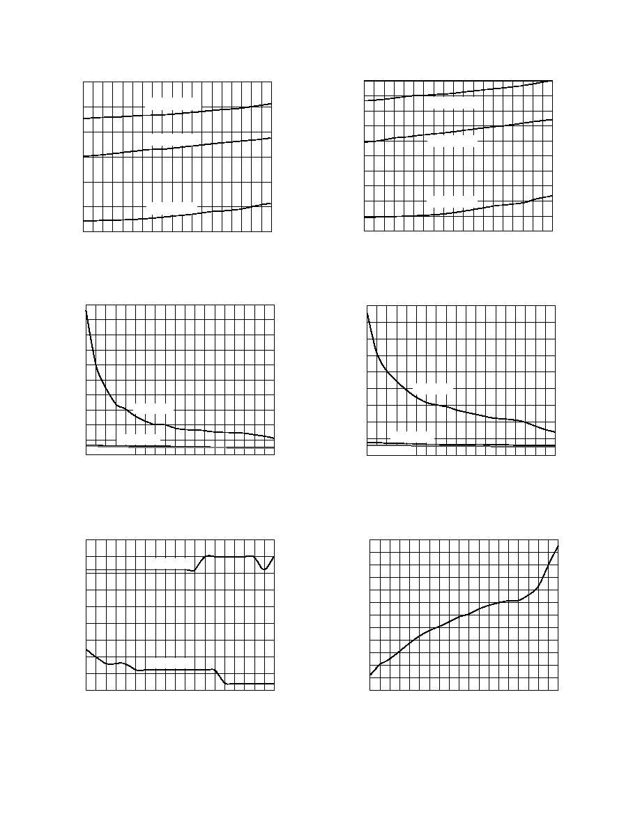
Typical Performance Characteristics
TEMPERATURE C
12
40
10
8
6
4
2
0
30
20
10
0
10
20
25
30
40
50
60
70
80
85
90
100
110
120
125
I
DD
A
I
DD
@ V
CC
= 5.5V
I
DD
@ V
CC
= 3V
I
DD
@ V
CC
= 1V
Figure 2. Supply Current vs. Temperature (ADM81_R/S/T)
TEMPERATURE C
1000
40
POWER-DOWN RESET DELAY
s
30
20
10
0
10
20
25
30
40
50
60
70
80
85
90
100
110
120
125
V
OD
= 20mV
V
OD
= 200mV
V
OD
= 125mV
900
800
700
600
500
400
300
200
100
0
Figure 3. Power-Down RESET Delay vs. Temperature
(ADM81__R/S/T)
TEMPERATURE C
289
40
POWER-UP RESET TIMEOUT ms
30
20
10
0
10
20
25
30
40
50
60
70
80
85
90
100
110
120
125
284
279
274
269
264
259
254
249
244
ADM81_L/M
ADM81_R/S/T
Figure 4. Power-Up Reset Timeout vs. Temperature
TEMPERATURE C
10
40
I
DD
A
30
20
10
0
10
20
25
30
40
50
60
70
80
85
90
100
110
120
125
9
8
7
6
5
4
3
2
1
0
I
DD
@ V
CC
= 5.5V
I
DD
@ V
CC
= 3V
I
DD
@ V
CC
= 1V
Figure 5. Supply Current vs. Temperature (ADM81_L/M)
TEMPERATURE C
900
40
POWER-DOWN RESET DELAY
s
30
20
10
0
10
20
25
30
40
50
60
70
80
85
90
100
110
120
125
800
700
600
500
400
300
200
100
0
V
OD
= 20mV
V
OD
= 200mV
V
OD
= 125mV
Figure 6. Power-Down RESET Delay vs. Temperature
(ADM81_L/M)
TEMPERATURE C
1.007
40
NORMALIZED RESET THRESHOLD
30
20
10
0
10
20
25
30
40
50
60
70
80
85
90
100
110
120
125
1.006
1.005
1.004
1.003
1.002
1.001
1.000
0.999
0.998
0.997
0.996
0.995
Figure 7. Reset Threshold Deviation vs. Temperature
ADM811/ADM812
5
REV. 0
CIRCUIT INFORMATION
RESET THRESHOLDS
The reset output provides a
RESET (for the ADM811) or a
RESET (for the ADM812) output to the microprocessor when-
ever the V
CC
input is below the reset threshold. The actual reset
threshold is dependant on whether a L, M, T, S or R suffix is
used. Please refer to Table I.
Table I. Reset Threshold Options
RESET
Model
Threshold
ADM811LART
4.63 V
ADM811MART
4.38 V
ADM811TART
3.08 V
ADM811-3TART
3.08 V
ADM811SART
2.93 V
ADM811RART
2.63 V
ADM812LART
4.63 V
ADM812MART
4.38 V
ADM812TART
3.08 V
ADM812SART
2.93 V
ADM812RART
2.63 V
Parts in bold type are ex-stock, please contact factory for availability.
RESET OUTPUT
On power-up and after V
CC
rises above the reset threshold, an
internal timer holds the reset output active for 240 ms (typical).
This is intended as a power-on reset signal for the processor. It
allows time for both the power supply and the microprocessor
to stabilize after power-up. If a power supply brownout or inter-
ruption occurs, the reset output is similarly activated and re-
mains active for 240 ms (typical) after the supply recovers. This
allows time for the power supply and microprocessor to stabilize.
The ADM811 provides an active low reset output (
RESET)
while the ADM812 provides an active high output (RESET).
During power-down of the ADM811, the
RESET output re-
mains valid (low) with V
CC
as low as 1 V. This ensures that the
microprocessor is held in a stable shutdown condition as the
supply falls and also ensures that no spurious activity can occur
via the
µ
P as it powers up.
MANUAL RESET
The ADM811/ADM812 is equipped with a manual reset input.
This input is designed to operate in a noisy environment where
unwanted glitches could be induced. These glitches could be
produced by the bouncing action of a switch contact or where a
Manual Reset switch may be located some distance away from
the circuit (the cabling of which may pickup noise).
The Manual Reset input is guaranteed to ignore logically valid
inputs which are faster than 100 ns and accept inputs longer in
duration than 10
µ
s.
GLITCH IMMUNITY
The ADM811/ADM812 contain internal filtering circuitry
providing glitch immunity from fast transient glitches on the
power supply line.
RESET
V
REF
V
REF
V
REF
V
REF
t
1
t
1
V
CC
t
1
=
RESET
TIME = 240ms TYPICAL
V
REF
=
RESET
VOLTAGE THRESHOLD
Figure 8. Power Fail
RESET Timing
INTERFACING TO OTHER DEVICES
Output
The ADM811/ADM812 series is designed to integrate with
as many devices as possible. One feature of the ADM811/
ADM812 is the reset output, which is directly proportional to
V
CC
(this is guaranteed only while V
CC
is greater than 1 V). This
enables the part to be used in both 3 V and 5 V or any nominal
voltage within the minimum and maximum specifications for V
CC
.
THE BENEFITS OF A VERY ACCURATE RESET
THRESHOLD
Because the ADM811/ADM812 series can operate effectively
even when there are large degradations of the supply voltages,
the possibility of a malfunction during a power failure is greatly
reduced. Another advantage of the ADM811/ADM812 series is
its very accurate internal voltage reference circuit. Combined,
these benefits produce an exceptionally reliable Microprocessor
Supervisory Circuit.
RESET
ADM811
GND
V
CC
V
CC
Figure 9. Ensuring a Valid
RESET Output Down to
V
CC
= 0 V
ENSURING A VALID RESET OUTPUT DOWN TO
V
CC
= 0 V
When V
CC
falls below 0.8 V, ADM811s
RESET no longer sinks
current. Therefore, a high impedance CMOS logic input con-
nected to RESET may drift to undetermined logic levels. To
eliminate this problem a 100 k
resistor should be connected
from
RESET to ground.
ADM811/ADM812
6
REV. 0
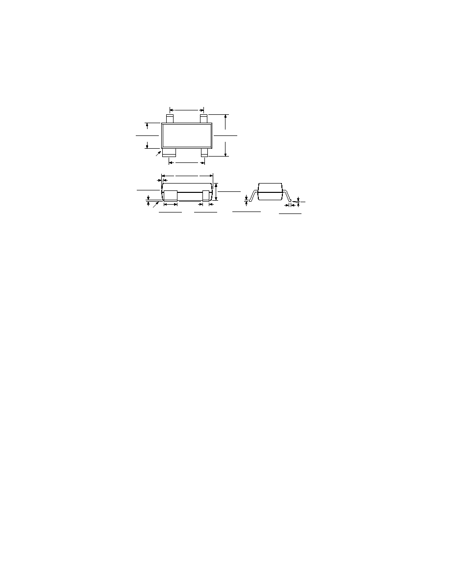
OUTLINE DIMENSIONS
Dimensions shown in inches and (mm).
C314083/99
PRINTED IN U.S.A.
4-Lead Plastic Surface Mount Package
(SOT-143)
0.037 (0.94)
0.030 (0.77)
SEATING
PLANE
0.021 (0.54)
0.015 (0.38)
0.004 (0.10)
0.001 (0.03)
7
0.120 (3.05)
0.105 (2.67)
0.040 (1.02)
0.031 (0.79)
PIN 1
0.079 (2.00)
0.071 (1.80)
1
2
3
4
0.055 (1.40)
0.047 (1.20)
0.098 (2.50)
0.083 (2.10)
0.080 (2.03)
0.070 (1.78)
8
0
0.010 (0.25)
0.005 (0.13)
0.0059 (0.089)
0.0035 (0.15)